US4528480A - AC Drive type electroluminescent display device - Google Patents
AC Drive type electroluminescent display deviceDownload PDFInfo
- Publication number
- US4528480A US4528480AUS06/454,008US45400882AUS4528480AUS 4528480 AUS4528480 AUS 4528480AUS 45400882 AUS45400882 AUS 45400882AUS 4528480 AUS4528480 AUS 4528480A
- Authority
- US
- United States
- Prior art keywords
- transistor
- gate
- electrode
- display device
- electroluminescent
- Prior art date
- Legal status (The legal status is an assumption and is not a legal conclusion. Google has not performed a legal analysis and makes no representation as to the accuracy of the status listed.)
- Expired - Lifetime
Links
Images


Classifications
- H—ELECTRICITY
- H10—SEMICONDUCTOR DEVICES; ELECTRIC SOLID-STATE DEVICES NOT OTHERWISE PROVIDED FOR
- H10D—INORGANIC ELECTRIC SEMICONDUCTOR DEVICES
- H10D30/00—Field-effect transistors [FET]
- H10D30/60—Insulated-gate field-effect transistors [IGFET]
- H10D30/67—Thin-film transistors [TFT]
- H10D30/6704—Thin-film transistors [TFT] having supplementary regions or layers in the thin films or in the insulated bulk substrates for controlling properties of the device
- H10D30/6713—Thin-film transistors [TFT] having supplementary regions or layers in the thin films or in the insulated bulk substrates for controlling properties of the device characterised by the properties of the source or drain regions, e.g. compositions or sectional shapes
- H10D30/6715—Thin-film transistors [TFT] having supplementary regions or layers in the thin films or in the insulated bulk substrates for controlling properties of the device characterised by the properties of the source or drain regions, e.g. compositions or sectional shapes characterised by the doping profiles, e.g. having lightly-doped source or drain extensions
- G—PHYSICS
- G09—EDUCATION; CRYPTOGRAPHY; DISPLAY; ADVERTISING; SEALS
- G09G—ARRANGEMENTS OR CIRCUITS FOR CONTROL OF INDICATING DEVICES USING STATIC MEANS TO PRESENT VARIABLE INFORMATION
- G09G3/00—Control arrangements or circuits, of interest only in connection with visual indicators other than cathode-ray tubes
- G09G3/20—Control arrangements or circuits, of interest only in connection with visual indicators other than cathode-ray tubes for presentation of an assembly of a number of characters, e.g. a page, by composing the assembly by combination of individual elements arranged in a matrix no fixed position being assigned to or needed to be assigned to the individual characters or partial characters
- G09G3/22—Control arrangements or circuits, of interest only in connection with visual indicators other than cathode-ray tubes for presentation of an assembly of a number of characters, e.g. a page, by composing the assembly by combination of individual elements arranged in a matrix no fixed position being assigned to or needed to be assigned to the individual characters or partial characters using controlled light sources
- G09G3/30—Control arrangements or circuits, of interest only in connection with visual indicators other than cathode-ray tubes for presentation of an assembly of a number of characters, e.g. a page, by composing the assembly by combination of individual elements arranged in a matrix no fixed position being assigned to or needed to be assigned to the individual characters or partial characters using controlled light sources using electroluminescent panels
- H—ELECTRICITY
- H10—SEMICONDUCTOR DEVICES; ELECTRIC SOLID-STATE DEVICES NOT OTHERWISE PROVIDED FOR
- H10D—INORGANIC ELECTRIC SEMICONDUCTOR DEVICES
- H10D30/00—Field-effect transistors [FET]
- H10D30/60—Insulated-gate field-effect transistors [IGFET]
- H10D30/67—Thin-film transistors [TFT]
- H10D30/6729—Thin-film transistors [TFT] characterised by the electrodes
- H10D30/673—Thin-film transistors [TFT] characterised by the electrodes characterised by the shapes, relative sizes or dispositions of the gate electrodes
- H10D30/6731—Top-gate only TFTs
- H—ELECTRICITY
- H10—SEMICONDUCTOR DEVICES; ELECTRIC SOLID-STATE DEVICES NOT OTHERWISE PROVIDED FOR
- H10D—INORGANIC ELECTRIC SEMICONDUCTOR DEVICES
- H10D30/00—Field-effect transistors [FET]
- H10D30/60—Insulated-gate field-effect transistors [IGFET]
- H10D30/67—Thin-film transistors [TFT]
- H10D30/674—Thin-film transistors [TFT] characterised by the active materials
- H10D30/6741—Group IV materials, e.g. germanium or silicon carbide
- H10D30/6743—Silicon
- H10D30/6745—Polycrystalline or microcrystalline silicon
- G—PHYSICS
- G09—EDUCATION; CRYPTOGRAPHY; DISPLAY; ADVERTISING; SEALS
- G09G—ARRANGEMENTS OR CIRCUITS FOR CONTROL OF INDICATING DEVICES USING STATIC MEANS TO PRESENT VARIABLE INFORMATION
- G09G2300/00—Aspects of the constitution of display devices
- G09G2300/08—Active matrix structure, i.e. with use of active elements, inclusive of non-linear two terminal elements, in the pixels together with light emitting or modulating elements
- G09G2300/0809—Several active elements per pixel in active matrix panels
- G09G2300/0842—Several active elements per pixel in active matrix panels forming a memory circuit, e.g. a dynamic memory with one capacitor
- H—ELECTRICITY
- H10—SEMICONDUCTOR DEVICES; ELECTRIC SOLID-STATE DEVICES NOT OTHERWISE PROVIDED FOR
- H10K—ORGANIC ELECTRIC SOLID-STATE DEVICES
- H10K71/00—Manufacture or treatment specially adapted for the organic devices covered by this subclass
- H10K71/841—Applying alternating current [AC] during manufacturing or treatment
Definitions
- This inventionrelates to an AC drive type electroluminescent display device.
- the electroluminescent display devicecomprises a plurality of electroluminescent elements arranged in a matrix on a transparent substrate and transistors for driving the electroluminescent elements are provided corresponding to respective elements. Transistors corresponding to the electroluminescent elements to be operated are selectively driven to cause the elements to luminesce for displaying desired patterns, digits or letters.
- the transistors for driving the electroluminescent elementsare required to be formed on a transparent substrate such as a glass panel and to have a high breakdown voltage characteristic. For this reason, thin film transistors utilizing as their semiconductor layers such binary compounds as CdSe, CdS, etc. have been generally used. Such transistors are described, for example in T. P. Brody et al paper entitled "A 6 ⁇ 6-in 20-lpi Electroluminscent Display Panel; I.E.E.E. Transactions ON Electron Device, Vol. ED-22, No. 9, September 1975.
- Thin film transistors utilizing such binary compoundshave a high mobility of the carriers, and a high breakdown voltage characteristic so that they are suitable for use in the display device of the type described above, but still accompany various problems as follows.
- the binary compound semiconductors utilized in the thin film transistorslack stability of the characteristic, reliability over a long period, and the uniformity of the characteristics of the substrate. These factors cause a short life of the resulting thin film transistors. To obviate these difficulties, it has been proposed to perform all manufacturing steps in vacuum. Even with such measure, however, the characteristics of the thin film transistors vary with time. Typical examples of such characteristics are shown in FIG. 4. At present, it is considered that the instability of the characteristics of the binary compound semiconductors is caused by their stoichiometric compositions.
- the binary compound semiconductorscan not form insulating films by oxidation reaction.
- a gate insulating filmfor example, is formed by sputtering or vapor-depositing of the oxide film of other elements, for instance SiO 2 or Al 2 O 3 .
- the interfaceis not uniform with the result that numerous trap levels are formed at the interface which trap electric charge, thus decreasing drain current, and degrading the characteristic of the interface between the gate insulating film and the semiconductor layer. This also degrades the reproduceability and uniformness of the element characteristics of the thin film transistors.
- a vacuum evaporation maskis used so that the accuracy of mask aligning is about 100 microns so that the width of a pattern formed through a vacuum evaporation mask is about 30 microns and the minimum width of the pattern becomes more than 30 microns. Therefore, it is impossible to increase the picture element density to a value higher than one line/mm when the transistors are combined with electroluminescent elements to fabricate a display device, thus making it difficult to obtain the display device of high density.
- the principal object of this inventionis to provide at a high reproduceability an improved AC drive type electroluminescent display device having a long life.
- Another object of this inventionis to provide a high density AC drive type electroluminescent display device.
- Still another object of this inventionis to provide an AC drive type electroluminescent display device capable of containing thin film transistors having a high breakdown voltage characteristic.
- a further object of this inventionis to provide a thin film transistor having a uniform characteristic and a high reproduceability which can be combined with an electroluminescent element so as to obtain a stable AC drive type electroluminescent display device.
- Still further object of this inventionis to provide an AC drive type electroluminescent display device capable of simplifying the construction of the thin film transistor and hence the manufacturing steps thereof.
- thin film transistors made of polycrystalline siliconare combined with an electroluminescent element, and the thin film transistors for driving the electroluminescent element are formed with offset regions between the source and gate electrodes and between the gate and drain electrodes, that is formed as a bidirectional offset construction.
- an AC drive type electroluminescent display devicecomprising first and second thin film transistors formed on first and second portions of one surface of a transparent insulating substrate, each of which includes a first conductivity type channel region, said channel region comprising polycrystalline silicon with its crystal grain size increased, first and second impurity diffused regions of said first conductivity type and contiguously disposed on both sides of said channel region, a silicon gate oxide film formed on said channel region, a gate region overlying said silicon gate oxide film and made of polycrystalline silicon of a second conductivity type, a gate electrode, and first and second output electrodes which are formed on said gate electrode and said first and second impurity diffused regions respectively, an electroluminescent element formed on a third portion of said surface of said transparent insulating substrate, a capacitance element formed on a fourth portion of said surface of said transparent insulating substrate, means for connecting one electrode of said electroluminescent element to the first output electrode of said second transistor, means for connecting said second output electrode of said second transistor to a
- FIG. 1is a perspective view showing one display cell of one embodiment of an AC drive type electroluminescent display device according to this invention
- FIG. 2is a sectional view taken along a line II--II in FIG. 1;
- FIG. 2Ais an enlarged sectional view showing the construction of a thin film transistor shown in FIG. 2;
- FIG. 3is a connection diagram of the display device in which a plurality of the display cells shown in FIG. 1 are arranged in a matrix;
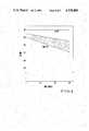
- FIG. 4shows ID/IOD--time characteristics of a CdSe thin film transistor and of a polycrystalline silicon thin film transistor embodying the invention
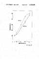
- FIG. 5is a graph showing a breakdown voltage-offset gate length characteristic of a polycrystalline silicon thin film transistor embodying the invention
- FIG. 6is a graph showing the brightness-impressed voltage characteristic of an electroluminescent element
- FIG. 7is a graph showing the breakdown voltage-off set length characteristic at the time of annealing taking laser power variation as a parameter
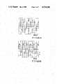
- FIGS. 8A, 8B and 8Care sectional views showing steps of one example of the method of manufacturing a polycrystalline silicon thin film transistor embodying the invention.
- FIG. 9shows the drain current--drain voltage characteristics of the resulting thin film transistor.
- FIGS. 10A and 10Bshow the waveform of the source voltage and the waveforms at the time of ON-OFF operation of an electroluminescent element.
- FIGS. 1, 2 and 3show one embodiment of an AC drive type electroluminescent display device according to this invention, more particularly, a picture element display cell.
- the circuit construction of one picture element display cell utilized in this inventionis shown in FIG. 3.
- each picture element display cellcomprises an electroluminescent cell 11, two thin film transistors 12 and 13 utilizing polycrystalline silicon and a capacitor 14.
- One terminal of the electroluminescent cell 11is connected to a power line 16, while the other terminal is connected to the drain electrode of the thin film transistor 13 of high breakdown voltage type.
- the gate electrode of the transistor 13is connected to the source electrode of the thin film transistor 12, and the source electrode of the thin film transistor 13 is connected to a grounded line 18 acting as a common reference line.
- the drain electrode of the thin film transistor 12is connected to a signal line 20 and the gate electrode is connected to a scanning line 22.
- the source electrode of the transistor 12is connected to the gate electrode of the transistor 13 and to one terminal of the capacitor 14, the other terminal thereof being connected to the grounded line 18.
- the thin film transistor 12When a high level signal is applied to the scanning line 22, the thin film transistor 12 turns ON to charge the capacitor 14 by a current from the signal line 20. When the terminal voltage of the capacitor 14 becomes substantially equal to the voltage of the signal line 20, transistor 13 also turns ON. As a consequence, a drive circuit of the electroluminescent element 11 is formed between the power line 16 and the grounded line 18, whereby an AC voltage of ⁇ 70 V rms, for example, is impressed upon the electroluminescent element 11 from the power line 16 to cause the element 11 to emit. When the transistor 12 is turned OFF as a result of decreasing the voltage of the scanning line 22 below a predetermined value, the charge in the capacitor 14 maintains the transistor 13 in an ON state. During the ON state of the transistor 13 the electroluminescent element 11 continues to emit. When the high level signal is again applied to the scanning line 22 and a low level signal is applied to the signal line 20, the capacitor 14 is dischanged to disenergize the electroluminescent element 11.
- FIGS. 1, 2 and 3Although this circuit construction per se is described in the reference referred to hereinabove, the invention is characterized by a novel combination of such circuit and the electroluminescent element as shown in FIGS. 1, 2 and 3.
- FIG. 1insulating films and protective films not important to understand the invention are omitted, and some of the elements directly related to this invention are partially shown so that the constructions shown in FIGS. 1 and 2 differ slightly.
- spaced N type amorphous silicon or polycrystaline silicon layers 32A and 32Bare formed on one surface of a transparent substrate 31. These silicon layers comprise channel regions 32Aa and 32Ba having a suitable resistivity and regions 32Ab and 32Bb diffused with an N type impurity at a high concentration and positioned on both sides of the channel regions 32Aa and 32Ba.
- Gate oxide films 33A and 33B made of SiO 2are formed on the channel regions 32Aa and 32Ba of the silicon layers, and at the central portions of the gate oxide films 33A and 33B are disposed gate regions 34A and 34B formed by diffusing a P type impurity in the polycrystalline silicon.
- Insulating films 35A and 35B made of SiO 2are formed on the gate regions 34A and 34B, and gate oxide films 33A and 33B.
- the insulating films 35A and 35Bare perforated to receive electrodes 36A and 36B reaching the gate regions 34A and 34B.
- Source and drain electrodes 38A, 38B, 39A and 39Bare disposed on the impurity diffused regions 32Ab and 32Bb in ohmic contact therewith. These source and drain electrodes are made of aluminum layers, for example.
- the channel region 32Aa, impurity diffused region 32Ab, gate oxide film 33A, gate region 34A, gate electrode 36A, drain electrode 38A and source electrode 38Bconstitute the thin film transistor 12 shown in FIG.
- FIG. 2AAn enlarged sectional structure of the transistor 13 is shown in FIG. 2A. Accordingly, the gate electrode 36A of transistor 12 is connected to the scanning line 22 and the drain electrode 38A is connected to the signal line 20, while the gate electrode 36B of transistor 13 is connected to the source electrode 38B of transistor 12 shown in FIG. 3.
- a transparent electrode 41 connected to the drain electrode 39B of the transistor 13is formed on the other portion of the upper surface of the glass substrate 31 and a vacuum evaporated electroluminescent film 43 consisting of an electroluminescent member essentially made of ZnS and doped with Mn acting as luminescent centers is formed on the transparent electrode 41.
- a source electrode 46is disposed on the electroluminescent film 43 via an insulating film 45.
- the transparent electrode 41, vacuum evaporated film 43, insulating film 45, and the source electrode 46constitute the electroluminescent element 11, and the source electrode 46 is connected to the power line 16.
- the insulating film 45As the insulating film 45, higher dielectric materials such as Sm 2 O 3 and Ta 2 O 5 etc. may be used. Mn used as the material for emitting the electroluminescent element 11 may be replaced by TbF 3 , SmF 3 , ErF 3 , or other materials which are used for AC-driving the electroluminescent element. Further, between the transparent electrode 41 and electroluminescent film 43, an additional insulating film may be inserted to constitute the electroluminescent element 11. Also the electroluminescent element 11 may take other structures suitable for AC-driving the element 11.
- An electrode 51 of a capacitor 14consisting of polycrystalline silicon doped with a P type impurity which is the same as that used to form the gate regions of the thin film gate regions 34A and 34B of the thin film transistor is formed on the other portion of the upper surface of the glass substrate 31.
- An SiO 2 insulating film 52is disposed on the electrode 51, and the other electrode 53 of the capacitor 14 is disposed on the insulating film 52.
- the electrode 51is connected to the grounded line 18, while the electrode 53 is connected to the source electrode 38B of transistor 12 and to the gate electrode 36B of the transistor 13.
- offset gate regions 61 and 62are provided between the source and gate regions and between the gate and drain regions of the thin film transistor 13 as clearly shown in FIG. 2A.
- these offset gate regionsare symmetrically disposed on the opposite sides of each gate region in contiguous relation thereto and each gate region has a length of 5 microns, for example.
- the offset gate regions of the transistor 12may be omitted since no high voltage is applied to the transistor 12.
- FIG. 4shows variation with time between the initial drain current IOD and the normal drain current ID.
- the drain current IDdecreases with time as shown by a shaded portion, whereas in the thin film transistor of this invention utilizing polycrystalline silicon the drain current ID does not change in any appreciable extent in the measured period meaning a stable characteristic over a long period.
- the polycrystalline siliconis an assembly of crystal grains there are many interfaces between the grains which are effective to increase the breakdown voltage of the thin film transistor as well as the mutual conductance.
- the electroluminescent element now being useddoes not illuminate or radiate unless an effective voltage of higher than about 40 V is applied.
- an effective voltage of higher than about 40 Vis applied.
- a voltage of about 70 Vrmsis used. Accordingly, a practical device can be obtained by increasing the insulating strength to a value higher than 100 V by increasing the offset length to be longer than 5 microns by taking a sufficient safty margin into consideration. If it is desired to have higher breakdown voltage, the offset gate length is increased.
- the electroluminescent element materialis improved thus permitting use of the thin film transistors having lower breakdown voltage, the offset gate length can be decreased.
- the channel regionis made of monocrystalline silicon
- the following discussionwill be made.
- monocrystalline siliconis used for the purpose of obtaining a breakdown voltage higher than 100 V it is essential to increase the offset gate length to more than 15 microns. This means that it is necessary to increase the length of the offset gate length than a case utilizing polycrystalline silicon to obtain the same breakdown voltage.
- the thin film transistor utilizing polycrystalline siliconcan be miniaturized than that utilizing monocrystalline silicon.
- the interface characteristicis improved further which also contributes to the desired result of obtaining a stable electroluminescent display device.
- the polycrystalline siliconcomprises an assembly of elongated crystals extending in the direction of x (a direction interconnecting the source and drain electrodes), for example.
- the mobility of carriers in the crystal grainsis substantially the same as that in monocrystalline silicon.
- the crystal grainsare long in the direction of x, although the mobility decreases more or less at the grain interfaces, it is possible to obtain a carrier mobility close to that of monocrystalline silicon.
- FIG. 7shows the relationship between the offset gate length and the element insulating strength when the laser power Po is varied at the time of laser annealing.
- the breakdown voltage with respect to the offset gate lengthslightly increases, but near a range in which the offset gate length is 5 microns as described above the breakdown voltage is substantially constant irrespective of the magnitude of the laser power. This shows that near the offset gate length of about 5 microns now being used, slight variation in the laser power does not cause any variation in the breakdown voltage thereby providing a thin film transistor having uniform characteristics.
- the thin film transistors for driving the electroluminescent elementsare made of polycrystalline silicon it is possible to use a method of preparing conventional elements utilizing a monocrystalline silicon substrate.
- the channel length of the thin film transistorsmay be about 3 to 5 microns, and the width of the elements may be about 20 microns.
- the size of the capacitorcan be reduced even with the conventional method, whereby the picture element density can be increased to 4 lines/mm, which is four times the density of the prior art.
- a silicon film 102 having a thickness of 0.5 micronis deposited on a glass substrate 100 with reduced pressure CVD method using SiH 4 Pyrolysis at a temperature 580° C. for about 37 minutes as shown in FIG. 8A.
- ions of phosphor, an N type impurityare implanted into the film 102 at an implantation voltage of 150 KV to a concentration of 3 ⁇ 10 12 /cm 2 .
- the assemblyis annealed for 30 minutes at a temperature of 900° C.
- the film 102is annealed by using the second harmonic of a laser beam having a diameter of 85 microns, a wavelength of 0.53 micron and a power of 1.6 Joules/cm 2 generated by a YAG laser.
- the irradiation of the laser beamis firstly made in the direction x (horizontal direction in FIG. 8A) at a scanning speed of 100 mm/sec.
- the crystals of the polycrystalline silicongrow in the direction of x at the first irradiation in the x direction but the crystals are not caused to grow by the irradiation in the direction of y.
- the crystal grains grown in the direction xhave a length of about 10 microns, while the width of the grains grown in the direction y is only one micron.
- the laser beam annealingis effected for the purpose of growing crystal grains and electrically activating them.
- the laser beam irradiation of the film 102is not limited to the portion to become a channel region but portions on both sides of the channel region are also irradiated.
- the assemblyis heated in dry oxygen for 90 minutes at a temperature of 1100° C. for forming an SiO 2 gate oxide film 105 having a thickness of 1500 angstroms on the film 102. Then the film 102 and the gate oxide film 105 are worked to have predetermined patterns by photolithography and plasma etching in CF 4 gas.
- a layer of polycrystalline silicon having a thickness of 0.3 micronis formed on the gate oxide film and then the ions of boron acting as a P type impurity are implanted under an implantation voltage of 30 KV to create a concentration of 3 ⁇ 10 15 /cm 2 . Thereafter the assembly is annealed for 15 minutes to form a gate region 106. Then a SiO 2 insulating film 107 is deposited on the gate region 106 by CVD method and portions to form source and drain regions are removed by photolithography and etching techniques.
- ions of arsenic acting as an N type impurityare implanted into the film 102 under an implantation voltage of 100 KV to obtain a high concentration of 2 ⁇ 10 16 /cm 3 and annealed for 30 minutes at 900° C. to form impurity diffused layers 102b utilized as source and drain regions.
- a portion between the impurity diffused layers 102b of the film 102forms a channel region 102a.
- a windowis formed through the insulating film 107 at a portion corresponding to the gate region 106 by photolithography and etching techniques. Then an aluminum layer is deposited with an electron beam to a thickness of 8000 angstroms. Then the aluminum layer is worked accordingly to a predetermined pattern to form electrodes 108, 109 and 110.
- FIG. 9shows a drain current-drain voltage characteristic of a thin film transistor taking the gate voltage as a parameter.
- the offset gate length of the transistoris 5 microns
- the channel lengthis 10 microns
- the channel widthis 100 microns
- the laser anneal poweris 1.6 J/cm 2 .
- the breakdown voltage of the transistoris higher than 100 V
- its mutual conductanceis 25 ⁇ S
- the threshold voltageis 8 V. It should be noted that where the source-channel-drain region of the thinfilm transistor 13 is an N 30 -N-N + structure, the breakdown voltage of the thin film transistor is higher than that of the thin film transistor having an N + -P-N + structure. This is the reason why, where the polycrystalline silicon is used, the breakdown voltage of the P-N junction becomes lower.
- an electroluminescent display deviceincluding a display cell as shown in FIG. 3 by combining the aforementioned thin film transistor and an electroluminescent element
- a source voltage having a waveform as shown in FIG. 10Ais impressed upon the source line 16.
- the terminal voltage waveform of the electroluminescent elementbecomes as shown in FIG. 10B, in which a waveform C shows the waveform of the electroluminescent element when its drive transistor is OFF, while D shows the waveform when the transistor is ON.
- a novel electroluminescent display apparatusin which electroluminescent elements can be positively driven.
- the conductivity type of the gate regions of a transistor for driving an electroluminescent element and a switching transistor for the first mentioned transistormay be of P type.
Landscapes
- Engineering & Computer Science (AREA)
- Physics & Mathematics (AREA)
- Computer Hardware Design (AREA)
- General Physics & Mathematics (AREA)
- Theoretical Computer Science (AREA)
- Electroluminescent Light Sources (AREA)
- Thin Film Transistor (AREA)
- Devices For Indicating Variable Information By Combining Individual Elements (AREA)
Abstract
Description
Claims (8)
Applications Claiming Priority (4)
| Application Number | Priority Date | Filing Date | Title |
|---|---|---|---|
| JP56215038AJPS58115864A (en) | 1981-12-28 | 1981-12-28 | semiconductor equipment |
| JP56-215038 | 1981-12-28 | ||
| JP57209123AJPS5999480A (en) | 1982-11-29 | 1982-11-29 | Display |
| JP57-209123 | 1982-11-29 |
Publications (1)
| Publication Number | Publication Date |
|---|---|
| US4528480Atrue US4528480A (en) | 1985-07-09 |
Family
ID=26517237
Family Applications (1)
| Application Number | Title | Priority Date | Filing Date |
|---|---|---|---|
| US06/454,008Expired - LifetimeUS4528480A (en) | 1981-12-28 | 1982-12-28 | AC Drive type electroluminescent display device |
Country Status (1)
| Country | Link |
|---|---|
| US (1) | US4528480A (en) |
Cited By (52)
| Publication number | Priority date | Publication date | Assignee | Title |
|---|---|---|---|---|
| DE4112078A1 (en)* | 1990-04-12 | 1991-10-17 | Futaba Denshi Kogyo Kk | DISPLAY DEVICE |
| US5177406A (en)* | 1991-04-29 | 1993-01-05 | General Motors Corporation | Active matrix vacuum fluorescent display with compensation for variable phosphor efficiency |
| US5194290A (en)* | 1987-12-31 | 1993-03-16 | The United States Of America As Represented By The Administrator Of The National Aeronautics And Space Administration | Method of making a single layer multi-color luminescent display |
| WO1993024921A1 (en)* | 1992-06-02 | 1993-12-09 | David Sarnoff Research Center, Inc. | Active matrix electroluminescent display and method of operation |
| US5302468A (en)* | 1992-01-28 | 1994-04-12 | Pioneer Electronic Corporation | Organic electroluminescent display apparatus |
| US5386179A (en)* | 1990-06-20 | 1995-01-31 | Fuji Xerox Co., Ltd. | AC power driven electroluminescent device |
| US5463279A (en)* | 1994-08-19 | 1995-10-31 | Planar Systems, Inc. | Active matrix electroluminescent cell design |
| US5495119A (en)* | 1992-07-23 | 1996-02-27 | Nec Corporation | MOS thin film transistor having high breakdown voltage |
| WO1996006456A1 (en)* | 1994-08-24 | 1996-02-29 | David Sarnoff Research Center, Inc. | Active matrix electroluminescent display pixel and method of fabricating same |
| US5548132A (en)* | 1994-10-24 | 1996-08-20 | Micron Technology, Inc. | Thin film transistor with large grain size DRW offset region and small grain size source and drain and channel regions |
| DE19624841A1 (en)* | 1995-06-23 | 1997-01-02 | Planar Systems Inc | Substrate carrier for electroluminescent displays |
| US5644327A (en)* | 1995-06-07 | 1997-07-01 | David Sarnoff Research Center, Inc. | Tessellated electroluminescent display having a multilayer ceramic substrate |
| US5698864A (en)* | 1982-04-13 | 1997-12-16 | Seiko Epson Corporation | Method of manufacturing a liquid crystal device having field effect transistors |
| EP0717439A3 (en)* | 1994-12-14 | 1999-06-02 | Eastman Kodak Company | A method of fabricating a TFT-EL pixel |
| EP0923134A1 (en)* | 1993-02-10 | 1999-06-16 | Seiko Epson Corporation | Active matrix circuit board and method of manufacturing it |
| US6013928A (en)* | 1991-08-23 | 2000-01-11 | Semiconductor Energy Laboratory Co., Ltd. | Semiconductor device having interlayer insulating film and method for forming the same |
| US6091203A (en)* | 1998-03-31 | 2000-07-18 | Nec Corporation | Image display device with element driving device for matrix drive of multiple active elements |
| US6104041A (en)* | 1994-08-24 | 2000-08-15 | Sarnoff Corporation | Switching circuitry layout for an active matrix electroluminescent display pixel with each pixel provided with the transistors |
| US6147375A (en)* | 1992-02-05 | 2000-11-14 | Semiconductor Energy Laboratory Co., Ltd. | Active matrix display device |
| US6221701B1 (en)* | 1984-05-18 | 2001-04-24 | Semiconductor Energy Laboratory Co., Ltd. | Insulated gate field effect transistor and its manufacturing method |
| US6229506B1 (en) | 1997-04-23 | 2001-05-08 | Sarnoff Corporation | Active matrix light emitting diode pixel structure and concomitant method |
| EP0901163A3 (en)* | 1997-09-08 | 2001-05-16 | Sanyo Electric Co., Limited. | Semiconductor device having laser-annealed semiconductor elements, and display device using this semiconductor device |
| US6246180B1 (en)* | 1999-01-29 | 2001-06-12 | Nec Corporation | Organic el display device having an improved image quality |
| WO2001073737A1 (en)* | 2000-03-30 | 2001-10-04 | Seiko Epson Corporation | Display |
| GB2367414A (en)* | 2000-09-28 | 2002-04-03 | Seiko Epson Corp | Display device using TFT's |
| US6456013B1 (en) | 1999-09-30 | 2002-09-24 | Sanyo Electric Co., Ltd. | Thin film transistor and display device |
| US6498592B1 (en) | 1999-02-16 | 2002-12-24 | Sarnoff Corp. | Display tile structure using organic light emitting materials |
| US20030058212A1 (en)* | 1991-10-16 | 2003-03-27 | Yasunhiko Takemura | Process of operating active matrix display device having thin film transistors |
| US20030111964A1 (en)* | 2001-12-18 | 2003-06-19 | Koninklijke Philips Electronics N.V. | Electroluminescent display device |
| US6653996B2 (en)* | 2000-03-28 | 2003-11-25 | Sanyo Electric Co., Ltd. | Display device |
| US6693301B2 (en) | 1991-10-16 | 2004-02-17 | Semiconductor Energy Laboratory Co., Ltd. | Electro-optical device and method of driving and manufacturing the same |
| KR100430929B1 (en)* | 2000-03-30 | 2004-05-12 | 세이코 엡슨 가부시키가이샤 | Display |
| US20040185641A1 (en)* | 2000-11-20 | 2004-09-23 | Hiroshi Tanabe | Thin film transistor having high mobility and high on-current and method for manufacturing the same |
| US20040207777A1 (en)* | 1991-02-16 | 2004-10-21 | Semiconductor Energy Laboratory Co., Ltd. | Electro-optical device |
| US20050017932A1 (en)* | 1999-02-25 | 2005-01-27 | Canon Kabushiki Kaisha | Image display apparatus and method of driving image display apparatus |
| US20050067971A1 (en)* | 2003-09-29 | 2005-03-31 | Michael Gillis Kane | Pixel circuit for an active matrix organic light-emitting diode display |
| US20050078104A1 (en)* | 1998-02-17 | 2005-04-14 | Matthies Dennis Lee | Tiled electronic display structure |
| US20050104514A1 (en)* | 2000-12-14 | 2005-05-19 | Kim Hye-Dong | Organic EL device and method for manufacturing the same |
| US20050112813A1 (en)* | 2003-11-24 | 2005-05-26 | Keum-Nam Kim | Method for manufacturing transistor and image display device using the same |
| US20050146262A1 (en)* | 1995-03-24 | 2005-07-07 | Semiconductor Energy Laboratory Co., Ltd. | Thin film transistor, organic electroluminescence display device and manufacturing method of the same |
| US6980272B1 (en) | 2000-11-21 | 2005-12-27 | Sarnoff Corporation | Electrode structure which supports self alignment of liquid deposition of materials |
| US7071910B1 (en) | 1991-10-16 | 2006-07-04 | Semiconductor Energy Laboratory Co., Ltd. | Electrooptical device and method of driving and manufacturing the same |
| US20070097060A1 (en)* | 2005-10-31 | 2007-05-03 | Nec Electronics Corporation | Liquid crystal display driver, and liquid crystal display apparatus using the same |
| US7253440B1 (en)* | 1991-10-16 | 2007-08-07 | Semiconductor Energy Laboratory Co., Ltd. | Semiconductor device having at least first and second thin film transistors |
| US7569408B1 (en) | 1991-03-06 | 2009-08-04 | Semiconductor Energy Laboratory Co., Ltd. | Semiconductor device and method for forming the same |
| US7633470B2 (en) | 2003-09-29 | 2009-12-15 | Michael Gillis Kane | Driver circuit, as for an OLED display |
| US20120032162A1 (en)* | 2010-08-04 | 2012-02-09 | Semiconductor Energy Laboratory Co., Ltd. | Semiconductor device |
| US20120292612A1 (en)* | 2011-05-20 | 2012-11-22 | Samsung Mobile Display Co., Ltd. | Backplane for flat panel display apparatus, flat panel display apparatus, and method of manufacturing the backplane |
| US8675394B2 (en) | 2010-08-04 | 2014-03-18 | Semiconductor Energy Laboratory Co., Ltd. | Semiconductor memory device with oxide semiconductor transistor |
| US9431431B2 (en) | 1999-02-23 | 2016-08-30 | Semiconductor Energy Laboratory Co., Ltd. | Semiconductor device and fabrication method thereof |
| US9589504B2 (en)* | 2013-07-25 | 2017-03-07 | Boe Technology Group Co., Ltd. | OLED AC driving circuit, driving method and display device |
| US9837451B2 (en) | 1999-04-27 | 2017-12-05 | Semiconductor Energy Laboratory Co., Ltd. | Electronic device and electronic apparatus |
Citations (6)
| Publication number | Priority date | Publication date | Assignee | Title |
|---|---|---|---|---|
| US3909306A (en)* | 1973-02-07 | 1975-09-30 | Hitachi Ltd | MIS type semiconductor device having high operating voltage and manufacturing method |
| US4006383A (en)* | 1975-11-28 | 1977-02-01 | Westinghouse Electric Corporation | Electroluminescent display panel with enlarged active display areas |
| US4042854A (en)* | 1975-11-21 | 1977-08-16 | Westinghouse Electric Corporation | Flat panel display device with integral thin film transistor control system |
| US4087792A (en)* | 1977-03-03 | 1978-05-02 | Westinghouse Electric Corp. | Electro-optic display system |
| US4344080A (en)* | 1978-12-05 | 1982-08-10 | Siemens Aktiengesellschaft | Field effect transistor |
| US4394674A (en)* | 1979-10-09 | 1983-07-19 | Nippon Electric Co., Ltd. | Insulated gate field effect transistor |
- 1982
- 1982-12-28USUS06/454,008patent/US4528480A/ennot_activeExpired - Lifetime
Patent Citations (6)
| Publication number | Priority date | Publication date | Assignee | Title |
|---|---|---|---|---|
| US3909306A (en)* | 1973-02-07 | 1975-09-30 | Hitachi Ltd | MIS type semiconductor device having high operating voltage and manufacturing method |
| US4042854A (en)* | 1975-11-21 | 1977-08-16 | Westinghouse Electric Corporation | Flat panel display device with integral thin film transistor control system |
| US4006383A (en)* | 1975-11-28 | 1977-02-01 | Westinghouse Electric Corporation | Electroluminescent display panel with enlarged active display areas |
| US4087792A (en)* | 1977-03-03 | 1978-05-02 | Westinghouse Electric Corp. | Electro-optic display system |
| US4344080A (en)* | 1978-12-05 | 1982-08-10 | Siemens Aktiengesellschaft | Field effect transistor |
| US4394674A (en)* | 1979-10-09 | 1983-07-19 | Nippon Electric Co., Ltd. | Insulated gate field effect transistor |
Non-Patent Citations (4)
| Title |
|---|
| "A 6×6-in 20-lpi Electroluminescent Display Panel" by T. P. Brody et al., IEEE Transactions on Electron Devices, vol. ED-22, No. 9, Sep. 1975. |
| "Thin-Film-Transistor Switching Matrix for Flat-Panel Displays" by G. Kramer; IEEE Transaction on Electron Devices, vol. ED-22, No. 9, pp. 733-739, Sep. 1975. |
| A 6 6 in 20 lpi Electroluminescent Display Panel by T. P. Brody et al., IEEE Transactions on Electron Devices, vol. ED 22, No. 9, Sep. 1975.* |
| Thin Film Transistor Switching Matrix for Flat Panel Displays by G. Kramer; IEEE Transaction on Electron Devices, vol. ED 22, No. 9, pp. 733 739, Sep. 1975.* |
Cited By (116)
| Publication number | Priority date | Publication date | Assignee | Title |
|---|---|---|---|---|
| US5698864A (en)* | 1982-04-13 | 1997-12-16 | Seiko Epson Corporation | Method of manufacturing a liquid crystal device having field effect transistors |
| US6221701B1 (en)* | 1984-05-18 | 2001-04-24 | Semiconductor Energy Laboratory Co., Ltd. | Insulated gate field effect transistor and its manufacturing method |
| US6635520B1 (en) | 1984-05-18 | 2003-10-21 | Semiconductor Energy Laboratory Co., Ltd. | Operation method of semiconductor devices |
| US6680486B1 (en) | 1984-05-18 | 2004-01-20 | Semiconductor Energy Laboratory Co., Ltd. | Insulated gate field effect transistor and its manufacturing method |
| US6734499B1 (en) | 1984-05-18 | 2004-05-11 | Semiconductor Energy Laboratory Co., Ltd. | Operation method of semiconductor devices |
| US5194290A (en)* | 1987-12-31 | 1993-03-16 | The United States Of America As Represented By The Administrator Of The National Aeronautics And Space Administration | Method of making a single layer multi-color luminescent display |
| US5153483A (en)* | 1990-04-12 | 1992-10-06 | Futaba Denshi Kogyo Kabushiki Kaisha | Display device |
| DE4112078A1 (en)* | 1990-04-12 | 1991-10-17 | Futaba Denshi Kogyo Kk | DISPLAY DEVICE |
| DE4112078C2 (en)* | 1990-04-12 | 1998-07-02 | Futaba Denshi Kogyo Kk | Display device |
| US5386179A (en)* | 1990-06-20 | 1995-01-31 | Fuji Xerox Co., Ltd. | AC power driven electroluminescent device |
| US20040207777A1 (en)* | 1991-02-16 | 2004-10-21 | Semiconductor Energy Laboratory Co., Ltd. | Electro-optical device |
| US20050001965A1 (en)* | 1991-02-16 | 2005-01-06 | Semiconductor Energy Laboratory Co., Ltd. | Electro-optical device |
| US7420628B1 (en) | 1991-02-16 | 2008-09-02 | Semiconductor Energy Laboratory Co., Ltd. | Method of making an active-type LCD with digitally graded display |
| US7671827B2 (en) | 1991-02-16 | 2010-03-02 | Semiconductor Energy Laboratory Co., Ltd. | Electro-optical device |
| US7701523B2 (en) | 1991-02-16 | 2010-04-20 | Semiconductor Energy Laboratory Co., Ltd | Electro-optical device |
| US7948569B2 (en) | 1991-02-16 | 2011-05-24 | Semiconductor Energy Laboratory Co., Ltd. | Active matrix type display device |
| US20090021663A1 (en)* | 1991-02-16 | 2009-01-22 | Semiconductor Energy Laboratory Co., Ltd. | Electro-optical device |
| US7646441B2 (en) | 1991-02-16 | 2010-01-12 | Semiconductor Energy Laboratory Co., Ltd. | Electro-optical display device having thin film transistors including a gate insulating film containing fluorine |
| US20050007329A1 (en)* | 1991-02-16 | 2005-01-13 | Semiconductor Energy Laboratory Co., Ltd. | Electro-optical device |
| US7569408B1 (en) | 1991-03-06 | 2009-08-04 | Semiconductor Energy Laboratory Co., Ltd. | Semiconductor device and method for forming the same |
| US5177406A (en)* | 1991-04-29 | 1993-01-05 | General Motors Corporation | Active matrix vacuum fluorescent display with compensation for variable phosphor efficiency |
| US6977392B2 (en) | 1991-08-23 | 2005-12-20 | Semiconductor Energy Laboratory Co., Ltd. | Semiconductor display device |
| US6013928A (en)* | 1991-08-23 | 2000-01-11 | Semiconductor Energy Laboratory Co., Ltd. | Semiconductor device having interlayer insulating film and method for forming the same |
| US6566711B1 (en) | 1991-08-23 | 2003-05-20 | Semiconductor Energy Laboratory Co., Ltd. | Semiconductor device having interlayer insulating film |
| US7071910B1 (en) | 1991-10-16 | 2006-07-04 | Semiconductor Energy Laboratory Co., Ltd. | Electrooptical device and method of driving and manufacturing the same |
| US6693301B2 (en) | 1991-10-16 | 2004-02-17 | Semiconductor Energy Laboratory Co., Ltd. | Electro-optical device and method of driving and manufacturing the same |
| US6759680B1 (en) | 1991-10-16 | 2004-07-06 | Semiconductor Energy Laboratory Co., Ltd. | Display device having thin film transistors |
| US20030058212A1 (en)* | 1991-10-16 | 2003-03-27 | Yasunhiko Takemura | Process of operating active matrix display device having thin film transistors |
| US7116302B2 (en) | 1991-10-16 | 2006-10-03 | Semiconductor Energy Laboratory Co., Ltd. | Process of operating active matrix display device having thin film transistors |
| US7253440B1 (en)* | 1991-10-16 | 2007-08-07 | Semiconductor Energy Laboratory Co., Ltd. | Semiconductor device having at least first and second thin film transistors |
| US5302468A (en)* | 1992-01-28 | 1994-04-12 | Pioneer Electronic Corporation | Organic electroluminescent display apparatus |
| US6147375A (en)* | 1992-02-05 | 2000-11-14 | Semiconductor Energy Laboratory Co., Ltd. | Active matrix display device |
| US6476447B1 (en) | 1992-02-05 | 2002-11-05 | Semiconductor Energy Laboratory Co., Ltd. | Active matrix display device including a transistor |
| USRE40738E1 (en) | 1992-06-02 | 2009-06-16 | Stewart Roger G | Active matrix electroluminescent display and method of operation |
| US5302966A (en)* | 1992-06-02 | 1994-04-12 | David Sarnoff Research Center, Inc. | Active matrix electroluminescent display and method of operation |
| WO1993024921A1 (en)* | 1992-06-02 | 1993-12-09 | David Sarnoff Research Center, Inc. | Active matrix electroluminescent display and method of operation |
| US5495119A (en)* | 1992-07-23 | 1996-02-27 | Nec Corporation | MOS thin film transistor having high breakdown voltage |
| EP0923134A1 (en)* | 1993-02-10 | 1999-06-16 | Seiko Epson Corporation | Active matrix circuit board and method of manufacturing it |
| KR100309935B1 (en)* | 1993-02-10 | 2002-06-20 | 구사마 사부로 | Active Matrix Substrates, Thin Film Transistors and Their Manufacturing Methods |
| US5463279A (en)* | 1994-08-19 | 1995-10-31 | Planar Systems, Inc. | Active matrix electroluminescent cell design |
| US5932892A (en)* | 1994-08-24 | 1999-08-03 | Sarnoff Corporation | High-voltage transistor |
| KR100385378B1 (en)* | 1994-08-24 | 2003-07-16 | 사르노프 코포레이션 | Active matrix electroluminescent display pixel and method of fabricating same |
| EP0776526A4 (en)* | 1994-08-24 | 1998-04-29 | Sarnoff David Res Center | ELECTROLUMINESCENT DISPLAY PIXELS WITH ACTIVE MATRIX AND MANUFACTURING METHOD THEREFOR |
| US5587329A (en)* | 1994-08-24 | 1996-12-24 | David Sarnoff Research Center, Inc. | Method for fabricating a switching transistor having a capacitive network proximate a drift region |
| WO1996006456A1 (en)* | 1994-08-24 | 1996-02-29 | David Sarnoff Research Center, Inc. | Active matrix electroluminescent display pixel and method of fabricating same |
| US6104041A (en)* | 1994-08-24 | 2000-08-15 | Sarnoff Corporation | Switching circuitry layout for an active matrix electroluminescent display pixel with each pixel provided with the transistors |
| US5936262A (en)* | 1994-10-24 | 1999-08-10 | Micron Technology, Inc. | Thin film transistors |
| US6214652B1 (en) | 1994-10-24 | 2001-04-10 | Micron Technology, Inc. | Thin film transistors and method of forming thin film transistors |
| US5548132A (en)* | 1994-10-24 | 1996-08-20 | Micron Technology, Inc. | Thin film transistor with large grain size DRW offset region and small grain size source and drain and channel regions |
| US6420219B2 (en) | 1994-10-24 | 2002-07-16 | Micron Technology, Inc. | Thin film transistors and method of forming thin film transistors |
| US6017782A (en)* | 1994-10-24 | 2000-01-25 | Micron Technology, Inc. | Thin film transistor and method of forming thin film transistors |
| US5904513A (en)* | 1994-10-24 | 1999-05-18 | Micron Technology, Inc. | Method of forming thin film transistors |
| EP0717439A3 (en)* | 1994-12-14 | 1999-06-02 | Eastman Kodak Company | A method of fabricating a TFT-EL pixel |
| US20050146262A1 (en)* | 1995-03-24 | 2005-07-07 | Semiconductor Energy Laboratory Co., Ltd. | Thin film transistor, organic electroluminescence display device and manufacturing method of the same |
| US20060087222A1 (en)* | 1995-03-24 | 2006-04-27 | Semiconductor Energy Laboratory Co., Ltd. | Thin film transistor, organic electroluminescence display device and manufacturing method of the same |
| US7476900B2 (en) | 1995-03-24 | 2009-01-13 | Semiconductor Energy Laboratory Co., Ltd. | Thin film transistor, organic electroluminescence display device and manufacturing method of the same |
| US6992435B2 (en)* | 1995-03-24 | 2006-01-31 | Semiconductor Energy Laboratory Co., Ltd. | Thin film transistor, organic electroluminescence display device and manufacturing method of the same |
| US5880705A (en)* | 1995-06-07 | 1999-03-09 | Sarnoff Corporation | Mounting structure for a tessellated electronic display having a multilayer ceramic structure and tessellated electronic display |
| US5644327A (en)* | 1995-06-07 | 1997-07-01 | David Sarnoff Research Center, Inc. | Tessellated electroluminescent display having a multilayer ceramic substrate |
| DE19624841A1 (en)* | 1995-06-23 | 1997-01-02 | Planar Systems Inc | Substrate carrier for electroluminescent displays |
| US6229506B1 (en) | 1997-04-23 | 2001-05-08 | Sarnoff Corporation | Active matrix light emitting diode pixel structure and concomitant method |
| EP0901163A3 (en)* | 1997-09-08 | 2001-05-16 | Sanyo Electric Co., Limited. | Semiconductor device having laser-annealed semiconductor elements, and display device using this semiconductor device |
| US20010040541A1 (en)* | 1997-09-08 | 2001-11-15 | Kiyoshi Yoneda | Semiconductor device having laser-annealed semiconductor device, display device and liquid crystal display device |
| US7864136B2 (en) | 1998-02-17 | 2011-01-04 | Dennis Lee Matthies | Tiled electronic display structure |
| US6897855B1 (en) | 1998-02-17 | 2005-05-24 | Sarnoff Corporation | Tiled electronic display structure |
| US20050078104A1 (en)* | 1998-02-17 | 2005-04-14 | Matthies Dennis Lee | Tiled electronic display structure |
| US7592970B2 (en) | 1998-02-17 | 2009-09-22 | Dennis Lee Matthies | Tiled electronic display structure |
| US20080174515A1 (en)* | 1998-02-17 | 2008-07-24 | Dennis Lee Matthies | Tiled electronic display structure |
| US6091203A (en)* | 1998-03-31 | 2000-07-18 | Nec Corporation | Image display device with element driving device for matrix drive of multiple active elements |
| US6246180B1 (en)* | 1999-01-29 | 2001-06-12 | Nec Corporation | Organic el display device having an improved image quality |
| US6498592B1 (en) | 1999-02-16 | 2002-12-24 | Sarnoff Corp. | Display tile structure using organic light emitting materials |
| US9910334B2 (en) | 1999-02-23 | 2018-03-06 | Semiconductor Energy Laboratory Co., Ltd. | Semiconductor device and fabrication method thereof |
| US9431431B2 (en) | 1999-02-23 | 2016-08-30 | Semiconductor Energy Laboratory Co., Ltd. | Semiconductor device and fabrication method thereof |
| US20050017932A1 (en)* | 1999-02-25 | 2005-01-27 | Canon Kabushiki Kaisha | Image display apparatus and method of driving image display apparatus |
| US9837451B2 (en) | 1999-04-27 | 2017-12-05 | Semiconductor Energy Laboratory Co., Ltd. | Electronic device and electronic apparatus |
| US6456013B1 (en) | 1999-09-30 | 2002-09-24 | Sanyo Electric Co., Ltd. | Thin film transistor and display device |
| US6653996B2 (en)* | 2000-03-28 | 2003-11-25 | Sanyo Electric Co., Ltd. | Display device |
| KR100430929B1 (en)* | 2000-03-30 | 2004-05-12 | 세이코 엡슨 가부시키가이샤 | Display |
| WO2001073737A1 (en)* | 2000-03-30 | 2001-10-04 | Seiko Epson Corporation | Display |
| US20020030670A1 (en)* | 2000-03-30 | 2002-03-14 | Seiko Epson Corporation | Display device |
| US6801180B2 (en)* | 2000-03-30 | 2004-10-05 | Seiko Epson Corporation | Display device |
| US6873310B2 (en) | 2000-03-30 | 2005-03-29 | Seiko Epson Corporation | Display device |
| GB2367414A (en)* | 2000-09-28 | 2002-04-03 | Seiko Epson Corp | Display device using TFT's |
| US7002536B2 (en) | 2000-09-28 | 2006-02-21 | Seiko Epson Corporation | Display device and electronic apparatus including the same |
| US7138303B2 (en) | 2000-11-20 | 2006-11-21 | Nec Corporation | Method for manufacturing a thin film transistor having high mobility and high on-current |
| US7285809B2 (en) | 2000-11-20 | 2007-10-23 | Nec Corporation | Thin film transistor having high mobility and high on-current |
| US20040185641A1 (en)* | 2000-11-20 | 2004-09-23 | Hiroshi Tanabe | Thin film transistor having high mobility and high on-current and method for manufacturing the same |
| US20060186475A1 (en)* | 2000-11-20 | 2006-08-24 | Hiroshi Tanabe | Thin film transistor having high mobility and high on-current and method for manufacturing the same |
| US8593604B2 (en) | 2000-11-21 | 2013-11-26 | Transpacific Infinity, Llc | Electrode structure which supports self alignment of liquid deposition of materials |
| US6980272B1 (en) | 2000-11-21 | 2005-12-27 | Sarnoff Corporation | Electrode structure which supports self alignment of liquid deposition of materials |
| US8339551B2 (en) | 2000-11-21 | 2012-12-25 | Transpacific Infinity, Llc | Electrode structure which supports self alignment of liquid deposition of materials |
| US20060077329A1 (en)* | 2000-11-21 | 2006-04-13 | Transpacific Ip, Ltd. | Electrode structure which supports self alignment of liquid deposition of materials |
| US20050104514A1 (en)* | 2000-12-14 | 2005-05-19 | Kim Hye-Dong | Organic EL device and method for manufacturing the same |
| US7425165B2 (en)* | 2000-12-14 | 2008-09-16 | Samsung Sdi Co., Ltd. | Method for manufacturing organic EL device having conductive interface pad |
| US6888318B2 (en)* | 2001-12-18 | 2005-05-03 | Koninklijke Philips Electronics N.V. | Electroluminescent display device |
| US20030111964A1 (en)* | 2001-12-18 | 2003-06-19 | Koninklijke Philips Electronics N.V. | Electroluminescent display device |
| US20090115704A1 (en)* | 2003-09-29 | 2009-05-07 | Michael Gillis Kane | Pixel circuit for an active matrix organic light-emitting diode display |
| US7633470B2 (en) | 2003-09-29 | 2009-12-15 | Michael Gillis Kane | Driver circuit, as for an OLED display |
| US20050067971A1 (en)* | 2003-09-29 | 2005-03-31 | Michael Gillis Kane | Pixel circuit for an active matrix organic light-emitting diode display |
| US7310077B2 (en) | 2003-09-29 | 2007-12-18 | Michael Gillis Kane | Pixel circuit for an active matrix organic light-emitting diode display |
| US7956825B2 (en) | 2003-09-29 | 2011-06-07 | Transpacific Infinity, Llc | Pixel circuit for an active matrix organic light-emitting diode display |
| US20100035391A1 (en)* | 2003-11-24 | 2010-02-11 | Keum-Nam Kim | Method for manufacturing diode-connected transistor and image display device using the same |
| US20050112813A1 (en)* | 2003-11-24 | 2005-05-26 | Keum-Nam Kim | Method for manufacturing transistor and image display device using the same |
| US7951658B2 (en) | 2003-11-24 | 2011-05-31 | Samsung Mobile Display Co., Ltd. | Method for manufacturing diode-connected transistor and image display device using the same |
| US7199406B2 (en) | 2003-11-24 | 2007-04-03 | Samsung Sdi Co., Ltd. | Method for manufacturing transistor and image display device using the same |
| US7615803B2 (en) | 2003-11-24 | 2009-11-10 | Samsung Mobile Display Co., Ltd. | Method for manufacturing transistor and image display device using the same |
| US20070138504A1 (en)* | 2003-11-24 | 2007-06-21 | Keum-Nam Kim | Method for manufacturing diode-connected transistor and image display device using the same |
| US7940256B2 (en)* | 2005-10-31 | 2011-05-10 | Renesas Electronics Corporation | Liquid crystal display driver including a voltage selection circuit having optimally sized transistors, and a liquid crystal display apparatus using the liquid crystal display driver |
| US20070097060A1 (en)* | 2005-10-31 | 2007-05-03 | Nec Electronics Corporation | Liquid crystal display driver, and liquid crystal display apparatus using the same |
| US20120032162A1 (en)* | 2010-08-04 | 2012-02-09 | Semiconductor Energy Laboratory Co., Ltd. | Semiconductor device |
| US8537600B2 (en)* | 2010-08-04 | 2013-09-17 | Semiconductor Energy Laboratory Co., Ltd. | Low off-state leakage current semiconductor memory device |
| US8675394B2 (en) | 2010-08-04 | 2014-03-18 | Semiconductor Energy Laboratory Co., Ltd. | Semiconductor memory device with oxide semiconductor transistor |
| US20120292612A1 (en)* | 2011-05-20 | 2012-11-22 | Samsung Mobile Display Co., Ltd. | Backplane for flat panel display apparatus, flat panel display apparatus, and method of manufacturing the backplane |
| US9048257B2 (en) | 2011-05-20 | 2015-06-02 | Samsung Display Co., Ltd. | Backplane for flat panel display apparatus, flat panel display apparatus, and method of manufacturing the backplane |
| US8618546B2 (en)* | 2011-05-20 | 2013-12-31 | Samsung Display Co., Ltd. | Backplane for flat panel display apparatus, flat panel display apparatus, and method of manufacturing the backplane |
| US9589504B2 (en)* | 2013-07-25 | 2017-03-07 | Boe Technology Group Co., Ltd. | OLED AC driving circuit, driving method and display device |
Similar Documents
| Publication | Publication Date | Title |
|---|---|---|
| US4528480A (en) | AC Drive type electroluminescent display device | |
| US4040073A (en) | Thin film transistor and display panel using the transistor | |
| EP0643865B1 (en) | Active matrix electroluminescent display and method of operation | |
| US5550066A (en) | Method of fabricating a TFT-EL pixel | |
| US4416933A (en) | Thin film electroluminescence structure | |
| KR101262892B1 (en) | Thin film transistor substrate and method of manufacturing the same | |
| JP2002076356A (en) | Semiconductor device | |
| US4081716A (en) | Fluorescent display elements | |
| EP0141116B1 (en) | Thin film light emitting element | |
| US4394601A (en) | ZnS:Mn Thin-film electroluminescent element with memory function | |
| US4594282A (en) | Layer structure of thin-film electroluminescent display panel | |
| US5099301A (en) | Electroluminescent semiconductor device | |
| JPH054797B2 (en) | ||
| JPH08330624A (en) | Light-emitting diamond element | |
| EP0096509A2 (en) | Electroluminescent devices | |
| JPH0151871B2 (en) | ||
| US5723348A (en) | Method of making a light-emitting device | |
| JP3514542B2 (en) | Brightness modulation type diamond light emitting device | |
| Kutty | Effect of deposition conditions on the aging of ac thin film electroluminescent devices | |
| Noma et al. | An effect of oxygen content on ZnS: TbOF green color thin film electroluminescent devices prepared by electron-beam evaporation method | |
| KR20030056571A (en) | Field emission device | |
| GB2095470A (en) | Thin-film electroluminescent display panel with a heat-resisting glass substrate | |
| KR100235832B1 (en) | Membrane electric field luminescent element | |
| GB1565551A (en) | Thin film transistor | |
| JPS63207091A (en) | Thin film electroluminescence device |
Legal Events
| Date | Code | Title | Description |
|---|---|---|---|
| AS | Assignment | Owner name:NIPPON TELEGRAPH & TELEPHONE PUBLIC CORPORATION, 1 Free format text:ASSIGNMENT OF ASSIGNORS INTEREST.;ASSIGNORS:UNAGAMI, TAKASHI;TSUJIYAMA, BUNJIRO;REEL/FRAME:004083/0735 Effective date:19821215 | |
| STCF | Information on status: patent grant | Free format text:PATENTED CASE | |
| AS | Assignment | Owner name:NIPPON TELEGRAPH & TELEPHONE CORPORATION Free format text:CHANGE OF NAME;ASSIGNOR:NIPPON TELEGRAPH AND TELEPHONE PUBLIC CORPORATION;REEL/FRAME:004454/0001 Effective date:19850718 | |
| FEPP | Fee payment procedure | Free format text:PAYOR NUMBER ASSIGNED (ORIGINAL EVENT CODE: ASPN); ENTITY STATUS OF PATENT OWNER: LARGE ENTITY | |
| FPAY | Fee payment | Year of fee payment:4 | |
| FPAY | Fee payment | Year of fee payment:8 | |
| SULP | Surcharge for late payment | ||
| AS | Assignment | Owner name:NIPPON TELGRAPH AND TELEPHONE CORPORATION, JAPAN Free format text:CHANGE OF ADDRESS;ASSIGNOR:NIPPON TELEGRAPH AND TELEPHONE CORPORATION;REEL/FRAME:008067/0690 Effective date:19960322 | |
| FPAY | Fee payment | Year of fee payment:12 |