US4521447A - Method and apparatus for making layered amorphous semiconductor alloys using microwave energy - Google Patents
Method and apparatus for making layered amorphous semiconductor alloys using microwave energyDownload PDFInfo
- Publication number
- US4521447A US4521447AUS06/565,033US56503383AUS4521447AUS 4521447 AUS4521447 AUS 4521447AUS 56503383 AUS56503383 AUS 56503383AUS 4521447 AUS4521447 AUS 4521447A
- Authority
- US
- United States
- Prior art keywords
- alloy
- reaction gases
- receiving surface
- amorphous
- microwave energy
- Prior art date
- Legal status (The legal status is an assumption and is not a legal conclusion. Google has not performed a legal analysis and makes no representation as to the accuracy of the status listed.)
- Expired - Lifetime
Links
Images

Classifications
- C—CHEMISTRY; METALLURGY
- C23—COATING METALLIC MATERIAL; COATING MATERIAL WITH METALLIC MATERIAL; CHEMICAL SURFACE TREATMENT; DIFFUSION TREATMENT OF METALLIC MATERIAL; COATING BY VACUUM EVAPORATION, BY SPUTTERING, BY ION IMPLANTATION OR BY CHEMICAL VAPOUR DEPOSITION, IN GENERAL; INHIBITING CORROSION OF METALLIC MATERIAL OR INCRUSTATION IN GENERAL
- C23C—COATING METALLIC MATERIAL; COATING MATERIAL WITH METALLIC MATERIAL; SURFACE TREATMENT OF METALLIC MATERIAL BY DIFFUSION INTO THE SURFACE, BY CHEMICAL CONVERSION OR SUBSTITUTION; COATING BY VACUUM EVAPORATION, BY SPUTTERING, BY ION IMPLANTATION OR BY CHEMICAL VAPOUR DEPOSITION, IN GENERAL
- C23C16/00—Chemical coating by decomposition of gaseous compounds, without leaving reaction products of surface material in the coating, i.e. chemical vapour deposition [CVD] processes
- C23C16/02—Pretreatment of the material to be coated
- C—CHEMISTRY; METALLURGY
- C23—COATING METALLIC MATERIAL; COATING MATERIAL WITH METALLIC MATERIAL; CHEMICAL SURFACE TREATMENT; DIFFUSION TREATMENT OF METALLIC MATERIAL; COATING BY VACUUM EVAPORATION, BY SPUTTERING, BY ION IMPLANTATION OR BY CHEMICAL VAPOUR DEPOSITION, IN GENERAL; INHIBITING CORROSION OF METALLIC MATERIAL OR INCRUSTATION IN GENERAL
- C23C—COATING METALLIC MATERIAL; COATING MATERIAL WITH METALLIC MATERIAL; SURFACE TREATMENT OF METALLIC MATERIAL BY DIFFUSION INTO THE SURFACE, BY CHEMICAL CONVERSION OR SUBSTITUTION; COATING BY VACUUM EVAPORATION, BY SPUTTERING, BY ION IMPLANTATION OR BY CHEMICAL VAPOUR DEPOSITION, IN GENERAL
- C23C16/00—Chemical coating by decomposition of gaseous compounds, without leaving reaction products of surface material in the coating, i.e. chemical vapour deposition [CVD] processes
- C23C16/44—Chemical coating by decomposition of gaseous compounds, without leaving reaction products of surface material in the coating, i.e. chemical vapour deposition [CVD] processes characterised by the method of coating
- C23C16/50—Chemical coating by decomposition of gaseous compounds, without leaving reaction products of surface material in the coating, i.e. chemical vapour deposition [CVD] processes characterised by the method of coating using electric discharges
- C23C16/511—Chemical coating by decomposition of gaseous compounds, without leaving reaction products of surface material in the coating, i.e. chemical vapour deposition [CVD] processes characterised by the method of coating using electric discharges using microwave discharges
- H—ELECTRICITY
- H10—SEMICONDUCTOR DEVICES; ELECTRIC SOLID-STATE DEVICES NOT OTHERWISE PROVIDED FOR
- H10F—INORGANIC SEMICONDUCTOR DEVICES SENSITIVE TO INFRARED RADIATION, LIGHT, ELECTROMAGNETIC RADIATION OF SHORTER WAVELENGTH OR CORPUSCULAR RADIATION
- H10F10/00—Individual photovoltaic cells, e.g. solar cells
- H10F10/10—Individual photovoltaic cells, e.g. solar cells having potential barriers
- H—ELECTRICITY
- H10—SEMICONDUCTOR DEVICES; ELECTRIC SOLID-STATE DEVICES NOT OTHERWISE PROVIDED FOR
- H10F—INORGANIC SEMICONDUCTOR DEVICES SENSITIVE TO INFRARED RADIATION, LIGHT, ELECTROMAGNETIC RADIATION OF SHORTER WAVELENGTH OR CORPUSCULAR RADIATION
- H10F71/00—Manufacture or treatment of devices covered by this subclass
- Y—GENERAL TAGGING OF NEW TECHNOLOGICAL DEVELOPMENTS; GENERAL TAGGING OF CROSS-SECTIONAL TECHNOLOGIES SPANNING OVER SEVERAL SECTIONS OF THE IPC; TECHNICAL SUBJECTS COVERED BY FORMER USPC CROSS-REFERENCE ART COLLECTIONS [XRACs] AND DIGESTS
- Y02—TECHNOLOGIES OR APPLICATIONS FOR MITIGATION OR ADAPTATION AGAINST CLIMATE CHANGE
- Y02E—REDUCTION OF GREENHOUSE GAS [GHG] EMISSIONS, RELATED TO ENERGY GENERATION, TRANSMISSION OR DISTRIBUTION
- Y02E10/00—Energy generation through renewable energy sources
- Y02E10/50—Photovoltaic [PV] energy
Definitions
- This inventionrelates to an apparatus and method for making compositionally modulated amorphous alloys.
- the inventionmore particularly relates to a method of making amorphous semiconductor alloys in layered form from reaction gases excited by microwave energy.
- the inventionhas one important application in making improved photoresponsive alloys for photovoltaic cells such as tandem cells.
- Siliconis the basis of the huge crystalline semiconductor industry and is the material which has produced expensive high efficiency (18 percent) crystalline solar cells for space applications.
- crystalline semiconductor technologyreached a commercial state, it became the foundation of the present huge semiconductor device manufacturing industry. This was due to the ability of the scientist to grow substantially defect-free germanium and particularly silicon crystals, and then turn them into extrinsic materials with p-type and n-type conductivity regions therein. This was accomplished by diffusing into such crystalline material parts per million of donor (n) or acceptor (p) dopant materials introduced as substitutional impurities into the substantially pure crystalline materials, to increase their electrical conductivity and to control their being either of a p or n conduction type.
- crystalline siliconhas an indirect optical edge which results in poor light absorption in the material. Because of the poor light absorption, crystalline solar cells have to be at least 50 microns thick to absorb the incident sunlight. Even if the single crystal material is replaced by polycrystalline silicon with cheaper production processes, the indirect optical edge is still maintained; hence the material thickness is not reduced.
- the polycrystalline materialalso involves the addition of grain boundaries and other problem defects.
- crystal silicon deviceshave fixed parameters which are not variable as desired, require large amounts of material, are only producible in relatively small areas and are expensive and time consuming to produce.
- Devices based upon amorphous siliconcan eliminate these crystal silicon disadvantages.
- Amorphous siliconhas an optical absorption edge having properties similar to a direct gap semiconductor and only a material thickness of one micron or less is necessary to absorb the same amount of sunlight as the 50 micron thick crystalline silicon. Further, amorphous silicon can be made faster, easier in larger areas than can crystalline silicon.
- Amorphous silicon or germanium (Group IV) filmsare normally four-fold coordinated and were found to have microvoids and dangling bonds and other defects which produce a high density of localized states in the energy gap thereof.
- the reduction of the localized stateswas accomplished by glow discharge deposition of amorphous silicon films wherein a gas of silane (SiH 4 ) was passed through a reaction tube where the gas was decomposed by an r.f. glow discharge and deposited on a substrate at a substrate temperature of about 500°-600° K. (227°-327° C.).
- the material so deposited on the substratewas an intrinsic amorphous material consisting of silicon and hydrogen.
- a gas of phosphine (PH 3 ) for n-type conduction or a gas of diborane (B 2 H 6 ) for p-type conductionwere premixed with the silane gas and passed through the glow discharge reaction tube under the same operating conditions.
- the gaseous concentration of the dopants usedwas between about 5 ⁇ 10 -6 and 10 -2 parts per volume.
- the material so depositedincluding supposedly substitutional phosphorus or boron dopant and was shown to be extrinsic and of n or p conduction type.
- the hydrogen in the silanecombines at an optimum temperature with many of the dangling bonds of the silicon during the glow discharge deposition, to substantially reduce the density of the localized states in the energy gap toward the end of making the electronic properties of the amorphous material approximate more nearly those of the corresponding crystalline material.
- p and n dopant gasesalso were introduced in the sputtering process to produce p and n doped materials. These materials had a lower doping efficiency than the materials produced in the glow discharge process. Neither process produced efficient p-doped materials with sufficiently high acceptor concentrations for producing commercial p-n or p-i-n junction devices. The n-doping efficiency was below desirable acceptable commercial levels and the p-doping was particularly undesirable since it reduced the width of the band gap and increased the number of localized states in the band gap.
- amorphous siliconwhich has been altered by hydrogen from the silane gas in an attempt to make it more closely resemble crystalline silicon and which has been doped in a manner like that of doping crystalline silicon, has characteristics which in all important respects are inferior to those of doped crystalline silicon.
- inadequate doping efficiencies and conductivitywere achieved especially in the p-type material, and the photovoltaic qualities of these silicon alloy films left much to be desired.
- Activated fluorineespecially readily diffuses into and bonds to the amorphous silicon in the amorphous body to substantially decrease the density of localized defect states therein, because the small size of the fluorine atoms enables them to be readily introduced into the amorphous body.
- Fluorineis considered to be a more efficient compensating or altering element than hydrogen when employed alone or with hydrogen because of its exceedingly small size, high reactivity, specificity in chemical bonding, and highest electronegativity. Hence, fluorine is qualitatively different from other halogens and so is considered a super-halogen.
- compensationmay be achieved with fluorine alone or in combination with hydrogen with the addition of these element(s) in very small quantities (e.g., fractions of one atomic percent).
- the amounts of fluorine and hydrogen most desirably usedare much greater than such small percentages so as to form a silicon-hydrogen-fluorine alloy.
- Such alloying amounts of fluorine and hydrogenmay, for example, be in the range of 1 to 5 percent or greater. It is believed that the new alloy so formed has a low density of defect states in the energy gap than that achieved by the mere neutralization of dangling bonds and similar defect states.
- fluorinein particular, is believed to participate substantially in a new structural configuration of an amorphous silicon-containing material and facilitates the addition of other alloying materials, such as germanium.
- Fluorinein addition to its other characteristics mentioned herein, is believed to be an organizer of local structure in the silicon-containing alloy through inductive and ionic effects. It is believed that fluorine also influences the bonding of hydrogen by acting in a beneficial way to decrease the density of defect states which hydrogen contributes while acting as a density of states reducing element.
- the ionic role that fluorine plays in such an alloyis believed to be an important factor in terms of the nearest neighbor relationships.
- Amorphous semiconductor alloys made by the processes hereinabove describedhave demonstrated photoresponsive characteristic ideally suited for photovoltaic applications. These prior art processes however have suffered from relatively slow deposition rates and low utilization of the reaction gas feed stock which are important considerations from the standpoint of making photovoltaic devices from these materials on a commercial basis. In addition, these processes result in high electron temperature plasmas which produce, during deposition, high densities of ions. The production of these ions results in ion bombardment of the materials or they are being deposited which can result in material damage.
- microwave energyresults in depositions from plasmas with lower electron temperatures and substantially reduced ion densities and hence, substantially reduced ion bombardment and damage of the deposited materials.
- the processresults in the formation of reactive species not previously obtainable in sufficiently large concentrations with prior processes.
- new amorphous semiconductor alloyscan be produced having substantially different material properties than previously obtainable. All of the above results in amorphous semiconductor alloys and devices made therefrom having improved photoresponsive characteristics while being made at substantially increased rates.
- the present inventionutilizes microwave energy for making compositionally modulated or varied amorphous materials.
- the inventionprovides the deposition of amorphous semiconductor alloy materials in layered form with the end result of capitalizing on the advantages of microwave energy deposition and the unique properties of compositionally modulated materials.
- amorphous semiconductor alloy materialsin layered form with the end result of capitalizing on the advantages of microwave energy deposition and the unique properties of compositionally modulated materials.
- one use of such resulting materialsis in a photovoltaic tandem cell wherein the material forms a new and improved narrow band gap intrinsic region having desirable photoresponsive and transport properties.
- the present inventionprovides an apparatus and process for depositing amorphous alloy materials in layered form onto a receiving surface.
- the process of the present inventionresults in materials having unique properties suitable for many applications including photovoltaic applications.
- the processincludes the steps of providing at least one source of microwave energy, providing at least two reaction gases, each gas containing at least one alloying element to be deposited onto the receiving surface, and selectively exciting the reaction gases with microwave energy to create excited species containing the alloying elements to be deposited for depositing the alloys in alternating layers onto the receiving surface.
- the reactions gasescan include silane (SiH 4 ), a silicon tetrafluoride (SiF 4 ), and germane (GeH 4 ) or germanium tetrafluoride (GeF 4 ).
- the reaction gasescan be excited separately with the excited species therefrom being sequentially introduced to the receiving surface for layered deposition.
- reaction gasescan be premixed to form a mixture and thereafter, the reaction gases are selectively excited in a plasma which is moved back and forth in the direction of flow of the reaction gas mixture to form selective excited species. Layered deposition results as a consequence of both the selective depletion of one alloying element bearing species from the gas mixture flow and from the motion of the plasma excitation zone relative to the receiving surface.
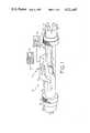
- FIG. 1is a perspective view, partly broken away, of a microwave plasma deposition system embodying the present invention for depositing amorphous semiconductor alloy films onto a receiving surface in layered form in accordance with the process of the invention;
- FIG. 2is a schematic representation of another system embodying the present invention adapted for exciting the reactioon gases separately and sequentially introducing the excited species to the receiving surface for layered deposition;
- FIG. 3is a sectional view of a tandem photovoltaic device which includes an intrinsic region comprising alternating layers of amorphous semiconductor alloys made by the process of the invention
- FIG. 4is a fragmentary sectional view of a photodetection device which includes a layered amorphous semiconductor alloy region made by the process of the invention.
- FIG. 5is a fragmentary sectional view of a xerographic drum including a layered amorphous semiconductor alloy region made by the process of the invention.
- a microwave deposition apparatussuitable for practicing the process of the present invention, is generally designated 10.
- the apparatus 10comprises a transparent tubular chamber or vessel 12 containing a substrate 14 having a receiving surface upon which the amorphous semiconductor alloy films are to be deposited.
- the substrateis heated by a heater 16 and the exterior of the chamber is irradiated by a moveable microwave energy source 17.
- Reaction gases passing from inlets 46 to an outlet 20 at opposite ends of the chamber 12receive microwave energy from the source 17.
- the combination of the reaction gases and the microwave energy from source 17causes the formation of a plasma.
- the plasmaalso moves resulting in the deposition of a film 22 having a layered structure.
- the reaction gasesinclude at least two reaction gases, each containing at least one alloying element to be deposited.
- the temperature of the substratecan be between room temperature and about 400 degrees Centigrade and the frequency of the microwave energy can be 2.45 Gigahertz and above and preferably 2.45 Gigahertz.
- the combined microwave energy and the reaction gasesform the plasma and as the source 17 is moved, the reaction gases are selectively excited to permit the deposition process of the layered materials to proceed.
- the film 22is spared from the damaging effects of ion bombardment because of the relatively low ion concentration in the plasma and reduced substrate self bias.
- the tubular chamber 12comprises a central quartz portion 24 and end portions 26 at opposite ends thereof.
- the end portions 26are closed by a pair of end fittings 30 and 32 to complete the chamber.
- Each of the end fittingsincludes a sleeve portion 34 extending from a closed end 36 to an open end portion.
- the open end portionis threaded to receive a collar 40 having an inwardly extending annular flange 42 at one end thereof.
- An o-ring(not shown) is confined in a space between the flange 42 and the end portion for compression thereof against the quartz portion 26.
- An air-tight sealis provided in this way between the end fittings 30 and 32 and the tubular chamber 12.
- the end fittings 30 and 32are preferably made of stainless steel or other suitable noncorrosive metal, with the closed ends 36 being welded or otherwise permanently joined to the sleeve portions 34.
- the closed end 36 of the end fitting 32is provided with gas inlets 46 through which the reaction gases are introduced into the vessel 12.
- An inert gassuch as argon can be introduced through one inlet 46 to assist in sustaining the plasma.
- the gas inlets 46are preferably connected to a conventional gas rack (not shown) for establishing regulated flows of reaction gases therein.
- the outlet 20is provided at the closed end 36 to the end fitting 30 for connection to selectable first and second pumps.
- the first pumpprovides for initial evacuation of the chamber.
- the second pumpprovides withdrawal of unused reaction gases during operation and maintenance of the proper deposition pressure of 0.1 Torr or greater.
- the microwave energy source 17preferably comprises a microwave energy generator 18 coupled to an antenna 19.
- the antenna 19is housed within a reflective housing 21 for concentration of the microwave energy into the chamber 12.
- the reflective housing 21is coupled to an antenna moving mechanism 23 adapted to move the housing 21 and antenna 19 back and forth in rectilinear movement as indicated by arrows 25.
- the movement of the antennain turn causes the plasma to move from a first position indicated at 27 to a second position indicated as 27'.
- the movement of the plasmais in the direction of flow of the reaction gases which flow from the inlets 46 to the outlet 20.
- the antenna as illustratedis a vertical antenna being preferably one-quarter wavelength long. The tip of the antenna just touches the outer surface of the vessel 12 to maximize transmission of its output to the reaction gases.
- the heaterpreferably comprises a conventional resistive heater contained within a substrate holder assembly 16. Power lines 17 for the heating element are passed through the closed end 36 of one of the end fittings.
- the system 10is first pumped down to below a desired deposition pressure, such as 10 -5 Torr.
- the reaction gasessuch as silicon tetrafluoride (SiF 4 ), or silane (SiH 4 ), and germane (GeH 4 ) or germanium tetrafluoride are fed into the separate inlet conduits 46 and chamber 12 is brought up to the desired operating pressure of, for example, 0.1 Torr.
- hydrogen (H 2 )can also be added.
- the microwave energy from the antenna 19is directed by the reflective housing 21 into the vessel 12 and the antenna 19 and housing 21 are moved as indicated to form a moving plasma over the substrate.
- the germanium containing gases(GeH 4 or GeF 4 ) have lower dissociation energies than the silicon containing gases (SiH 4 or SiF 4 ), they are selectively excited upon encountering the plasma zone resulting in a deposited amorphous semiconductor film which is initially germanium rich. As the gas mixture proceeds through the plasma zone and becomes more and more depleted of germanium containing excited species the remaining silicon containing excited species will result in the deposition of an amorphous semiconductor film which is silicon rich.
- the foregoing processcontinues resulting in alternating layers of amorphous germanium alloys and amorphous silicon alloys being deposited onto the substrate. Alternating layers of germanium rich and silicon rich alloys will result as long as the period of movement of the antenna 19 is long compared to the time necessary to deposit several atomic layers of the material.
- an amorphous semiconductor alloy film 22is deposited onto the substrate 14 having the aforementioned layered structure.
- the heater 16maintains the substrate at a temperature between about 20° Centigrade and 400° Centigrade.
- the output power of the microwave energy generator 18is adjusted between about 0.1 to 1 watt per cubic centimeter in power density.
- the flow rate of the reaction gasescan be between 1 to 10 SCCM for a two inch diameter reaction chamber 12. With the foregoing system parameters, deposition rates of 25 ⁇ to 250 ⁇ per second can be obtained.
- the process of the inventioncan be used for making photovoltaic devices.
- the resulting layered material of alternating layers of amorphous germanium alloys and amorphous silicon alloyscan be utilized as a narrow band gap region of a tandem photovoltaic cell.
- the other nonlayered intrinsic and doped regions of the devicecan be made by maintaining the antenna stationary and introducing appropriate reaction gases into the inlets 46.
- the reaction gasescan include germane (GeH 4 ), germanium tetrafluoride (GeF 4 ), silane (SiH 4 ) or silicon tetraflouride (SiF 4 ) and/or hydrogen.
- these reaction gasescan be combined depending upon desired properties.
- band gap increasing elementssuch as nitrogen or carbon can be added in the form of ammonia gas (NH 3 ) or methane gas (CH 4 ) if a wide band gap is desired.
- the doped regionscan be formed by introducing dopants into the vessel 12 for making the deposited film either p-type or n-type.
- dopantsfor example, diborane gas (B 2 H 6 ) to make a p-type film or phosphine gas (PH 3 ) to make an n-type film can be introduced through one of the inlets 46.
- the reaction gasescan be sequentially introduced to result in the formation of any desired device configuration.
- the system 50includes a substantially enclosed vessel or chamber 52 which contains the substrate 14 upon which the alloying elements are to be deposited in layered form.
- the system 50further includes a pair of microwave energy sources 54 and 56, a corresponding pair of "Woods horns" 58 and 60, and a switching circuit 62.
- the Woods horns 58 and 60each includes an inlet 58a and 60a respectively through which reaction gases can be fed.
- Reaction gasessuch as germanium tetrafluoride (GeF 4 ) or germane (GeH 4 ) can be fed into inlet 60a and reaction gases such as silicon tetrafluoride (SiF 4 ) or silane (SiH 4 ) can be fed into inlet 58a of horn 58 at flow rates of, for example, 15 sccm.
- the reaction gasesare selectively excited by the selected actuation of the microwave sources 56 and 54.
- the pressure within the chamber 52is maintained below the pressure within the Woods horns 58 and 60.
- one of the microwave sourcesfor example, source 56 is actuated.
- the microwave energy therefromexcites the reaction gas therein, such as germane to create germanium excited species which travel down the horn and strike the substrate 14 to deposit thereon a layer of amorphous germanium alloy.
- the other source 54is actuated to selectively and separately excite the reaction gas, such as silane (SiH 4 ) in horn 58 to cause a layer of amorphous silicon alloy to be deposited over the layer of amorphous germanium alloy. This process continues until enough alternating layers are deposited to provide a film of desired thickness. While alternative layers of amorphous silicon and germanium alloys are disclosed herein, it can be appreciated that any other alloying elements in gaseous form can also be deposited by using microwave energy in accordance with the present invention.
- FIG. 3it illustrates how the process of the present invention can be used in making a tandem photovoltaic cell, formed of a plurality of successive p-i-n regions including an amorphous semiconductor alloy and at least one region including a layered structure in accordance with the present invention.
- the tandem photovoltaic device 70includes a plurality of individual p-i-n type cells 72a, 72b, and 72c. Below the lowermost cell 72a is a substrate 71 which may be formed from a metallic material such as stainless steel, aluminum, tantalum, molybdenum, or chrome.
- the substrate 71 of the device 70 illustrated in FIG. 3includes a specular reflector 75.
- the specular reflector 75is formed from a reflective material by vapor depositing silver, gold, copper, chromium, molybdenum, or aluminum, for example, over the substrate 71. This form of reflector reflects light not absorbed during the initial pass through the active regions of the device back through the device and provides one additional pass therethrough. Since amorphous silicon or germanium alloys are good light absorbers, the one additional pass of the unabsorbed light through the device provides a significant increase in short circuit current and device efficiency.
- Each of the cells 72a, 72b and 72cincludes an n-type conductivity region 80a, 80b and 80c; an intrinsic region 78a, 78b and 78c; and a p-type conductivity region 76a, 76b and 76c.
- p-i-n cellsare illustrated, the present invention also pertains to multiple n-i-p cells as well.
- a further deposition processmay be either performed in a separate environment or as a part of a continuous process.
- a TCO (transparent conductive oxide) layer 82is added.
- An electrode grid 84may be added to the device where the cell is of a sufficiently large area, or if the conductivity of the TCO layer 82 is insufficient. The grid 84 shortens the carrier path and increases the collection efficiency.
- All of the amorphous semiconductor alloy regions, except region 78b, of the device 70 of FIG. 3can be formed by usng the apparatus of FIG. 1 while maintaining the antenna 19 in a stationary position over the substrate.
- the region 78bis an improved structure of alternating amorphous silicon and germanium alloys formed in the manner previously described with respect to FIG. 1. This structure combines the high transport properties of amorphous silicon alloys with the high photon absorption properties of amorphous germanium alloys.
- Amorphous germanium alloyshave a narrower band gap (about 1.1 eV) than amorphous silicon alloys (about 1.9 eV) but amorphous silicon alloys have shown to have a lower density of states than amorphous germanium alloys, and hence superior electrical transport properties.
- the layers of the alternating amorphous germanium and silicon alloyscan be made thin enough so that the amorphous germanium alloy layers can be utilized to absorb most of the photons for producing change carrier pairs and the amorphous silicon alloy layers can be utilized to effect transport of the charge carriers for efficient collection. Also, because the layers are thin, the entire region 78b can present a composite band gap between the extremes of 1.1 eV for amorphous germanium and 1.9 eV for amorphous silicon. This composite band gap is particularly appropriate for using such a layered structure as illustrated for the intrinsic region of the intermediate cell of a three cell tandem.
- FIG. 4there is illustrated another application of a layered amorphous semiconductor alloy region utilized in a photodetector device 90 whose resistance varies with the amount of light impinging thereon.
- An amorphous alloy body 92 thereofis deposited in accordance with the invention, has no p-n junctions and is located between a transparent electrode 94 and a substrate electrode 96.
- the amorphous alloy body 92has an undoped layered region 98 and doped non-layered regions 100 and 102 of the same conductivity type chosen to form a low resistance contact with the substrate 96 and the top electrode 94.
- the layered region 98preferably includes alternating layers of germanium and silicon amorphous alloys prepared by the methods previously described.
- an electrostatic image producing device 110(like a xerography drum) is illustrated.
- the device 110has a low dark conductivity, selective wavelength threshold, undoped or slightly p-doped amorphous oxygen stabilized layered amorphous semiconductor alloy region 112 deposited on a suitable substrate 114 such as a drum or belt.
- the layered region 112preferably includes alternating layers of amorphous silicon and germanium alloys prepared by the methods previously described. Small amounts of oxygen can be introduced into one or more of the layers by mixing small amounts of oxygen with the reaction gases.
- the alloy regions other than the intrinsic alloy regionscan be other than amorphous regions, such as polycrystalline regions.
- amorphousis meant an alloy or material which has long range disorder, although it may have short or intermediate order or even contain at times some crystalline inclusions.
Landscapes
- Chemical & Material Sciences (AREA)
- Engineering & Computer Science (AREA)
- General Chemical & Material Sciences (AREA)
- Chemical Kinetics & Catalysis (AREA)
- Materials Engineering (AREA)
- Mechanical Engineering (AREA)
- Metallurgy (AREA)
- Organic Chemistry (AREA)
- Physics & Mathematics (AREA)
- Plasma & Fusion (AREA)
- Photovoltaic Devices (AREA)
Abstract
Description
Claims (21)
Priority Applications (1)
| Application Number | Priority Date | Filing Date | Title |
|---|---|---|---|
| US06/565,033US4521447A (en) | 1982-10-18 | 1983-12-23 | Method and apparatus for making layered amorphous semiconductor alloys using microwave energy |
Applications Claiming Priority (2)
| Application Number | Priority Date | Filing Date | Title |
|---|---|---|---|
| US43506882A | 1982-10-18 | 1982-10-18 | |
| US06/565,033US4521447A (en) | 1982-10-18 | 1983-12-23 | Method and apparatus for making layered amorphous semiconductor alloys using microwave energy |
Related Parent Applications (1)
| Application Number | Title | Priority Date | Filing Date |
|---|---|---|---|
| US43506882ADivision | 1982-10-18 | 1982-10-18 |
Publications (1)
| Publication Number | Publication Date |
|---|---|
| US4521447Atrue US4521447A (en) | 1985-06-04 |
Family
ID=27030414
Family Applications (1)
| Application Number | Title | Priority Date | Filing Date |
|---|---|---|---|
| US06/565,033Expired - LifetimeUS4521447A (en) | 1982-10-18 | 1983-12-23 | Method and apparatus for making layered amorphous semiconductor alloys using microwave energy |
Country Status (1)
| Country | Link |
|---|---|
| US (1) | US4521447A (en) |
Cited By (48)
| Publication number | Priority date | Publication date | Assignee | Title |
|---|---|---|---|---|
| US4598164A (en)* | 1983-10-06 | 1986-07-01 | Exxon Research And Engineering Co. | Solar cell made from amorphous superlattice material |
| US4702934A (en)* | 1985-03-28 | 1987-10-27 | Canon Kabushiki Kaisha | Electrophotographic photosensitive member, process and apparatus for the preparation thereof |
| US4716048A (en)* | 1985-02-12 | 1987-12-29 | Canon Kabushiki Kaisha | Process for forming deposited film |
| US4717586A (en)* | 1985-02-18 | 1988-01-05 | Canon Kabushiki Kaisha | Process for forming deposited film |
| US4717585A (en)* | 1985-02-09 | 1988-01-05 | Canon Kabushiki Kaisha | Process for forming deposited film |
| DE3628443C1 (en)* | 1986-08-21 | 1988-02-11 | Dornier System Gmbh | Process for the production of amorphous layers |
| US4726963A (en)* | 1985-02-19 | 1988-02-23 | Canon Kabushiki Kaisha | Process for forming deposited film |
| US4756924A (en)* | 1984-11-05 | 1988-07-12 | Energy Conversion Devices, Inc. | Method for the microwave fabrication of boron doped semiconductor materials |
| US4759947A (en)* | 1984-10-08 | 1988-07-26 | Canon Kabushiki Kaisha | Method for forming deposition film using Si compound and active species from carbon and halogen compound |
| US4801468A (en)* | 1985-02-25 | 1989-01-31 | Canon Kabushiki Kaisha | Process for forming deposited film |
| US4803093A (en)* | 1985-03-27 | 1989-02-07 | Canon Kabushiki Kaisha | Process for preparing a functional deposited film |
| US4818560A (en)* | 1985-12-28 | 1989-04-04 | Canon Kabushiki Kaisha | Method for preparation of multi-layer structure film |
| US4818563A (en)* | 1985-02-21 | 1989-04-04 | Canon Kabushiki Kaisha | Process for forming deposited film |
| US4830890A (en)* | 1985-12-24 | 1989-05-16 | Canon Kabushiki Kaisha | Method for forming a deposited film from a gaseous silane compound heated on a substrate and introducing an active species therewith |
| US4835005A (en)* | 1983-08-16 | 1989-05-30 | Canon Kabushiki Kaishi | Process for forming deposition film |
| DE3741672A1 (en)* | 1987-12-09 | 1989-06-22 | Asea Brown Boveri | METHOD AND ARRANGEMENT FOR THE SURFACE TREATMENT OF SUBSTRATES |
| US4853251A (en)* | 1985-02-22 | 1989-08-01 | Canon Kabushiki Kaisha | Process for forming deposited film including carbon as a constituent element |
| US4857270A (en)* | 1987-05-19 | 1989-08-15 | Komatsu Electronic Metals Co., Ltd. | Process for manufacturing silicon-germanium alloys |
| US4891330A (en)* | 1987-07-27 | 1990-01-02 | Energy Conversion Devices, Inc. | Method of fabricating n-type and p-type microcrystalline semiconductor alloy material including band gap widening elements |
| US4948750A (en)* | 1988-03-24 | 1990-08-14 | Siemens Aktiengesellschaft | Method and apparatus for producing semiconductor layers composed of amorphous silicon-germanium alloys through glow discharge technique, particularly for solar cells |
| US5154135A (en)* | 1984-07-16 | 1992-10-13 | Canon Kabushiki Kaisha | Apparatus for forming a deposited film |
| US5244698A (en)* | 1985-02-21 | 1993-09-14 | Canon Kabushiki Kaisha | Process for forming deposited film |
| US5246744A (en)* | 1990-11-30 | 1993-09-21 | Central Glass Company, Limited | Method of forming thin film of amorphous silicon by plasma cvd |
| US5322568A (en)* | 1985-12-28 | 1994-06-21 | Canon Kabushiki Kaisha | Apparatus for forming deposited film |
| US5326716A (en)* | 1986-02-11 | 1994-07-05 | Max Planck-Gesellschaft Zur Foerderung Der Wissenschaften E.V. | Liquid phase epitaxial process for producing three-dimensional semiconductor structures by liquid phase expitaxy |
| WO1994026952A1 (en)* | 1993-05-14 | 1994-11-24 | Modular Process Technology Corporation | Apparatus and method for depositing diamond and refractory materials |
| US5591492A (en)* | 1986-04-11 | 1997-01-07 | Canon Kabushiki Kaisha | Process for forming and etching a film to effect specific crystal growth from activated species |
| US5633194A (en)* | 1995-04-18 | 1997-05-27 | The University Of Waterloo | Low temperature ion-beam assisted deposition methods for realizing SiGe/Si heterostructure |
| US5817559A (en)* | 1994-05-16 | 1998-10-06 | Matsushita Electric Industrial Co., Ltd. | Production method for a semiconductor device |
| US6010755A (en)* | 1996-06-06 | 2000-01-04 | Shimadzu Corporation | Method and apparatus for forming thin films using dual ECR plasma generators |
| US20040011465A1 (en)* | 2002-07-16 | 2004-01-22 | Tokyo Electron Limited | Plasma Processing apparatus |
| US6716725B1 (en)* | 1998-09-02 | 2004-04-06 | Tokyo Electron Limited | Plasma processing method and semiconductor device |
| US7547647B2 (en) | 2004-07-06 | 2009-06-16 | Hewlett-Packard Development Company, L.P. | Method of making a structure |
| US20090238998A1 (en)* | 2008-03-18 | 2009-09-24 | Applied Materials, Inc. | Coaxial microwave assisted deposition and etch systems |
| US20090238993A1 (en)* | 2008-03-19 | 2009-09-24 | Applied Materials, Inc. | Surface preheating treatment of plastics substrate |
| US20090277778A1 (en)* | 2008-05-06 | 2009-11-12 | Applied Materials, Inc. | Microwave rotatable sputtering deposition |
| US20090283400A1 (en)* | 2008-05-14 | 2009-11-19 | Applied Materials, Inc. | Microwave-assisted rotatable pvd |
| US20100078315A1 (en)* | 2008-09-26 | 2010-04-01 | Applied Materials, Inc. | Microstrip antenna assisted ipvd |
| US20100078320A1 (en)* | 2008-09-26 | 2010-04-01 | Applied Materials, Inc. | Microwave plasma containment shield shaping |
| US20100151149A1 (en)* | 2008-12-12 | 2010-06-17 | Ovshinsky Stanford R | Thin film deposition via a spatially-coordinated and time-synchronized process |
| US20110076420A1 (en)* | 2008-01-30 | 2011-03-31 | Applied Materials, Inc. | High efficiency low energy microwave ion/electron source |
| US20110076422A1 (en)* | 2008-01-30 | 2011-03-31 | Applied Materials, Inc. | Curved microwave plasma line source for coating of three-dimensional substrates |
| US8048782B1 (en) | 2010-08-12 | 2011-11-01 | Ovshinsky Innovation Llc | Plasma deposition of amorphous semiconductors at microwave frequencies |
| US8101245B1 (en) | 2010-08-12 | 2012-01-24 | Ovshinsky Innovation, Llc | Plasma deposition of amorphous semiconductors at microwave frequencies |
| US8222125B2 (en) | 2010-08-12 | 2012-07-17 | Ovshinsky Innovation, Llc | Plasma deposition of amorphous semiconductors at microwave frequencies |
| US20130312828A1 (en)* | 2012-05-24 | 2013-11-28 | International Business Machines Corporation | Photovoltaic device with band-stop filter |
| US8679594B2 (en) | 2008-02-20 | 2014-03-25 | Applied Materials, Inc. | Index modified coating on polymer substrate |
| US9018108B2 (en) | 2013-01-25 | 2015-04-28 | Applied Materials, Inc. | Low shrinkage dielectric films |
Citations (3)
| Publication number | Priority date | Publication date | Assignee | Title |
|---|---|---|---|---|
| GB2033355A (en)* | 1978-09-07 | 1980-05-21 | Standard Telephones Cables Ltd | Semiconductor processing |
| US4282267A (en)* | 1979-09-20 | 1981-08-04 | Western Electric Co., Inc. | Methods and apparatus for generating plasmas |
| US4379943A (en)* | 1981-12-14 | 1983-04-12 | Energy Conversion Devices, Inc. | Current enhanced photovoltaic device |
- 1983
- 1983-12-23USUS06/565,033patent/US4521447A/ennot_activeExpired - Lifetime
Patent Citations (3)
| Publication number | Priority date | Publication date | Assignee | Title |
|---|---|---|---|---|
| GB2033355A (en)* | 1978-09-07 | 1980-05-21 | Standard Telephones Cables Ltd | Semiconductor processing |
| US4282267A (en)* | 1979-09-20 | 1981-08-04 | Western Electric Co., Inc. | Methods and apparatus for generating plasmas |
| US4379943A (en)* | 1981-12-14 | 1983-04-12 | Energy Conversion Devices, Inc. | Current enhanced photovoltaic device |
Non-Patent Citations (5)
| Title |
|---|
| Brodsky, M. H. et al., IBM Technical Disclosure Bulletin, vol 22, No. 8A, Jan. 1980.* |
| C. Mailhiut et al., Electrical and Compositional Heterogeneity of Amorphous Si:H Films , Journal of Non Crystalline Solids, 35 & 36, pp. 207 212, 1980.* |
| C. Mailhiut et al., Electrical and Compositional Heterogeneity of Amorphous Si:H Films, Journal of Non-Crystalline Solids, 35 & 36, pp. 207-212, 1980. |
| Cohen, Charles, Thin Si Films Can Form at Room Temperature , Electronics, Nov. 3, 1981, pp. 82, 84.* |
| Cohen, Charles, Thin Si Films Can Form at Room Temperature, Electronics, Nov. 3, 1981, pp. 82, 84. |
Cited By (60)
| Publication number | Priority date | Publication date | Assignee | Title |
|---|---|---|---|---|
| US5645947A (en)* | 1983-08-16 | 1997-07-08 | Canon Kabushiki Kaisha | Silicon-containing deposited film |
| US4835005A (en)* | 1983-08-16 | 1989-05-30 | Canon Kabushiki Kaishi | Process for forming deposition film |
| US4598164A (en)* | 1983-10-06 | 1986-07-01 | Exxon Research And Engineering Co. | Solar cell made from amorphous superlattice material |
| US5154135A (en)* | 1984-07-16 | 1992-10-13 | Canon Kabushiki Kaisha | Apparatus for forming a deposited film |
| US4759947A (en)* | 1984-10-08 | 1988-07-26 | Canon Kabushiki Kaisha | Method for forming deposition film using Si compound and active species from carbon and halogen compound |
| US4756924A (en)* | 1984-11-05 | 1988-07-12 | Energy Conversion Devices, Inc. | Method for the microwave fabrication of boron doped semiconductor materials |
| US4717585A (en)* | 1985-02-09 | 1988-01-05 | Canon Kabushiki Kaisha | Process for forming deposited film |
| US4716048A (en)* | 1985-02-12 | 1987-12-29 | Canon Kabushiki Kaisha | Process for forming deposited film |
| US4717586A (en)* | 1985-02-18 | 1988-01-05 | Canon Kabushiki Kaisha | Process for forming deposited film |
| US4726963A (en)* | 1985-02-19 | 1988-02-23 | Canon Kabushiki Kaisha | Process for forming deposited film |
| US4818563A (en)* | 1985-02-21 | 1989-04-04 | Canon Kabushiki Kaisha | Process for forming deposited film |
| US5244698A (en)* | 1985-02-21 | 1993-09-14 | Canon Kabushiki Kaisha | Process for forming deposited film |
| US4853251A (en)* | 1985-02-22 | 1989-08-01 | Canon Kabushiki Kaisha | Process for forming deposited film including carbon as a constituent element |
| US4801468A (en)* | 1985-02-25 | 1989-01-31 | Canon Kabushiki Kaisha | Process for forming deposited film |
| US4803093A (en)* | 1985-03-27 | 1989-02-07 | Canon Kabushiki Kaisha | Process for preparing a functional deposited film |
| US4702934A (en)* | 1985-03-28 | 1987-10-27 | Canon Kabushiki Kaisha | Electrophotographic photosensitive member, process and apparatus for the preparation thereof |
| US4830890A (en)* | 1985-12-24 | 1989-05-16 | Canon Kabushiki Kaisha | Method for forming a deposited film from a gaseous silane compound heated on a substrate and introducing an active species therewith |
| US4818560A (en)* | 1985-12-28 | 1989-04-04 | Canon Kabushiki Kaisha | Method for preparation of multi-layer structure film |
| US5322568A (en)* | 1985-12-28 | 1994-06-21 | Canon Kabushiki Kaisha | Apparatus for forming deposited film |
| US5326716A (en)* | 1986-02-11 | 1994-07-05 | Max Planck-Gesellschaft Zur Foerderung Der Wissenschaften E.V. | Liquid phase epitaxial process for producing three-dimensional semiconductor structures by liquid phase expitaxy |
| US5397736A (en)* | 1986-02-11 | 1995-03-14 | Max-Planck-Gesellschaft Zur Foerderung Der Wissenschaften | Liquid epitaxial process for producing three-dimensional semiconductor structures |
| US5591492A (en)* | 1986-04-11 | 1997-01-07 | Canon Kabushiki Kaisha | Process for forming and etching a film to effect specific crystal growth from activated species |
| DE3628443C1 (en)* | 1986-08-21 | 1988-02-11 | Dornier System Gmbh | Process for the production of amorphous layers |
| US4857270A (en)* | 1987-05-19 | 1989-08-15 | Komatsu Electronic Metals Co., Ltd. | Process for manufacturing silicon-germanium alloys |
| US4891330A (en)* | 1987-07-27 | 1990-01-02 | Energy Conversion Devices, Inc. | Method of fabricating n-type and p-type microcrystalline semiconductor alloy material including band gap widening elements |
| DE3741672A1 (en)* | 1987-12-09 | 1989-06-22 | Asea Brown Boveri | METHOD AND ARRANGEMENT FOR THE SURFACE TREATMENT OF SUBSTRATES |
| US4948750A (en)* | 1988-03-24 | 1990-08-14 | Siemens Aktiengesellschaft | Method and apparatus for producing semiconductor layers composed of amorphous silicon-germanium alloys through glow discharge technique, particularly for solar cells |
| US5246744A (en)* | 1990-11-30 | 1993-09-21 | Central Glass Company, Limited | Method of forming thin film of amorphous silicon by plasma cvd |
| WO1994026952A1 (en)* | 1993-05-14 | 1994-11-24 | Modular Process Technology Corporation | Apparatus and method for depositing diamond and refractory materials |
| US5387288A (en)* | 1993-05-14 | 1995-02-07 | Modular Process Technology Corp. | Apparatus for depositing diamond and refractory materials comprising rotating antenna |
| US5817559A (en)* | 1994-05-16 | 1998-10-06 | Matsushita Electric Industrial Co., Ltd. | Production method for a semiconductor device |
| US6169004B1 (en) | 1994-05-16 | 2001-01-02 | Matsushita Electric Industrial Co., Ltd. | Production method for a semiconductor device |
| US5633194A (en)* | 1995-04-18 | 1997-05-27 | The University Of Waterloo | Low temperature ion-beam assisted deposition methods for realizing SiGe/Si heterostructure |
| US6010755A (en)* | 1996-06-06 | 2000-01-04 | Shimadzu Corporation | Method and apparatus for forming thin films using dual ECR plasma generators |
| US6716725B1 (en)* | 1998-09-02 | 2004-04-06 | Tokyo Electron Limited | Plasma processing method and semiconductor device |
| US20040011465A1 (en)* | 2002-07-16 | 2004-01-22 | Tokyo Electron Limited | Plasma Processing apparatus |
| US7547647B2 (en) | 2004-07-06 | 2009-06-16 | Hewlett-Packard Development Company, L.P. | Method of making a structure |
| US20090200541A1 (en)* | 2004-07-06 | 2009-08-13 | Hewlett-Packard Development Company Lp | Making a structure |
| US8143616B2 (en) | 2004-07-06 | 2012-03-27 | Oregon State University | Making a structure |
| US20110076420A1 (en)* | 2008-01-30 | 2011-03-31 | Applied Materials, Inc. | High efficiency low energy microwave ion/electron source |
| US20110097517A1 (en)* | 2008-01-30 | 2011-04-28 | Applied Materials, Inc. | Dynamic vertical microwave deposition of dielectric layers |
| US20110076422A1 (en)* | 2008-01-30 | 2011-03-31 | Applied Materials, Inc. | Curved microwave plasma line source for coating of three-dimensional substrates |
| US8679594B2 (en) | 2008-02-20 | 2014-03-25 | Applied Materials, Inc. | Index modified coating on polymer substrate |
| US20090238998A1 (en)* | 2008-03-18 | 2009-09-24 | Applied Materials, Inc. | Coaxial microwave assisted deposition and etch systems |
| US20090238993A1 (en)* | 2008-03-19 | 2009-09-24 | Applied Materials, Inc. | Surface preheating treatment of plastics substrate |
| US8057649B2 (en) | 2008-05-06 | 2011-11-15 | Applied Materials, Inc. | Microwave rotatable sputtering deposition |
| US20090277778A1 (en)* | 2008-05-06 | 2009-11-12 | Applied Materials, Inc. | Microwave rotatable sputtering deposition |
| US20090283400A1 (en)* | 2008-05-14 | 2009-11-19 | Applied Materials, Inc. | Microwave-assisted rotatable pvd |
| US8349156B2 (en) | 2008-05-14 | 2013-01-08 | Applied Materials, Inc. | Microwave-assisted rotatable PVD |
| US20100078320A1 (en)* | 2008-09-26 | 2010-04-01 | Applied Materials, Inc. | Microwave plasma containment shield shaping |
| US20100078315A1 (en)* | 2008-09-26 | 2010-04-01 | Applied Materials, Inc. | Microstrip antenna assisted ipvd |
| US20120263886A1 (en)* | 2008-12-12 | 2012-10-18 | Ovshinsky Stanford R | Thin Film Deposition via a Spatially-Coordinated and Time-Synchronized Process |
| US20100151149A1 (en)* | 2008-12-12 | 2010-06-17 | Ovshinsky Stanford R | Thin film deposition via a spatially-coordinated and time-synchronized process |
| US8168268B2 (en)* | 2008-12-12 | 2012-05-01 | Ovishinsky Innovation, LLC | Thin film deposition via a spatially-coordinated and time-synchronized process |
| US8048782B1 (en) | 2010-08-12 | 2011-11-01 | Ovshinsky Innovation Llc | Plasma deposition of amorphous semiconductors at microwave frequencies |
| US8222125B2 (en) | 2010-08-12 | 2012-07-17 | Ovshinsky Innovation, Llc | Plasma deposition of amorphous semiconductors at microwave frequencies |
| US8101245B1 (en) | 2010-08-12 | 2012-01-24 | Ovshinsky Innovation, Llc | Plasma deposition of amorphous semiconductors at microwave frequencies |
| US20130312828A1 (en)* | 2012-05-24 | 2013-11-28 | International Business Machines Corporation | Photovoltaic device with band-stop filter |
| US11908963B2 (en)* | 2012-05-24 | 2024-02-20 | Internationa Business Machines Corporation | Photovoltaic device with band-stop filter |
| US9018108B2 (en) | 2013-01-25 | 2015-04-28 | Applied Materials, Inc. | Low shrinkage dielectric films |
Similar Documents
| Publication | Publication Date | Title |
|---|---|---|
| US4521447A (en) | Method and apparatus for making layered amorphous semiconductor alloys using microwave energy | |
| EP0106698A2 (en) | Method and apparatus for making layered amorphous semiconductor alloys using microwave energy | |
| EP0104907B1 (en) | Method of making amorphous semiconductor alloys and devices using microwave energy | |
| US4615905A (en) | Method of depositing semiconductor films by free radical generation | |
| US4504518A (en) | Method of making amorphous semiconductor alloys and devices using microwave energy | |
| US4664937A (en) | Method of depositing semiconductor films by free radical generation | |
| US4379943A (en) | Current enhanced photovoltaic device | |
| US4619729A (en) | Microwave method of making semiconductor members | |
| US4522663A (en) | Method for optimizing photoresponsive amorphous alloys and devices | |
| US4342044A (en) | Method for optimizing photoresponsive amorphous alloys and devices | |
| EP0154160B1 (en) | Method and apparatus for making electrophotographic devices | |
| US4729341A (en) | Method and apparatus for making electrophotographic devices | |
| JPS58199710A (en) | P type amorphous oxygen and silicon alloy with improved wide band gap and application device | |
| EP0151754B1 (en) | An improved method of making a photoconductive member | |
| IE52207B1 (en) | Method of grading the band gaps of amorphous alloys and devices | |
| US4954182A (en) | Multiple cell photoresponsive amorphous photo voltaic devices including graded band gaps | |
| IE54573B1 (en) | Improved back reflector system and devices utilizing same | |
| GB2111534A (en) | Making photoresponsive amorphous alloys and devices by reactive plasma sputtering | |
| IE52208B1 (en) | Method for increasing the band gap in photoresponsive amorphous alloys and devices | |
| IE53485B1 (en) | Improved photoresponsive amorphous alloys | |
| US4469715A (en) | P-type semiconductor material having a wide band gap | |
| US4701343A (en) | Method of depositing thin films using microwave energy | |
| US4745000A (en) | Method of fabricating electrostatic drums using microwave energy | |
| US4715927A (en) | Improved method of making a photoconductive member | |
| GB2083703A (en) | Amorphous semiconductors |
Legal Events
| Date | Code | Title | Description |
|---|---|---|---|
| STCF | Information on status: patent grant | Free format text:PATENTED CASE | |
| AS | Assignment | Owner name:CANON INC., 30-2, SHIMOMARUKO 3-CHOME, OHTA-KU, TO Free format text:SECURITY INTEREST;ASSIGNOR:ENERGY CONVERSION DEVICES, INC;REEL/FRAME:004585/0577 Effective date:19860606 Owner name:CANON INC.,JAPAN Free format text:SECURITY INTEREST;ASSIGNOR:ENERGY CONVERSION DEVICES, INC;REEL/FRAME:004585/0577 Effective date:19860606 | |
| FPAY | Fee payment | Year of fee payment:4 | |
| AS | Assignment | Owner name:CANON INC., JAPAN Free format text:LICENSE;ASSIGNOR:ENERGY CONVERSION DEVICES, INC.;REEL/FRAME:005184/0012 Effective date:19870513 | |
| FEPP | Fee payment procedure | Free format text:PAYOR NUMBER ASSIGNED (ORIGINAL EVENT CODE: ASPN); ENTITY STATUS OF PATENT OWNER: LARGE ENTITY | |
| FPAY | Fee payment | Year of fee payment:8 | |
| AS | Assignment | Owner name:UNITED SOLAR SYSTEMS CORP., MICHIGAN Free format text:ASSIGNMENT OF ASSIGNORS INTEREST;ASSIGNOR:ENERGY CONVERSION DEVICES, INC.;REEL/FRAME:006969/0179 Effective date:19940414 | |
| FPAY | Fee payment | Year of fee payment:12 |