US4521443A - Integrated optical waveguide fabrication by ion implantation - Google Patents
Integrated optical waveguide fabrication by ion implantationDownload PDFInfo
- Publication number
- US4521443A US4521443AUS06/607,499US60749984AUS4521443AUS 4521443 AUS4521443 AUS 4521443AUS 60749984 AUS60749984 AUS 60749984AUS 4521443 AUS4521443 AUS 4521443A
- Authority
- US
- United States
- Prior art keywords
- substrate
- ions
- silicon dioxide
- index
- annealing
- Prior art date
- Legal status (The legal status is an assumption and is not a legal conclusion. Google has not performed a legal analysis and makes no representation as to the accuracy of the status listed.)
- Expired - Fee Related
Links
- 230000003287optical effectEffects0.000titleclaimsabstractdescription30
- 238000005468ion implantationMethods0.000titledescription6
- 238000004519manufacturing processMethods0.000titledescription3
- VYPSYNLAJGMNEJ-UHFFFAOYSA-NSilicium dioxideChemical compoundO=[Si]=OVYPSYNLAJGMNEJ-UHFFFAOYSA-N0.000claimsabstractdescription60
- 239000000758substrateSubstances0.000claimsabstractdescription44
- IJGRMHOSHXDMSA-UHFFFAOYSA-NnitrogenSubstancesN#NIJGRMHOSHXDMSA-UHFFFAOYSA-N0.000claimsabstractdescription35
- 229910052757nitrogenInorganic materials0.000claimsabstractdescription27
- 238000000034methodMethods0.000claimsabstractdescription24
- 239000000377silicon dioxideSubstances0.000claimsabstractdescription24
- 235000012239silicon dioxideNutrition0.000claimsabstractdescription22
- -1Nitrogen ionsChemical class0.000claimsabstractdescription20
- 238000010849ion bombardmentMethods0.000claimsabstractdescription9
- 150000002500ionsChemical class0.000claimsdescription11
- 238000010438heat treatmentMethods0.000claimsdescription6
- 229910021486amorphous silicon dioxideInorganic materials0.000claimsdescription3
- 239000007943implantSubstances0.000claimsdescription2
- 238000000137annealingMethods0.000abstractdescription22
- 239000000126substanceSubstances0.000abstractdescription9
- 230000003993interactionEffects0.000abstractdescription4
- 238000002513implantationMethods0.000description9
- XUIMIQQOPSSXEZ-UHFFFAOYSA-NSiliconChemical compound[Si]XUIMIQQOPSSXEZ-UHFFFAOYSA-N0.000description7
- 239000010703siliconSubstances0.000description7
- 239000005350fused silica glassSubstances0.000description6
- 229910052710siliconInorganic materials0.000description6
- 238000005056compactionMethods0.000description4
- 239000010410layerSubstances0.000description4
- 239000010453quartzSubstances0.000description4
- PCHJSUWPFVWCPO-UHFFFAOYSA-NgoldChemical compound[Au]PCHJSUWPFVWCPO-UHFFFAOYSA-N0.000description3
- 229910052737goldInorganic materials0.000description3
- 239000010931goldSubstances0.000description3
- 229910052814silicon oxideInorganic materials0.000description3
- 229910052581Si3N4Inorganic materials0.000description2
- 239000013078crystalSubstances0.000description2
- 230000000694effectsEffects0.000description2
- 229910001416lithium ionInorganic materials0.000description2
- 238000004377microelectronicMethods0.000description2
- HQVNEWCFYHHQES-UHFFFAOYSA-Nsilicon nitrideChemical compoundN12[Si]34N5[Si]62N3[Si]51N64HQVNEWCFYHHQES-UHFFFAOYSA-N0.000description2
- 239000002344surface layerSubstances0.000description2
- XFXPMWWXUTWYJX-UHFFFAOYSA-NCyanideChemical compoundN#[C-]XFXPMWWXUTWYJX-UHFFFAOYSA-N0.000description1
- HBBGRARXTFLTSG-UHFFFAOYSA-NLithium ionChemical compound[Li+]HBBGRARXTFLTSG-UHFFFAOYSA-N0.000description1
- 229910007277Si3 N4Inorganic materials0.000description1
- 229910052782aluminiumInorganic materials0.000description1
- XAGFODPZIPBFFR-UHFFFAOYSA-NaluminiumChemical compound[Al]XAGFODPZIPBFFR-UHFFFAOYSA-N0.000description1
- 239000011230binding agentSubstances0.000description1
- 229910052797bismuthInorganic materials0.000description1
- 229910052799carbonInorganic materials0.000description1
- 238000001311chemical methods and processMethods0.000description1
- 239000004020conductorSubstances0.000description1
- 230000007423decreaseEffects0.000description1
- 238000005516engineering processMethods0.000description1
- 238000005530etchingMethods0.000description1
- 239000011521glassSubstances0.000description1
- 229910052734heliumInorganic materials0.000description1
- 230000010354integrationEffects0.000description1
- 229910052744lithiumInorganic materials0.000description1
- 239000000463materialSubstances0.000description1
- 229910052760oxygenInorganic materials0.000description1
- 239000001301oxygenSubstances0.000description1
- 239000002245particleSubstances0.000description1
- 229910052698phosphorusInorganic materials0.000description1
- 230000001902propagating effectEffects0.000description1
- 230000005855radiationEffects0.000description1
Images
Classifications
- C—CHEMISTRY; METALLURGY
- C03—GLASS; MINERAL OR SLAG WOOL
- C03C—CHEMICAL COMPOSITION OF GLASSES, GLAZES OR VITREOUS ENAMELS; SURFACE TREATMENT OF GLASS; SURFACE TREATMENT OF FIBRES OR FILAMENTS MADE FROM GLASS, MINERALS OR SLAGS; JOINING GLASS TO GLASS OR OTHER MATERIALS
- C03C23/00—Other surface treatment of glass not in the form of fibres or filaments
- C03C23/0005—Other surface treatment of glass not in the form of fibres or filaments by irradiation
- C03C23/0055—Other surface treatment of glass not in the form of fibres or filaments by irradiation by ion implantation
- C—CHEMISTRY; METALLURGY
- C23—COATING METALLIC MATERIAL; COATING MATERIAL WITH METALLIC MATERIAL; CHEMICAL SURFACE TREATMENT; DIFFUSION TREATMENT OF METALLIC MATERIAL; COATING BY VACUUM EVAPORATION, BY SPUTTERING, BY ION IMPLANTATION OR BY CHEMICAL VAPOUR DEPOSITION, IN GENERAL; INHIBITING CORROSION OF METALLIC MATERIAL OR INCRUSTATION IN GENERAL
- C23C—COATING METALLIC MATERIAL; COATING MATERIAL WITH METALLIC MATERIAL; SURFACE TREATMENT OF METALLIC MATERIAL BY DIFFUSION INTO THE SURFACE, BY CHEMICAL CONVERSION OR SUBSTITUTION; COATING BY VACUUM EVAPORATION, BY SPUTTERING, BY ION IMPLANTATION OR BY CHEMICAL VAPOUR DEPOSITION, IN GENERAL
- C23C14/00—Coating by vacuum evaporation, by sputtering or by ion implantation of the coating forming material
- C23C14/22—Coating by vacuum evaporation, by sputtering or by ion implantation of the coating forming material characterised by the process of coating
- C23C14/48—Ion implantation
- G—PHYSICS
- G02—OPTICS
- G02B—OPTICAL ELEMENTS, SYSTEMS OR APPARATUS
- G02B6/00—Light guides; Structural details of arrangements comprising light guides and other optical elements, e.g. couplings
- G02B6/10—Light guides; Structural details of arrangements comprising light guides and other optical elements, e.g. couplings of the optical waveguide type
- G02B6/12—Light guides; Structural details of arrangements comprising light guides and other optical elements, e.g. couplings of the optical waveguide type of the integrated circuit kind
- G02B6/13—Integrated optical circuits characterised by the manufacturing method
- G02B6/134—Integrated optical circuits characterised by the manufacturing method by substitution by dopant atoms
- G02B6/1347—Integrated optical circuits characterised by the manufacturing method by substitution by dopant atoms using ion implantation
Definitions
- the present inventionrelates to a process using nitrogen ion implantation to increase the index of refraction near the surface of an amorphous silicon dioxide or glass substrate.
- the processis particularly suited for fabricating integrated optical waveguides and other integrated optical devices.
- the field of integrated opticsdeals with the miniaturization and integration of optical and electro-optical devices using technologies derived from the field of microelectronics. As compared with larger discrete optics, integrated optics allow devices to be constructed more cheaply and much more compactly, and it facilitates interfacing between optical and electronic components.
- Integrated optical devicesare fabricated by modifying the optical propagation characteristics of selected regions of an optically transmissive substrate.
- the basic building block of an integrated optical deviceis an optical waveguide whose function in integrated optics is somewhat analagous to that of a conductor in microelectronics.
- a waveguideis fabricated in a substrate by forming a channel having a higher index of refraction than the surrounding regions. Light propagating along the channel will be guided and confined within the channel because of total internal reflection at the channel boundaries.
- Amorphous silicon dioxidein the form of silica or fused quartz, is widely used as a substrate for fabricating integrated optical waveguides because it is highly transparent at visible and infrared wavelengths; i.e., it offers low attenuation to visible and infrared light.
- the following referencesillustrate the chronological development of the art of optical waveguide fabrication in silicon dioxide substrates.
- Standley, Gibson, and Rodgersreported in "Properties of Ion-Bombarded Fused Quartz for Integrated Optics," Applied Optics, vol. 11, pages 1313-1316, June 1972, that the index of refraction of fused quartz could be increased by ion bombardment. They suggested fabricating low-loss optical waveguides using ion bombardment to increase the index of refraction of a channel in a quartz substrate. Standley et al. investigated the changes in the index of refraction of fused quartz due to implantation by bombardment with ions of He, Li, C, P, Xe, Tl, and Bi.
- Standley et al.concluded that most of the increase in refractive index achieved by the bombardment could be removed by annealing, which annealing also significantly reduced the propagation losses. Although their data indicates that a small residual change in the index of refraction due to bombardment by lithium ions remained after annealing, they apparently attached little significance to this residual effect and attributed it to "partial" annealing.
- Standley et al.did not investigate the implantation of nitrogen ions. Also, they did not suggest that the changes caused by ion bombardment included significant chemical changes that might remain after annealing.
- Webb and Townsendsuggested that the greater change in the index of refraction for nitrogen implantation might be due to a chemical process rather than to the compaction process which was thought to have caused the increases in the index when the other ions were used.
- Webb and Townsendattributed the greater increase in refractive index achieved with nitrogen ion bombardment as being due to a chemical change, they made no suggestion that the propagation losses in the substrate could be reduced by annealing, nor did they suggest that a major portion of the change in the index of refraction due to nitrogen ion implantation would remain after annealing.
- Kerstenin U.S. Pat. No. 4,145,457, issued in 1979, disclosed a method for fabricating optical waveguides and directional couplers in quartz by implanting any one of a number of different ions, of which nitrogen was an example. Like Webb and Townsend, however, Kersten did not suggest the use of an annealing process to reduce the propagation loss in the waveguides, nor did he disclose that the nitrogen ions would produce a higher residual change in the index of refraction after annealing than the other ions considered.
- Hubler et aldisclosed in U.S. Pat. No. 4,262,056, issued in 1981, the use of nitrogen ions for bombarding a substrate to change the index of refraction for the purpose of fabricating a multilayer optical interference filter.
- the substrate material disclosed by Hublerwas silicon (Si) rather than silicon dioxide (SiO 2 ).
- Sisilicon
- SiO 2silicon dioxide
- Hubler et al.the implantation was performed at a high temperature of 600° C. to 1000° C. in order to cause the implanted ions to form silicon nitride (Si 3 N 4 ), and the substrate was maintained at this high temperature for a period of three to five hours during the implantation.
- Hubler et al.indicated that the high temperature removed the radiation damage to the crystallinity of the single-crystal layer of silicon overlying the implanted layer of silicon nitride, so that the optical properties of the overlying layer were unchanged from those of pure crystal and silicon.
- Hubler et al.did not discuss propagation losses in the implanted region or whether the high temperature affected such losses.
- Hubler et al.discloses that the nitrogen ion implantation of silicon substrates decreases the index of refraction in the implanted region, rather than increasing it as in the case of silicon dioxide substrates. This makes Hubler's process ill-suited to the fabrication of optical waveguides which require a channel having a higher refractive index than the surrounding substrate.
- Hubler's disclosed heating temperatures and timeswere applied to a silicon dioxide substrate rather than Hubler's disclosed silicon substrate, the heat would cause most of the implanted nitrogen ions to diffuse away from the implanted region, thus destroying the intended increase of the refractive index in that region.
- an optical waveguide or other optical deviceis fabricated by bombarding a substrate of silicon dioxide (silica or quartz) with nitrogen ions.
- the substrateis also annealed, preferably at 450 to 500 degrees Celsius for approximately thirty minutes, to remove most of the optical propagation loss introduced into the substrate by the compaction of or damage to the atomic structure caused by the bombardment.
- the annealing in this inventiondoes not significantly reduce the increase in the index of refraction achieved by the chemical interaction of the nitrogen ions with the silicon dioxide. The process can thus produce a low-loss optical waveguide.
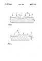
- FIG. 1depicts a planar waveguide
- FIG. 2depicts a two-dimensional waveguide, formed by the process of the present invention.
- a substrate 1is composed of silicon dioxide, preferably polished optical grade fused silica or fused quartz. Alternatively, a silicon dioxide layer over a silicon substrate could be substituted for the silicon dioxide substrate 1.
- the substrate 1is bombarded by nitrogen ions moving in the direction indicated by arrows 3. The nitrogen ions are implanted in region 2 near or adjacent to the surface of substrate 1.
- the index of refraction of region 2is raised above that of substrate 1.
- the increaseis caused both by compaction resulting from damage to the atomic structure of the substrate and by a chemical combination of the implanted nitrogen ions with the silicon dioxide. In the chemical interactions it is thought that some of the oxygen ions are replaced by the nitrogen ions so as to form nitrogen-doped silicon oxide (SiO x N y ).
- the ion bombardment energyis preferably 100 to 1000 KeV, and the dosage is preferably 1 ⁇ 10 16 to 3 ⁇ 10 17 ions per square centimeter. Lesser or greater energy levels may be used to obtain implantation nearer the surface or deeper into the substrate, and higher or lower bombardment dosages may be used to obtain greater or lesser changes in refractive index.
- substrate 1is annealed, preferably at 450 to 500 degrees Celsius, for a time period (preferably 30 minutes) sufficient to remove the damage to the atomic structure caused by the bombardment, thereby reducing the optical propagation losses in region 2.
- a higher temperaturemay be used for a shorter period of time, or a lower temperature for a longer period of time, to achieve the annealing.
- the annealing temperature and timesshould not be so excessive as to disturb the chemical interaction of the nitrogen ions with the silicon dioxide and thus destroy the increase in the refractive index achieved thereby.
- a substrate 1 with a region 2 near the surface having an increased index of refractionBoth the substrate and the surface layer exhibit low loss to optical waves.
- a low-loss substrate having a low-loss surface layer of increased index of refractionis desirable for use as an optical waveguide.
- a significant reduction in the optical waveguide lossis obtained by the annealing process. For example, in actual tests a planar waveguide exhibited a loss of 5 to 6 db per centimeter before annealing, while after annealing the loss was reduced to 0.1 db per centimeter.
- FIG. 2depicts a 2-dimensional channel waveguide.
- the silicon dioxide of substrate 4is bombarded by nitrogen ions moving in the direction of arrows 7 to implant the ions in channel 6 thus raising the index of refraction of the channel.
- a gold film 5approximately 2000 angstroms thick is deposited on substrate 4 using an aluminum binder film approximately 200 angstroms thick.
- the portion of gold film 5 covering channel 6is removed by standard photolithographic and etching processes in order to expose channel 6 to the ion bombardment.
- the gold maskis stripped in a cyanide etch, then the substrate is annealed in flowing nitrogen. A low-loss optical channel waveguide is produced by this process.
Landscapes
- Chemical & Material Sciences (AREA)
- Engineering & Computer Science (AREA)
- Physics & Mathematics (AREA)
- Organic Chemistry (AREA)
- Chemical Kinetics & Catalysis (AREA)
- Materials Engineering (AREA)
- Mechanical Engineering (AREA)
- Microelectronics & Electronic Packaging (AREA)
- Metallurgy (AREA)
- General Physics & Mathematics (AREA)
- Optics & Photonics (AREA)
- Plasma & Fusion (AREA)
- Health & Medical Sciences (AREA)
- Toxicology (AREA)
- Life Sciences & Earth Sciences (AREA)
- General Chemical & Material Sciences (AREA)
- Geochemistry & Mineralogy (AREA)
- Optical Integrated Circuits (AREA)
Abstract
Description
Claims (6)
Priority Applications (1)
| Application Number | Priority Date | Filing Date | Title |
|---|---|---|---|
| US06/607,499US4521443A (en) | 1984-05-07 | 1984-05-07 | Integrated optical waveguide fabrication by ion implantation |
Applications Claiming Priority (1)
| Application Number | Priority Date | Filing Date | Title |
|---|---|---|---|
| US06/607,499US4521443A (en) | 1984-05-07 | 1984-05-07 | Integrated optical waveguide fabrication by ion implantation |
Publications (1)
| Publication Number | Publication Date |
|---|---|
| US4521443Atrue US4521443A (en) | 1985-06-04 |
Family
ID=24432540
Family Applications (1)
| Application Number | Title | Priority Date | Filing Date |
|---|---|---|---|
| US06/607,499Expired - Fee RelatedUS4521443A (en) | 1984-05-07 | 1984-05-07 | Integrated optical waveguide fabrication by ion implantation |
Country Status (1)
| Country | Link |
|---|---|
| US (1) | US4521443A (en) |
Cited By (16)
| Publication number | Priority date | Publication date | Assignee | Title |
|---|---|---|---|---|
| US4592129A (en)* | 1985-04-01 | 1986-06-03 | Motorola, Inc. | Method of making an integral, multiple layer antireflection coating by hydrogen ion implantation |
| US5035916A (en)* | 1989-06-08 | 1991-07-30 | Northern Telecom Limited | Optical waveguide and method for its manufacture |
| US5066514A (en)* | 1989-01-26 | 1991-11-19 | Nippon Sheet Glass Co., Ltd. | Method of forming optical waveguides by ion implantation |
| GB2245379A (en)* | 1990-04-20 | 1992-01-02 | Nat Res Dev | Optical waveguide. |
| US5098792A (en)* | 1987-11-27 | 1992-03-24 | Societa Italiana Vetro - Siv - S.P.A. | Process for the manufacture of glass with modified radiant energy characteristics and the product so obtained |
| US5174876A (en)* | 1989-12-18 | 1992-12-29 | Forschungszentrum Julich Gmbh | Method of making an optical component by ion implantation |
| US5235662A (en)* | 1992-01-02 | 1993-08-10 | Eastman Kodak Company | Method to reduce light propagation losses in optical glasses and optical waveguide fabricated by same |
| WO2002088816A1 (en)* | 2001-04-27 | 2002-11-07 | Sarnoff Corporation | Optical waveguide crossing and method of making same |
| US6602558B1 (en)* | 1998-08-07 | 2003-08-05 | Toyota Jidosha Kabushiki Kaisha | Non-linear optical silica thin film manufacturing method and non-linear optical silica element |
| US20060210783A1 (en)* | 2005-03-18 | 2006-09-21 | Seder Thomas A | Coated article with anti-reflective coating and method of making same |
| US20060215952A1 (en)* | 2003-06-26 | 2006-09-28 | Mcintyre Thomas J | Integrated photonic circuits with vertical connections |
| US20110267512A1 (en)* | 2006-12-08 | 2011-11-03 | Sony Corporation | Solid-state image pickup device, method for manufacturing solid-state image pickup device, and camera |
| CN102707377A (en)* | 2012-06-12 | 2012-10-03 | 山东大学 | Method for preparing low-loss lithium niobate strip-shaped waveguide and branch structure |
| US9450053B2 (en) | 2012-07-26 | 2016-09-20 | Massachusetts Institute Of Technology | Photonic integrated circuits based on quantum cascade structures |
| US20170267571A1 (en)* | 2014-05-15 | 2017-09-21 | Corning Incorporated | Surface nitrided alkali-free glasses cross-reference to related applications |
| WO2018005327A1 (en)* | 2016-06-28 | 2018-01-04 | Corning Incorporated | Thin glass based article with high resistance to contact damage |
Citations (6)
| Publication number | Priority date | Publication date | Assignee | Title |
|---|---|---|---|---|
| US3562022A (en)* | 1967-12-26 | 1971-02-09 | Hughes Aircraft Co | Method of doping semiconductor bodies by indirection implantation |
| US4145457A (en)* | 1975-11-28 | 1979-03-20 | Siemens Aktiengesellschaft | Method for the production of optical directional couplers |
| US4262056A (en)* | 1978-09-15 | 1981-04-14 | The United States Of America As Represented By The Secretary Of The Navy | Ion-implanted multilayer optical interference filter |
| US4375312A (en)* | 1980-08-07 | 1983-03-01 | Hughes Aircraft Company | Graded index waveguide structure and process for forming same |
| US4411678A (en)* | 1981-04-02 | 1983-10-25 | Nippon Electric Co., Ltd. | Method for fabricating an optical waveguide on a planar glass substrate |
| US4465337A (en)* | 1982-03-05 | 1984-08-14 | Westinghouse Electric Corp. | Reduced reflectivity member and ion implantation method of fabrication |
- 1984
- 1984-05-07USUS06/607,499patent/US4521443A/ennot_activeExpired - Fee Related
Patent Citations (6)
| Publication number | Priority date | Publication date | Assignee | Title |
|---|---|---|---|---|
| US3562022A (en)* | 1967-12-26 | 1971-02-09 | Hughes Aircraft Co | Method of doping semiconductor bodies by indirection implantation |
| US4145457A (en)* | 1975-11-28 | 1979-03-20 | Siemens Aktiengesellschaft | Method for the production of optical directional couplers |
| US4262056A (en)* | 1978-09-15 | 1981-04-14 | The United States Of America As Represented By The Secretary Of The Navy | Ion-implanted multilayer optical interference filter |
| US4375312A (en)* | 1980-08-07 | 1983-03-01 | Hughes Aircraft Company | Graded index waveguide structure and process for forming same |
| US4411678A (en)* | 1981-04-02 | 1983-10-25 | Nippon Electric Co., Ltd. | Method for fabricating an optical waveguide on a planar glass substrate |
| US4465337A (en)* | 1982-03-05 | 1984-08-14 | Westinghouse Electric Corp. | Reduced reflectivity member and ion implantation method of fabrication |
Non-Patent Citations (4)
| Title |
|---|
| Standley et al., "Properties of Ion-Bombarded Fused Quartz for Integrated Optice", Applied Optics, vol. II, pp. 1313-1316, (Jun. 1972). |
| Standley et al., Properties of Ion Bombarded Fused Quartz for Integrated Optice , Applied Optics, vol. II, pp. 1313 1316, (Jun. 1972).* |
| Webb et al., "Refractive Index Profiles Induced by Ion Implantation Into Silica", J. Phys. D.: Applied Physics, vol. 9, pp. 1343-1354, (1976). |
| Webb et al., Refractive Index Profiles Induced by Ion Implantation Into Silica , J. Phys. D.: Applied Physics, vol. 9, pp. 1343 1354, (1976).* |
Cited By (26)
| Publication number | Priority date | Publication date | Assignee | Title |
|---|---|---|---|---|
| US4592129A (en)* | 1985-04-01 | 1986-06-03 | Motorola, Inc. | Method of making an integral, multiple layer antireflection coating by hydrogen ion implantation |
| US5098792A (en)* | 1987-11-27 | 1992-03-24 | Societa Italiana Vetro - Siv - S.P.A. | Process for the manufacture of glass with modified radiant energy characteristics and the product so obtained |
| US5066514A (en)* | 1989-01-26 | 1991-11-19 | Nippon Sheet Glass Co., Ltd. | Method of forming optical waveguides by ion implantation |
| US5035916A (en)* | 1989-06-08 | 1991-07-30 | Northern Telecom Limited | Optical waveguide and method for its manufacture |
| EP0401971A3 (en)* | 1989-06-08 | 1991-09-25 | Nortel Networks Corporation | Optical waveguide and method for its manufacture |
| US5174876A (en)* | 1989-12-18 | 1992-12-29 | Forschungszentrum Julich Gmbh | Method of making an optical component by ion implantation |
| GB2245379A (en)* | 1990-04-20 | 1992-01-02 | Nat Res Dev | Optical waveguide. |
| US5235662A (en)* | 1992-01-02 | 1993-08-10 | Eastman Kodak Company | Method to reduce light propagation losses in optical glasses and optical waveguide fabricated by same |
| US6602558B1 (en)* | 1998-08-07 | 2003-08-05 | Toyota Jidosha Kabushiki Kaisha | Non-linear optical silica thin film manufacturing method and non-linear optical silica element |
| WO2002088816A1 (en)* | 2001-04-27 | 2002-11-07 | Sarnoff Corporation | Optical waveguide crossing and method of making same |
| US6674950B2 (en) | 2001-04-27 | 2004-01-06 | Sarnoff Corporation | Optical waveguide crossing and method of making same |
| US20060215952A1 (en)* | 2003-06-26 | 2006-09-28 | Mcintyre Thomas J | Integrated photonic circuits with vertical connections |
| US7123787B1 (en)* | 2003-06-26 | 2006-10-17 | Bae Systems Information And Electronic Systems Integration Inc. | Integrated photonic circuits with vertical connections |
| US20060210783A1 (en)* | 2005-03-18 | 2006-09-21 | Seder Thomas A | Coated article with anti-reflective coating and method of making same |
| US8981275B2 (en)* | 2006-12-08 | 2015-03-17 | Sony Corporation | Solid-state image pickup device with an optical waveguide, method for manufacturing solid-state image pickup device, and camera |
| US20110267512A1 (en)* | 2006-12-08 | 2011-11-03 | Sony Corporation | Solid-state image pickup device, method for manufacturing solid-state image pickup device, and camera |
| US8525098B2 (en)* | 2006-12-08 | 2013-09-03 | Sony Corporation | Solid-state image pickup device, method for manufacturing solid-state image pickup device, and camera |
| CN102707377A (en)* | 2012-06-12 | 2012-10-03 | 山东大学 | Method for preparing low-loss lithium niobate strip-shaped waveguide and branch structure |
| CN102707377B (en)* | 2012-06-12 | 2014-04-16 | 山东大学 | Method for preparing low-loss lithium niobate strip-shaped waveguide and branch structure |
| US9450053B2 (en) | 2012-07-26 | 2016-09-20 | Massachusetts Institute Of Technology | Photonic integrated circuits based on quantum cascade structures |
| US9735549B2 (en) | 2012-07-26 | 2017-08-15 | Massachusetts Institute Of Technology | Methods for forming photonic integrated circuits based on quantum cascade structures |
| US20170267571A1 (en)* | 2014-05-15 | 2017-09-21 | Corning Incorporated | Surface nitrided alkali-free glasses cross-reference to related applications |
| WO2018005327A1 (en)* | 2016-06-28 | 2018-01-04 | Corning Incorporated | Thin glass based article with high resistance to contact damage |
| CN109689587A (en)* | 2016-06-28 | 2019-04-26 | 康宁股份有限公司 | The thin glass based articles damaged with high anti-contact |
| JP2019524613A (en)* | 2016-06-28 | 2019-09-05 | コーニング インコーポレイテッド | Thin glass-based article with high resistance to contact damage |
| US10612129B2 (en) | 2016-06-28 | 2020-04-07 | Corning Incorporated | Thin glass based article with high resistance to contact damage |
Similar Documents
| Publication | Publication Date | Title |
|---|---|---|
| US4521443A (en) | Integrated optical waveguide fabrication by ion implantation | |
| US4840816A (en) | Method of fabricating optical waveguides by ion implantation doping | |
| US5896484A (en) | Method of making a symmetrical optical waveguide | |
| GB2318647A (en) | Integrated optical waveguide polariser | |
| JP2006309222A (en) | Optical waveguide comprising quantum dot waveguide layer and manufacturing method therefor | |
| Noda et al. | Effect of Mg diffusion on Ti‐diffused LiNbO3 waveguides | |
| EP0401971B1 (en) | Optical waveguide and method for its manufacture | |
| JPS6375725A (en) | Planar type waveguide | |
| US4426440A (en) | Integrated optical grating device by thermal SiO2 growth on Si | |
| US20020048727A1 (en) | Method for forming a refractive-index-patterned film for use in optical device manufacturing | |
| JPH02275907A (en) | Formation of optical waveguide | |
| US3997687A (en) | Method of preparing optical waveguides | |
| JP3225878B2 (en) | Polymer waveguide and method of manufacturing the same | |
| US20030133638A1 (en) | Ion implanted lithium niobate modulator with reduced drift | |
| US6850672B2 (en) | Optical waveguide coupler and its characteristic adjusting method | |
| JP2004515815A (en) | Waveguide including channel on optical substrate | |
| CA2351090A1 (en) | Process for control of birefringence in waveguides | |
| EP0178815B1 (en) | Improvements relating to optical waveguides | |
| JPS5960405A (en) | Optical waveguide and its manufacturing method | |
| KR930010830B1 (en) | Method for manufacturing optical waveguide which prevents surface leach of lithium oxide during thermal diffusion | |
| Weiss et al. | Planar optical waveguides fabricated in LiNbO3 by multiple He+ implantations | |
| Buchal et al. | Ion implantation of optical ferroelectrics | |
| GB2394553A (en) | Raman optical waveguide with refractive index modified by ion implantation and fabrication method | |
| JPS5917510A (en) | optical waveguide | |
| Destefanis et al. | Optical waveguides in LiNbO3 formed by ion implantation |
Legal Events
| Date | Code | Title | Description |
|---|---|---|---|
| AS | Assignment | Owner name:NORTHROP CORPORATION, HAWTHORNE, CA. A CA CORP. Free format text:ASSIGNMENT OF ASSIGNORS INTEREST.;ASSIGNORS:NAIK, ISHVERLAL K.;EGUCHI, RONALD G.;REEL/FRAME:004258/0240 Effective date:19840504 Owner name:NORTHROP CORPORATION, A CA CORP., CALIFORNIA Free format text:ASSIGNMENT OF ASSIGNORS INTEREST;ASSIGNORS:NAIK, ISHVERLAL K.;EGUCHI, RONALD G.;REEL/FRAME:004258/0240 Effective date:19840504 | |
| CC | Certificate of correction | ||
| AS | Assignment | Owner name:NORTHROP CORPORATION, A DEL. CORP. Free format text:ASSIGNMENT OF ASSIGNORS INTEREST.;ASSIGNOR:NORTHROP CORPORATION, A CA. CORP.;REEL/FRAME:004634/0284 Effective date:19860516 | |
| FEPP | Fee payment procedure | Free format text:PAYOR NUMBER ASSIGNED (ORIGINAL EVENT CODE: ASPN); ENTITY STATUS OF PATENT OWNER: LARGE ENTITY | |
| FPAY | Fee payment | Year of fee payment:4 | |
| FPAY | Fee payment | Year of fee payment:8 | |
| FEPP | Fee payment procedure | Free format text:PAYER NUMBER DE-ASSIGNED (ORIGINAL EVENT CODE: RMPN); ENTITY STATUS OF PATENT OWNER: LARGE ENTITY Free format text:PAYOR NUMBER ASSIGNED (ORIGINAL EVENT CODE: ASPN); ENTITY STATUS OF PATENT OWNER: LARGE ENTITY | |
| REMI | Maintenance fee reminder mailed | ||
| LAPS | Lapse for failure to pay maintenance fees | ||
| FP | Lapsed due to failure to pay maintenance fee | Effective date:19970604 | |
| STCH | Information on status: patent discontinuation | Free format text:PATENT EXPIRED DUE TO NONPAYMENT OF MAINTENANCE FEES UNDER 37 CFR 1.362 |