US4513292A - Dipole radiating element - Google Patents
Dipole radiating elementDownload PDFInfo
- Publication number
- US4513292A US4513292AUS06/428,586US42858682AUS4513292AUS 4513292 AUS4513292 AUS 4513292AUS 42858682 AUS42858682 AUS 42858682AUS 4513292 AUS4513292 AUS 4513292A
- Authority
- US
- United States
- Prior art keywords
- section
- transmission line
- conductor
- sections
- slot
- Prior art date
- Legal status (The legal status is an assumption and is not a legal conclusion. Google has not performed a legal analysis and makes no representation as to the accuracy of the status listed.)
- Expired - Lifetime
Links
- 230000005540biological transmissionEffects0.000claimsabstractdescription52
- 239000004020conductorSubstances0.000claimsabstractdescription39
- 230000005855radiationEffects0.000claimsabstractdescription29
- 230000010287polarizationEffects0.000description5
- 238000003491arrayMethods0.000description4
- 230000004913activationEffects0.000description3
- 238000004519manufacturing processMethods0.000description3
- 239000007787solidSubstances0.000description3
- 239000000758substrateSubstances0.000description3
- 229910001369BrassInorganic materials0.000description1
- RYGMFSIKBFXOCR-UHFFFAOYSA-NCopperChemical compound[Cu]RYGMFSIKBFXOCR-UHFFFAOYSA-N0.000description1
- PNEYBMLMFCGWSK-UHFFFAOYSA-Naluminium oxideInorganic materials[O-2].[O-2].[O-2].[Al+3].[Al+3]PNEYBMLMFCGWSK-UHFFFAOYSA-N0.000description1
- 239000010951brassSubstances0.000description1
- 229910052802copperInorganic materials0.000description1
- 239000010949copperSubstances0.000description1
- 239000002184metalSubstances0.000description1
- 229910052751metalInorganic materials0.000description1
- 238000000034methodMethods0.000description1
- 238000003801millingMethods0.000description1
- 238000012986modificationMethods0.000description1
- 230000004048modificationEffects0.000description1
- 230000010363phase shiftEffects0.000description1
- 238000005476solderingMethods0.000description1
Images

Classifications
- H—ELECTRICITY
- H01—ELECTRIC ELEMENTS
- H01Q—ANTENNAS, i.e. RADIO AERIALS
- H01Q9/00—Electrically-short antennas having dimensions not more than twice the operating wavelength and consisting of conductive active radiating elements
- H01Q9/04—Resonant antennas
- H01Q9/16—Resonant antennas with feed intermediate between the extremities of the antenna, e.g. centre-fed dipole
- H01Q9/28—Conical, cylindrical, cage, strip, gauze, or like elements having an extended radiating surface; Elements comprising two conical surfaces having collinear axes and adjacent apices and fed by two-conductor transmission lines
- H01Q9/285—Planar dipole
- H—ELECTRICITY
- H01—ELECTRIC ELEMENTS
- H01Q—ANTENNAS, i.e. RADIO AERIALS
- H01Q21/00—Antenna arrays or systems
- H01Q21/06—Arrays of individually energised antenna units similarly polarised and spaced apart
- H01Q21/061—Two dimensional planar arrays
- H01Q21/062—Two dimensional planar arrays using dipole aerials
- H—ELECTRICITY
- H01—ELECTRIC ELEMENTS
- H01Q—ANTENNAS, i.e. RADIO AERIALS
- H01Q25/00—Antennas or antenna systems providing at least two radiating patterns
- H01Q25/001—Crossed polarisation dual antennas
Definitions
- the present inventionrelates to phased array antennas and more particularly to radiating elements useful in such arrays.
- Phased array antennasare known in which each element has an individual phase shifter associated with it.
- Waveguide horn elementswhich often employ gyromagnetic phase shifters, and radiating elements which are not of the horn type, which often employ solid state (e.g. diode) phase shifters, are two types of elements which may be used in such arrays.
- the solid state phase shifters and their associated radiating elementsare usually selected for array applications where low weight and/or low cost are primary selection criteria.
- Continuing development of array antennashas led to increasingly stringent overall performance specifications which require several thousand or more individual radiating elements in the antenna. These requirements have resulted in a corresponding increase in the complexity of those array elements and a tightening of fabrication tolerances for those elements. These combine to increase the cost of each element. For an array this cost increase is multiplied by the number of elements in the array.
- a radiating element suitable for use in a solid state type phased array antennais needed which has both the radiation characteristics required to meet high performance requirements and a structure which makes inexpensive fabrication possible.
- a radiating element in accordance with one embodiment of this inventioncomprises a one piece, wide, thin electrical conductor having first, second and third sections.
- the second sectionconnects the first section to the third section and spaces the first and third sections apart.
- the third sectioncomprises a dipole.
- a slot in the thin conductorseparates the second section into first and second spaced apart transmission line members.
- the portion of the third section which is adjacent the second sectionis separated by the slot into first and second spaced apart feed points of the dipole.
- the first and second feed pointsare connected directly to the first and second transmission line members, respectively.
- the element's first sectionconnects the first transmission line member to the second transmission line member at the ends of those members which are remote from the dipole feed points.
- the first section of the conductoris adapted for bonding to a feed circuit. When bonded to a feed circuit, the first section electrically couples the radiating element to that circuit and structurally supports the radiating element.
- Each of the sectionsis preferably substantially planar and the second and third sections are preferably disposed in a common plane.
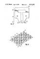
- FIG. 1is a plan view of a radiating element in accordance with the invention.
- FIG. 2is a perspective view of the element of FIG. 1 mounted on a microstrip feed circuit
- FIG. 3is a plan view of an alternative radiation element
- FIG. 4is a plan view of a modified form of the element of FIG. 3;
- FIG. 5is a perspective view of a planar array comprising elements like those in FIG. 3.
- a radiating element 10 in accordance with the inventionis illustrated in FIG. 1.
- the element 10is formed from a wide, thin, electrical conductor 12 which may preferably be sheet metal such as 0.02 inch (0.05 centimeter) thick brass or copper. This one piece element may be formed by stamping or milling.
- Element 10has first, second and third sections, 20, 30 and 40, respectively.
- a slot 14 through the thin dimension of the conductorextends from within the first section 20 through the second section 30 and the third section 40 to give the element 10 a generally U-shaped configuration.
- Slot 14has a wide foot portion 15 at its end which is within the first section (20) of element 10.
- the foot portion 15 of the slothas a generally circular periphery.
- the remainder of slot 14which may be referred to as a leg portion 16 is of substantially uniform width.
- the first section 20 of element 10comprises a balun member segment 22 formed from conductor 12.
- Balun member 22is adapted for bonding to a feed circuit where it becomes a portion of a transmission line. That transmission line is preferably an odd integer multiple of one-half wavelength (preferably 1/2 wavelength) long at a frequency near the middle of the designed operating frequency range of element 10.
- the second section 30 of element 10comprises a balanced transmission line and connects the first section 20 to the third section 40.
- the leg portion 16 of slot 14separates the section 30 into two spaced apart transmission line members 32 and 34 which together with the dielectric characteristics (air dielectric) of portion 16 of slot 14 form the balanced transmission line.
- the balun member 22connects the first transmission line member 32 to the second transmission line member 34.
- the portion of conductor 12 which comprises transmission line members 32 and 34 and balun member 22is of substantially constant width.
- the width of the leg portion 16 of slot 14is of the same order as the width of transmission line members 32 and 34.
- the third section 40 of element 10comprises a dipole radiator.
- the slot 14separates the dipole section 40 into two separate spaced apart dipole members 42 and 44.
- the transmission line members 32 and 34connect to dipole members 42 and 44, respectively at dipole feed points where sections 30 and 40 meet. These feed points are also spaced apart by slot 14.
- Each of the sections of the element 10is preferably planar and the second and third sections 30 and 40 are preferably disposed in a common plane. It is preferred to bend the element at the line 17 to place the first section 20 in a plane which is at a 90° angle to the common plane of the second and third sections.
- FIG. 2an element 10 in this bent configuration is illustrated bonded to a microstrip feed circuit 100 to form a module 120.
- the feed circuit 100includes an alumina substrate 102, having an upper major surface 104 (in FIG. 2).
- a ground plane 106covers the lower major surface.
- An unbalanced transmission line conductor 108, a balun member conductor 110 and phase control circuitry 112are disposed on the upper surface 104.
- Conductors 108 and 110each form a transmission line with the dielectric substrate 102 and the ground plane 106.
- Balun member 110preferably has the same outline as the balun segment 22 of element 10 in order that they may be soldered together to form a unitary structure.
- the transmission line formed by this unitary structure with dielectric 102 and conductor 106is the one mentioned above which is preferably 1/2 wavelength long.
- Conductor segment 22is preferably soldered along its entire length to the conductor 110.
- the unbalanced transmission line formed by conductor 108 and ground plane 106couples the phase shifter 112 to the balun and thus to element 10.
- An external signalmay be provided to phase shifter 112 by a transmission line 114.
- module 120can operate in a reflectarray mode in which a signal is received by element 10, transmitted to phase shifter 112 and reflected back to element 10 and radiated.
- the element 10is inexpensive to fabricate, is easily and reliably attached to the feed circuit 100 by soldering and provides the superior performance needed in modern phased arrays.
- the printed circuitry of feed circuit 100may be inexpensively fabricated using photolithographic techniques.
- the phase shiftermay be in accordance with U.S. Pat. No. 4,238,745 to Alfred Schwarzmann which is incorporated herein by reference.
- a plurality of modules 120may be positioned in a two dimensional array on a plane to form a planar phased array.
- the module 120 of FIG. 2accepts an unbalanced transmit signal from transmission line 114.
- This unbalanced signalis referenced to a ground potential which is applied to the ground plane 106.
- This signalmay be at a frequency at which balun 110 is one-half wavelength long.
- the phase shifting circuitry 112adjusts the phase of the transmit signal in accordance with the setting of its phase shifter control elements which may be diodes. From the phase shifter the signal propagates along the unbalanced transmission line comprised of the conductor 108 and the ground plane 106. This unbalanced signal on reaching the balun conductor 110 traverses the balun.
- the signals at points 36 and 38are one half cycle out of phase. These two signals comprise a balanced signal which propagates up the balanced transmission line formed by members 32 and 34. Upon reaching the dipole members 42 and 44 the signal is radiated into the surrounding medium.
- the module 120When the module 120 is used for reception of radiation signals, the module operates in a reciprocal manner.
- the radiation signalcouples to the dipole members 42 and 44, propagates down the transmission line formed by members 32 and 34 as a balanced signal and is converted to an unbalanced signal by the balun 110.
- This unbalanced signalpropagates along the unbalanced transmission line formed by conductor 108 and ground plane 106 to the phase shifter circuitry 112.
- Phase shifter circuitry 112impresses a phase shift on the received signal in accordance with the setting of the phase shifter. From there the signal propagates to a receiver or other utilization device or in a reflectarray is reflected back to element 10 for re-radiation.
- FIG. 3A modified version 200 of the element 10 is illustrated in FIG. 3.
- This elementis similar to element 10 in that it is a one piece radiating element formed from a single wide thin conductor (202).
- Element 200rather than having an open-ended slot 14 separating its second section into two spaced apart transmission line members, has a single closed ended slot or aperture 204 therein.
- the aperture 204is generally T-shaped with a cross bar portion 205 connected to an end of a leg portion 206.
- the leg portion 206 of the aperture 204has a non-uniform width.
- the widest portion of the legis a foot portion 207 at the end opposite from cross bar 205. Foot 207 is continuous with a lower leg portion 208 which is narrower than the foot.
- the lower leg 208is continuous with an upper leg portion 209 which connects to the cross bar portion 205.
- the upper leg 209is narrower than the lower leg 208.
- the upper and lower legs 209 and 208 of aperture 204together space apart the two transmission line members 232 and 234.
- the widths of the lower and upper legs 208 and 209,are selected to control electrical characteristics of the balanced transmission line which couples the first section 220 of the element to the dipole portion 240 of the element.
- portion 246 of the third section of element 200mechanically stiffens the element by tying the two sides 242 and 244 of the dipole portion together. This helps to prevent the two sides of the second and third sections of the element from being accidentally bent into a non-planar configuration. A bent-out-of-phase condition can occur more easily with element 10. Electrically, portion 246 makes the structure a folded dipole.
- the cross-bar portion 205 of aperture 204defines the size and shape of the inner periphery of this dipole. Thus the size and shape of the cross-bar portion 205 of the aperture controls the minimum size of the current loop of the folded dipole.
- the second section 230 of element 200(FIG. 3) has a generally trapezoidal outline and tapers from a relatively narrow base at the first section 220 to a relatively wide base at the third section 240. This taper aids in optimizing the overall radiation characteristics of the element 200 in the frequency range of operation. Dashed lines 239 are not physically present on element 200. They are to indicate the point where an extension of the tapering outer edge of section 230 reaches the outer edge of the element.
- the details of the configuration of the radiation element 200depend on the characteristics desired for the array for which it is designed. The details of element 200 also depend on its intended operating frequency range and the lattice or grid center-to-center spacing of adjacent modules in that array.
- the element of FIG. 3can be used in an array antenna having an operating frequency range of 3.1 to 3.5 GHz, in which the modules are positioned in a checkerboard grid configuration with module center-to-center spacings of about 3.5 inch in the x direction, a row-to-row spacing of about 1.0 inch in the Y direction and diagonal spacings of about 2.0 inches.
- FIG. 5would illustrate such an array if only the modules in the shaded squares were included. FIG. 5 will be discussed hereafter.
- the array for which element 200 is designedis specified to have sidelobes which are down about 25 dB from the main beam.
- the preferred dimensions of the radiation element 200are as indicated in the drawing where dimensions are in inches.
- the element 200At the center frequency (3.3 GHz) the element 200 has a height of about a quarter of a wavelength from the line 270 to the top of the element and has a width at the wide end of about 1.5 times its height.
- the radiation element 200 of FIG. 3is bent at a 90° angle along the dashed bend line 270 to dispose the second and third sections in a first plane and the first (balun member) section 220 in a second plane disposed at a 90° angle to the first plane when the element 200 is mounted on a feed circuit.
- radiation element 200 as illustrated in FIG. 3is preferred because of its superior radiation characteristics. However, other general configurations for the radiation element also provide useful results.
- the operation of the folded dipole 200 of FIG. 3is similar to the operation of element 10 in that it couples signals from the unbalanced transmission line formed by conductor 108 and ground plane 106 to the ambient environment and couples radiation from the ambient environment to that unbalanced transmission line.
- FIG. 4An alternative configuration for the folded dipole radiation element is shown generally at 300 in FIG. 4. Portions of element 300 which correspond to portions of element 200 have been given reference numbers in the 300's which have the same final two digits as the corresponding portion of element 200. Element 300 is substantially identical to the element 200 except that rather than having a closed T-shaped aperture 204, element 300 has a T-shaped slot 304 which is open at the foot of the T. Element 300 has two bonding tabs 326 and 328 instead of a semicircular balun member. Thus, in element 300 the first section 320 does not connect the two sides 332 and 334 of the balanced transmission line to each other.
- the configuration of the second and third sections 330 and 340are otherwise very similar to the configuration of the corresponding portions of the radiation element 200 in FIG. 2. Bonding of the tabs 326 and 328 to the balun member 110 of the microstrip circuit 100 such as the one shown in FIG. 3, will secure the radiation element 300 to the microstrip circuit 100. Minor modifications may need to be made in the balun member 110 to compensate for the lack of the additional layer of conductive material which the balun member 222 of radiation element 200 would have provided. Further, in the absence of the continuous balun member, the two transmission line members 332 and 334 are easily bent out of their common plane (prior to bonding). Therefore, if a planar configuration is desired, care must be taken to ensure that the second and third sections of element 300 remain planar at the time the tabs 326 and 328 are bonded to the microstrip circuit.
- the array 70 illustrated in FIG. 5is comprised of modules having elements 200 as their radiation members.
- the radiating elements 200are arranged in a checkerboard pattern.
- Modules 72 in the location of shaded squares of the checkerboardhave elements 200 having their width dimension aligned parallel to the x-axis 73 of the pattern.
- the modules 74 in the unshaded squares of the patternhave the width dimension of their elements aligned parallel to the y-axis 75 of the pattern.
- This element patterncorresponds to two separate arrays, each having a triangular grid, but rotated 90° with respect to each other and interlaced to place the elements of one grid in the gaps in the other grid. Activation of just the modules in the shaded squares produces a first polarization radiation.
- Activation of just the modules in the unshaded squaresproduces radiation having a polarization at 90° to the first polarization.
- Activation of both sets of modulescan produce any desired polarization by appropriate relative phase and amplitude control. For reception this array can respond to all radiation polarizations.
Landscapes
- Variable-Direction Aerials And Aerial Arrays (AREA)
Abstract
Description
Claims (8)
Priority Applications (1)
| Application Number | Priority Date | Filing Date | Title |
|---|---|---|---|
| US06/428,586US4513292A (en) | 1982-09-30 | 1982-09-30 | Dipole radiating element |
Applications Claiming Priority (1)
| Application Number | Priority Date | Filing Date | Title |
|---|---|---|---|
| US06/428,586US4513292A (en) | 1982-09-30 | 1982-09-30 | Dipole radiating element |
Publications (1)
| Publication Number | Publication Date |
|---|---|
| US4513292Atrue US4513292A (en) | 1985-04-23 |
Family
ID=23699546
Family Applications (1)
| Application Number | Title | Priority Date | Filing Date |
|---|---|---|---|
| US06/428,586Expired - LifetimeUS4513292A (en) | 1982-09-30 | 1982-09-30 | Dipole radiating element |
Country Status (1)
| Country | Link |
|---|---|
| US (1) | US4513292A (en) |
Cited By (39)
| Publication number | Priority date | Publication date | Assignee | Title |
|---|---|---|---|---|
| EP0249303A1 (en)* | 1986-05-28 | 1987-12-16 | THE GENERAL ELECTRIC COMPANY, p.l.c. | A dipole array |
| US4737797A (en)* | 1986-06-26 | 1988-04-12 | Motorola, Inc. | Microstrip balun-antenna apparatus |
| US4847626A (en)* | 1987-07-01 | 1989-07-11 | Motorola, Inc. | Microstrip balun-antenna |
| US5070340A (en)* | 1989-07-06 | 1991-12-03 | Ball Corporation | Broadband microstrip-fed antenna |
| FR2685822A1 (en)* | 1991-12-31 | 1993-07-02 | Thomson Csf | PHASE CONTROL REFLECTIVE ARRAY. |
| WO1994018719A1 (en)* | 1993-02-02 | 1994-08-18 | Kathrein-Werke Kg | Directional antenna, in particular a dipole antenna |
| EP0626736A1 (en)* | 1993-05-25 | 1994-11-30 | Société dite CEIS TM (Société Anonyme) | Omnidirectional radio frequency antenna and its application in a radar transponder |
| US5691735A (en)* | 1992-08-07 | 1997-11-25 | Butland; Roger John | Dipole antenna having coupling tabs |
| US5781159A (en)* | 1996-09-27 | 1998-07-14 | Boeing North American, Inc. | Planar antenna with integral impedance matching |
| US6031504A (en)* | 1998-06-10 | 2000-02-29 | Mcewan; Thomas E. | Broadband antenna pair with low mutual coupling |
| US6046704A (en)* | 1999-01-06 | 2000-04-04 | Marconi Aerospace Systems Inc. Advanced Systems Division | Stamp-and-bend double-tuned radiating elements and antennas |
| US6072439A (en)* | 1998-01-15 | 2000-06-06 | Andrew Corporation | Base station antenna for dual polarization |
| US20050110698A1 (en)* | 2003-11-24 | 2005-05-26 | Sandbridge Technologies Inc. | Modified printed dipole antennas for wireless multi-band communication systems |
| US20060208955A1 (en)* | 2005-03-17 | 2006-09-21 | Fujitsu Limited | Tag antenna |
| US20060214867A1 (en)* | 2005-03-23 | 2006-09-28 | Tai-Lee Chen | Shaped dipole antenna |
| US20060273865A1 (en)* | 2005-06-02 | 2006-12-07 | Timofeev Igor E | Dipole antenna array |
| GB2430307A (en)* | 2005-09-19 | 2007-03-21 | Antenova Ltd | Compact balanced antenna arrangement |
| US20090207092A1 (en)* | 2008-02-15 | 2009-08-20 | Paul Nysen | Compact diversity antenna system |
| US7932862B2 (en)* | 2008-04-01 | 2011-04-26 | Quanta Computer, Inc. | Antenna for a wireless personal area network and a wireless local area network |
| US20110187363A1 (en)* | 2010-01-29 | 2011-08-04 | Bae Systems Information And Electronic Systems Integration Inc. | Method and apparatus for sensing the presence of explosives, contraband and other molecules using nuclear quadrupole resonance |
| JP2012253423A (en)* | 2011-05-31 | 2012-12-20 | Nissei Ltd | PCB antenna |
| US20130069837A1 (en)* | 2010-06-09 | 2013-03-21 | Galtronics Corporation Ltd. | Directive antenna with isolation feature |
| US20130088304A1 (en)* | 2010-06-30 | 2013-04-11 | Bae Systems Plc | Antenna feed structure |
| US8463557B2 (en) | 2010-02-18 | 2013-06-11 | Bae Systems Information And Electronic Systems Integration Inc. | Method and system for the detection and identification of explosives and/or contraband |
| US8570038B2 (en) | 2010-01-29 | 2013-10-29 | R.A. Miller Industries, Inc. | Long range detection of explosives or contraband using nuclear quadrupole resonance |
| US8654031B2 (en) | 2010-09-28 | 2014-02-18 | Raytheon Company | Plug-in antenna |
| US8674697B2 (en) | 2010-01-29 | 2014-03-18 | R.A. Miller Industries, Inc. | Long distance explosive detection using nuclear quadrupole resonance and one or more monopoles |
| US8710837B2 (en) | 2010-01-29 | 2014-04-29 | Bae Systems Information And Electronic Systems Integration Inc. | Shipping container explosives and contraband detection system using nuclear quadrupole resonance |
| US8773127B2 (en) | 2010-01-29 | 2014-07-08 | R.A. Miller Industries, Inc. | Transmission line array for explosive detection using nuclear quadrupole resonance |
| US20150077303A1 (en)* | 2013-09-13 | 2015-03-19 | Sercomm Corporation | Antenna structure and electronic device using the same |
| US9476953B1 (en) | 2012-08-24 | 2016-10-25 | Bae Systems Information And Electronic Systems Integration Inc. | Nuclear quadrupole resonance system |
| US20180115087A1 (en)* | 2016-10-26 | 2018-04-26 | Movandi Corporation | Phased Array Antenna Panel with Configurable Slanted Antenna Rows |
| RU2657091C1 (en)* | 2017-05-19 | 2018-06-08 | Акционерное общество "Научно-производственное объединение "Лианозовский электромеханический завод" | Flat broadband vibrator |
| US20180219628A1 (en)* | 2017-01-31 | 2018-08-02 | Samsung Electronics Co., Ltd. | High-frequency signal transmission/reception device |
| CN110199438A (en)* | 2017-01-20 | 2019-09-03 | 索尼半导体解决方案公司 | Antenna and receiver |
| RU2752288C2 (en)* | 2018-08-14 | 2021-07-26 | Публичное акционерное общество "Научно-производственное объединение "Алмаз" имени академика А.А.Расплетина" (ПАО "НПО Алмаз") | Dual-band emitter for antenna array |
| CN113437488A (en)* | 2021-06-07 | 2021-09-24 | 京信通信技术(广州)有限公司 | Multi-frequency array antenna, radiation structure and assembly method of radiation structure |
| US20220021108A1 (en)* | 2019-04-01 | 2022-01-20 | Samsung Electronics Co., Ltd. | Radiating element of antenna and antenna |
| CN114221125A (en)* | 2021-12-22 | 2022-03-22 | 京信通信技术(广州)有限公司 | Integrated antenna unit and antenna device |
Citations (17)
| Publication number | Priority date | Publication date | Assignee | Title |
|---|---|---|---|---|
| US2507528A (en)* | 1945-08-13 | 1950-05-16 | Standard Telephones Cables Ltd | Antenna |
| DE861114C (en)* | 1951-10-11 | 1952-12-29 | Max Grundig | Built-in antennas for TV and VHF receivers |
| US2978703A (en)* | 1960-03-08 | 1961-04-04 | Avco Corp | Folded dipole antenna fabricated from a single metallic sheet |
| US3488657A (en)* | 1965-10-18 | 1970-01-06 | Bendix Corp | Low profile antenna |
| US3587110A (en)* | 1969-07-01 | 1971-06-22 | Rca Corp | Corporate-network printed antenna system |
| DE2020195A1 (en)* | 1970-04-25 | 1971-11-11 | Collis & Sons Ltd J | Conveyor roller and roller conveyor formed from it |
| US3623112A (en)* | 1969-12-19 | 1971-11-23 | Bendix Corp | Combined dipole and waveguide radiator for phased antenna array |
| US3678418A (en)* | 1971-07-28 | 1972-07-18 | Rca Corp | Printed circuit balun |
| US3805269A (en)* | 1971-06-14 | 1974-04-16 | Matsushita Electric Industrial Co Ltd | Diverse type dipole antennas on common mount |
| DE2325704A1 (en)* | 1973-05-21 | 1974-12-19 | Siemens Ag | DIRECTIONAL ANTENNA |
| US4001834A (en)* | 1975-04-08 | 1977-01-04 | Aeronutronic Ford Corporation | Printed wiring antenna and arrays fabricated thereof |
| CA1003559A (en)* | 1974-06-10 | 1977-01-11 | Thomas E. Manwarren | Stripline slotted balun dipole antenna |
| US4035807A (en)* | 1974-12-23 | 1977-07-12 | Hughes Aircraft Company | Integrated microwave phase shifter and radiator module |
| US4042935A (en)* | 1974-08-01 | 1977-08-16 | Hughes Aircraft Company | Wideband multiplexing antenna feed employing cavity backed wing dipoles |
| US4084162A (en)* | 1975-05-15 | 1978-04-11 | Etat Francais Represented By Delegation Ministerielle Pour L'armement | Folded back doublet microstrip antenna |
| US4238745A (en)* | 1979-06-18 | 1980-12-09 | Rca Corporation | Phase shifter |
| US4284868A (en)* | 1978-12-21 | 1981-08-18 | Amana Refrigeration, Inc. | Microwave oven |
- 1982
- 1982-09-30USUS06/428,586patent/US4513292A/ennot_activeExpired - Lifetime
Patent Citations (17)
| Publication number | Priority date | Publication date | Assignee | Title |
|---|---|---|---|---|
| US2507528A (en)* | 1945-08-13 | 1950-05-16 | Standard Telephones Cables Ltd | Antenna |
| DE861114C (en)* | 1951-10-11 | 1952-12-29 | Max Grundig | Built-in antennas for TV and VHF receivers |
| US2978703A (en)* | 1960-03-08 | 1961-04-04 | Avco Corp | Folded dipole antenna fabricated from a single metallic sheet |
| US3488657A (en)* | 1965-10-18 | 1970-01-06 | Bendix Corp | Low profile antenna |
| US3587110A (en)* | 1969-07-01 | 1971-06-22 | Rca Corp | Corporate-network printed antenna system |
| US3623112A (en)* | 1969-12-19 | 1971-11-23 | Bendix Corp | Combined dipole and waveguide radiator for phased antenna array |
| DE2020195A1 (en)* | 1970-04-25 | 1971-11-11 | Collis & Sons Ltd J | Conveyor roller and roller conveyor formed from it |
| US3805269A (en)* | 1971-06-14 | 1974-04-16 | Matsushita Electric Industrial Co Ltd | Diverse type dipole antennas on common mount |
| US3678418A (en)* | 1971-07-28 | 1972-07-18 | Rca Corp | Printed circuit balun |
| DE2325704A1 (en)* | 1973-05-21 | 1974-12-19 | Siemens Ag | DIRECTIONAL ANTENNA |
| CA1003559A (en)* | 1974-06-10 | 1977-01-11 | Thomas E. Manwarren | Stripline slotted balun dipole antenna |
| US4042935A (en)* | 1974-08-01 | 1977-08-16 | Hughes Aircraft Company | Wideband multiplexing antenna feed employing cavity backed wing dipoles |
| US4035807A (en)* | 1974-12-23 | 1977-07-12 | Hughes Aircraft Company | Integrated microwave phase shifter and radiator module |
| US4001834A (en)* | 1975-04-08 | 1977-01-04 | Aeronutronic Ford Corporation | Printed wiring antenna and arrays fabricated thereof |
| US4084162A (en)* | 1975-05-15 | 1978-04-11 | Etat Francais Represented By Delegation Ministerielle Pour L'armement | Folded back doublet microstrip antenna |
| US4284868A (en)* | 1978-12-21 | 1981-08-18 | Amana Refrigeration, Inc. | Microwave oven |
| US4238745A (en)* | 1979-06-18 | 1980-12-09 | Rca Corporation | Phase shifter |
Cited By (56)
| Publication number | Priority date | Publication date | Assignee | Title |
|---|---|---|---|---|
| EP0249303A1 (en)* | 1986-05-28 | 1987-12-16 | THE GENERAL ELECTRIC COMPANY, p.l.c. | A dipole array |
| US4737797A (en)* | 1986-06-26 | 1988-04-12 | Motorola, Inc. | Microstrip balun-antenna apparatus |
| US4847626A (en)* | 1987-07-01 | 1989-07-11 | Motorola, Inc. | Microstrip balun-antenna |
| US5070340A (en)* | 1989-07-06 | 1991-12-03 | Ball Corporation | Broadband microstrip-fed antenna |
| FR2685822A1 (en)* | 1991-12-31 | 1993-07-02 | Thomson Csf | PHASE CONTROL REFLECTIVE ARRAY. |
| EP0551780A1 (en)* | 1991-12-31 | 1993-07-21 | Thomson-Csf | A phase controlled reflector antenna array |
| US5691735A (en)* | 1992-08-07 | 1997-11-25 | Butland; Roger John | Dipole antenna having coupling tabs |
| WO1994018719A1 (en)* | 1993-02-02 | 1994-08-18 | Kathrein-Werke Kg | Directional antenna, in particular a dipole antenna |
| EP0626736A1 (en)* | 1993-05-25 | 1994-11-30 | Société dite CEIS TM (Société Anonyme) | Omnidirectional radio frequency antenna and its application in a radar transponder |
| FR2705836A1 (en)* | 1993-05-25 | 1994-12-02 | Ceis Tm | An omnidirectional radio antenna and its application to a radar responder. |
| US5781159A (en)* | 1996-09-27 | 1998-07-14 | Boeing North American, Inc. | Planar antenna with integral impedance matching |
| US6072439A (en)* | 1998-01-15 | 2000-06-06 | Andrew Corporation | Base station antenna for dual polarization |
| US6031504A (en)* | 1998-06-10 | 2000-02-29 | Mcewan; Thomas E. | Broadband antenna pair with low mutual coupling |
| US6046704A (en)* | 1999-01-06 | 2000-04-04 | Marconi Aerospace Systems Inc. Advanced Systems Division | Stamp-and-bend double-tuned radiating elements and antennas |
| US20050110698A1 (en)* | 2003-11-24 | 2005-05-26 | Sandbridge Technologies Inc. | Modified printed dipole antennas for wireless multi-band communication systems |
| US20060208956A1 (en)* | 2003-11-24 | 2006-09-21 | Emanoil Surducan | Modified printed dipole antennas for wireless multi-band communication systems |
| US7095382B2 (en)* | 2003-11-24 | 2006-08-22 | Sandbridge Technologies, Inc. | Modified printed dipole antennas for wireless multi-band communications systems |
| US7659863B2 (en)* | 2005-03-17 | 2010-02-09 | Fujitsu Limited | Tag antenna |
| US20060208955A1 (en)* | 2005-03-17 | 2006-09-21 | Fujitsu Limited | Tag antenna |
| US20070268194A1 (en)* | 2005-03-17 | 2007-11-22 | Fujitsu Limited | Tag antenna |
| US20060214867A1 (en)* | 2005-03-23 | 2006-09-28 | Tai-Lee Chen | Shaped dipole antenna |
| US7129904B2 (en)* | 2005-03-23 | 2006-10-31 | Uspec Technology Co., Ltd. | Shaped dipole antenna |
| US20060273865A1 (en)* | 2005-06-02 | 2006-12-07 | Timofeev Igor E | Dipole antenna array |
| US7639198B2 (en)* | 2005-06-02 | 2009-12-29 | Andrew Llc | Dipole antenna array having dipole arms tilted at an acute angle |
| GB2430307A (en)* | 2005-09-19 | 2007-03-21 | Antenova Ltd | Compact balanced antenna arrangement |
| US20080238800A1 (en)* | 2005-09-19 | 2008-10-02 | Brian Collins | Balanced Antenna Devices |
| US20090207092A1 (en)* | 2008-02-15 | 2009-08-20 | Paul Nysen | Compact diversity antenna system |
| US7724201B2 (en)* | 2008-02-15 | 2010-05-25 | Sierra Wireless, Inc. | Compact diversity antenna system |
| US7932862B2 (en)* | 2008-04-01 | 2011-04-26 | Quanta Computer, Inc. | Antenna for a wireless personal area network and a wireless local area network |
| US8773127B2 (en) | 2010-01-29 | 2014-07-08 | R.A. Miller Industries, Inc. | Transmission line array for explosive detection using nuclear quadrupole resonance |
| US8570038B2 (en) | 2010-01-29 | 2013-10-29 | R.A. Miller Industries, Inc. | Long range detection of explosives or contraband using nuclear quadrupole resonance |
| US20110187363A1 (en)* | 2010-01-29 | 2011-08-04 | Bae Systems Information And Electronic Systems Integration Inc. | Method and apparatus for sensing the presence of explosives, contraband and other molecules using nuclear quadrupole resonance |
| US8674697B2 (en) | 2010-01-29 | 2014-03-18 | R.A. Miller Industries, Inc. | Long distance explosive detection using nuclear quadrupole resonance and one or more monopoles |
| US8710837B2 (en) | 2010-01-29 | 2014-04-29 | Bae Systems Information And Electronic Systems Integration Inc. | Shipping container explosives and contraband detection system using nuclear quadrupole resonance |
| US8742753B2 (en) | 2010-01-29 | 2014-06-03 | R.A. Miller Industries, Inc. | Method and apparatus for sensing the presence of explosives, contraband and other molecules using nuclear quadrupole resonance |
| US8463557B2 (en) | 2010-02-18 | 2013-06-11 | Bae Systems Information And Electronic Systems Integration Inc. | Method and system for the detection and identification of explosives and/or contraband |
| US20130069837A1 (en)* | 2010-06-09 | 2013-03-21 | Galtronics Corporation Ltd. | Directive antenna with isolation feature |
| US9118096B2 (en)* | 2010-06-30 | 2015-08-25 | Bae Systems Plc | Wearable antenna having a microstrip feed line disposed on a flexible fabric and including periodic apertures in a ground plane |
| US20130088304A1 (en)* | 2010-06-30 | 2013-04-11 | Bae Systems Plc | Antenna feed structure |
| US8654031B2 (en) | 2010-09-28 | 2014-02-18 | Raytheon Company | Plug-in antenna |
| JP2012253423A (en)* | 2011-05-31 | 2012-12-20 | Nissei Ltd | PCB antenna |
| US9476953B1 (en) | 2012-08-24 | 2016-10-25 | Bae Systems Information And Electronic Systems Integration Inc. | Nuclear quadrupole resonance system |
| US9711840B2 (en)* | 2013-09-13 | 2017-07-18 | Sercomm Corporation | Antenna structure and electronic device using the same |
| US20150077303A1 (en)* | 2013-09-13 | 2015-03-19 | Sercomm Corporation | Antenna structure and electronic device using the same |
| US10135153B2 (en)* | 2016-10-26 | 2018-11-20 | Movandi Corporation | Phased array antenna panel with configurable slanted antenna rows |
| US20180115087A1 (en)* | 2016-10-26 | 2018-04-26 | Movandi Corporation | Phased Array Antenna Panel with Configurable Slanted Antenna Rows |
| CN110199438A (en)* | 2017-01-20 | 2019-09-03 | 索尼半导体解决方案公司 | Antenna and receiver |
| US20180219628A1 (en)* | 2017-01-31 | 2018-08-02 | Samsung Electronics Co., Ltd. | High-frequency signal transmission/reception device |
| US10574358B2 (en)* | 2017-01-31 | 2020-02-25 | Samsung Electronics Co., Ltd. | High-frequency signal transmission/reception device |
| RU2657091C1 (en)* | 2017-05-19 | 2018-06-08 | Акционерное общество "Научно-производственное объединение "Лианозовский электромеханический завод" | Flat broadband vibrator |
| RU2752288C2 (en)* | 2018-08-14 | 2021-07-26 | Публичное акционерное общество "Научно-производственное объединение "Алмаз" имени академика А.А.Расплетина" (ПАО "НПО Алмаз") | Dual-band emitter for antenna array |
| US20220021108A1 (en)* | 2019-04-01 | 2022-01-20 | Samsung Electronics Co., Ltd. | Radiating element of antenna and antenna |
| US11936102B2 (en)* | 2019-04-01 | 2024-03-19 | Samsung Electronics Co., Ltd. | Radiating element of antenna and antenna |
| CN113437488A (en)* | 2021-06-07 | 2021-09-24 | 京信通信技术(广州)有限公司 | Multi-frequency array antenna, radiation structure and assembly method of radiation structure |
| CN114221125A (en)* | 2021-12-22 | 2022-03-22 | 京信通信技术(广州)有限公司 | Integrated antenna unit and antenna device |
| CN114221125B (en)* | 2021-12-22 | 2025-02-07 | 京信通信技术(广州)有限公司 | Integrated antenna unit and antenna device |
Similar Documents
| Publication | Publication Date | Title |
|---|---|---|
| US4513292A (en) | Dipole radiating element | |
| US4916457A (en) | Printed-circuit crossed-slot antenna | |
| US4684952A (en) | Microstrip reflectarray for satellite communication and radar cross-section enhancement or reduction | |
| CA1328504C (en) | Microstrip antenna system with multiple frequency elements | |
| US7898480B2 (en) | Antenna | |
| US3921177A (en) | Microstrip antenna structures and arrays | |
| US4931808A (en) | Embedded surface wave antenna | |
| JP4563996B2 (en) | Broadband two-dimensional electronic scanning array with compact CTS feed and MEMS phase shifter | |
| US4719470A (en) | Broadband printed circuit antenna with direct feed | |
| US4320402A (en) | Multiple ring microstrip antenna | |
| CN108023174B (en) | Antenna and antenna module provided with same | |
| Kamoda et al. | 60-GHz electrically reconfigurable reflectarray using pin diode | |
| US4498085A (en) | Folded dipole radiating element | |
| US6052086A (en) | Array antenna, antenna device with the array antenna and antenna system employing the antenna device | |
| US5006858A (en) | Microstrip line antenna with crank-shaped elements and resonant waveguide elements | |
| US20030112200A1 (en) | Horizontally polarized printed circuit antenna array | |
| EP1033782B1 (en) | Monopole antenna | |
| US4127857A (en) | Radio frequency antenna with combined lens and polarizer | |
| KR100795485B1 (en) | Wideband dipole antenna | |
| JPS58111412A (en) | Electromagnetic wave radiator | |
| US4644360A (en) | Microstrip space duplexed antenna | |
| US5854610A (en) | Radar electronic scan array employing ferrite phase shifters | |
| US4051476A (en) | Parabolic horn antenna with microstrip feed | |
| US4403221A (en) | Millimeter wave microstrip antenna | |
| JP3725415B2 (en) | Diversity antenna device |
Legal Events
| Date | Code | Title | Description |
|---|---|---|---|
| AS | Assignment | Owner name:RCA CORPORATION A CORP OF DE Free format text:ASSIGNMENT OF ASSIGNORS INTEREST.;ASSIGNOR:BOWMAN, DAVID F.;REEL/FRAME:004052/0353 Effective date:19820927 Owner name:RCA CORPORATION Free format text:ASSIGNMENT OF ASSIGNORS INTEREST;ASSIGNOR:BOWMAN, DAVID F.;REEL/FRAME:004052/0353 Effective date:19820927 | |
| STCF | Information on status: patent grant | Free format text:PATENTED CASE | |
| FPAY | Fee payment | Year of fee payment:4 | |
| FPAY | Fee payment | Year of fee payment:8 | |
| FEPP | Fee payment procedure | Free format text:PAYOR NUMBER ASSIGNED (ORIGINAL EVENT CODE: ASPN); ENTITY STATUS OF PATENT OWNER: LARGE ENTITY | |
| AS | Assignment | Owner name:MARTIN MARIETTA CORPORATION, MARYLAND Free format text:ASSIGNMENT OF ASSIGNORS INTEREST;ASSIGNOR:GENERAL ELECTRIC COMPANY;REEL/FRAME:007046/0736 Effective date:19940322 | |
| FPAY | Fee payment | Year of fee payment:12 | |
| AS | Assignment | Owner name:LOCKHEED MARTIN CORPORATION, MARYLAND Free format text:ASSIGNMENT OF ASSIGNORS INTEREST;ASSIGNOR:MARTIN MARIETTA CORPORATION;REEL/FRAME:008628/0518 Effective date:19960128 |