US4510176A - Removal of coating from periphery of a semiconductor wafer - Google Patents
Removal of coating from periphery of a semiconductor waferDownload PDFInfo
- Publication number
- US4510176A US4510176AUS06/535,916US53591683AUS4510176AUS 4510176 AUS4510176 AUS 4510176AUS 53591683 AUS53591683 AUS 53591683AUS 4510176 AUS4510176 AUS 4510176A
- Authority
- US
- United States
- Prior art keywords
- wafer
- periphery
- spinning
- coating
- flow
- Prior art date
- Legal status (The legal status is an assumption and is not a legal conclusion. Google has not performed a legal analysis and makes no representation as to the accuracy of the status listed.)
- Expired - Lifetime
Links
Images


Classifications
- B—PERFORMING OPERATIONS; TRANSPORTING
- B05—SPRAYING OR ATOMISING IN GENERAL; APPLYING FLUENT MATERIALS TO SURFACES, IN GENERAL
- B05D—PROCESSES FOR APPLYING FLUENT MATERIALS TO SURFACES, IN GENERAL
- B05D1/00—Processes for applying liquids or other fluent materials
- B05D1/40—Distributing applied liquids or other fluent materials by members moving relatively to surface
- B05D1/42—Distributing applied liquids or other fluent materials by members moving relatively to surface by non-rotary members
- B—PERFORMING OPERATIONS; TRANSPORTING
- B05—SPRAYING OR ATOMISING IN GENERAL; APPLYING FLUENT MATERIALS TO SURFACES, IN GENERAL
- B05C—APPARATUS FOR APPLYING FLUENT MATERIALS TO SURFACES, IN GENERAL
- B05C11/00—Component parts, details or accessories not specifically provided for in groups B05C1/00 - B05C9/00
- B05C11/02—Apparatus for spreading or distributing liquids or other fluent materials already applied to a surface ; Controlling means therefor; Control of the thickness of a coating by spreading or distributing liquids or other fluent materials already applied to the coated surface
- B05C11/06—Apparatus for spreading or distributing liquids or other fluent materials already applied to a surface ; Controlling means therefor; Control of the thickness of a coating by spreading or distributing liquids or other fluent materials already applied to the coated surface with a blast of gas or vapour
- G—PHYSICS
- G03—PHOTOGRAPHY; CINEMATOGRAPHY; ANALOGOUS TECHNIQUES USING WAVES OTHER THAN OPTICAL WAVES; ELECTROGRAPHY; HOLOGRAPHY
- G03F—PHOTOMECHANICAL PRODUCTION OF TEXTURED OR PATTERNED SURFACES, e.g. FOR PRINTING, FOR PROCESSING OF SEMICONDUCTOR DEVICES; MATERIALS THEREFOR; ORIGINALS THEREFOR; APPARATUS SPECIALLY ADAPTED THEREFOR
- G03F7/00—Photomechanical, e.g. photolithographic, production of textured or patterned surfaces, e.g. printing surfaces; Materials therefor, e.g. comprising photoresists; Apparatus specially adapted therefor
- G03F7/16—Coating processes; Apparatus therefor
- G03F7/162—Coating on a rotating support, e.g. using a whirler or a spinner
Definitions
- the inventioninvolves methods and apparatus for processing semiconductor wafers.
- Coating materialse.g. photoresists
- Coating materialsare typically applied to a semiconductor wafer by flowing a coating liquid onto the wafer while spinning the wafer.
- a centrifugal flow componentis imparted to the liquid causing it to spread evenly over the wafer surface.
- Excess materialis ejected from the wafer periphery. The objective is to obtain a uniform coating over the entire surface.
- VLSI circuitscan only be successful if the total defect density at all manufacturing steps is held under strict control. Manufacturing experience with the edge bead removal techniques just referenced was unsatisfactory in this respect, even though the induced defect density was very low. The configurations described by Sato and Fuji are not even remotely satisfactory in this respect.
- the technique described hereinvolves changing the inherent gas flow dynamics to achieve positive inhibition of the circulation pattern that causes harmful particulates (usually products of the removal process) to deposit on critical chip sites.
- One exemplary means for achieving thisis a cylindrical baffle extending around the periphery of the wafer, inward of the edge, and separated from the wafer by a distance designed to cause a positive gas pressure to build up over the chip sites causing a gas flow pattern that prevents particulates from entering the region of the wafer above the chip sites.
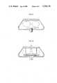
- FIG. 1shows in cross-section an edge portion of a semiconductor wafer having a coating which was previously spun onto the wafer
- FIG. 2illustrates in plan the direction of a jet of solvent onto the periphery of a semiconductor wafer in order to remove the peripheral coating, in accordance with an illustrative embodiment of the invention
- FIG. 3shows a side view of the process of FIG. 2
- FIG. 4shows the semiconductor wafer of FIG. 1 after the peripheral coating has been removed, in accordance with an illustrative embodiment of the invention
- FIG. 5is a schematic diagram showing the flow pattern of ambient within a typical spin-on coating apparatus
- FIG. 6is a schematic view of the flow pattern produced using the technique of the invention.
- FIG. 7is a schematic view of a spin-on coating apparatus designed in accordance with the principles of the invention.
- FIG. 1shows an edge portion of a semiconductor wafer 11 having a coating 12 which was spun onto the wafer.
- Edge bead region 13forms as a result of the spin application process.
- the coatingis thicker in edge bead region 13 than in interior region 14 where the coating has a substantially uniform thickness.
- coating 12can be photoresist.
- peripheral coating removal techniqueis applicable to any soluble coating.
- a jet of solventis directed at the periphery of a coated semiconductor wafer to selectively remove the peripheral edge bead region.
- semiconductor wafer 20is circular in shape and is spinning in the direction of arrow 21.
- the waferhas a diameter on the order of 50 mm to 125 mm and a thickness on the order of 20 mils.
- Pattern 22schematically illustrates the outline of the chip array which will subsequently be formed on the wafer.
- Nozzle 24is used to direct a jet of solvent 23 onto the wafer periphery.
- the jet of solventis applied a distance 28 inward from the edge of the wafer.
- Plume 25indicates the flow pattern of the solvent on the wafer surface and annular region 29 is the substantially coating free region on the surface of the wafer which results from the application of the jet of solvent.
- the jet of solventcan be aimed at the wafer periphery in a direction substantially the same as the direction of motion of the wafer. It should be noted, however, that other orientations of the jet of solvent with respect to the wafer motion, such as directing the jet opposite to the direction of motion of the wafer, can lead to satisfactory peripheral coating removal and are within the intended scope of the invention.
- the width of the coating-free peripheral region (29 of FIG. 2)can be altered by changing the distance (28 of FIG. 2) from the edge of wafer at which the jet is applied or by changing the direction of the jet with respect to the direction of motion of the wafer. This change in direction is indicated in FIG. 2 by the angle ⁇ which, illustratively, does not exceed approximately 15 degrees. If the jet of solvent is directed too sharply towards the edge of the wafer, the efficiency of removal of the edge coating is reduced. If the jet of solvent is directed too sharply towards the interior of the wafer, the solvent may tend to splash into the interior of the wafer and have a deleterious effect on interior portions of the coating.
- FIG. 3An alternate view of the application of the jet of solvent to the coated semiconductor wafer is shown in FIG. 3.
- Wafer 20is again shown spinning in the direction of arrow 21 and nozzle 24 is used to direct a jet of solvent 23 onto the wafer periphery.
- the nozzleforms an angle ⁇ with the plane of the wafer in the approximate range of 35 degrees to 45 degrees. However this does not exclude the use of angles down to 0 degrees.
- the nozzlehas an inner diameter of about 0.020 inches and the nozzle orifice is located approximately 0.5 cm above the plane of the wafer.
- the nozzleis machined with a smooth bore and polished surface around the orifice.
- a standard bellows(not shown) is included in the system to pull back the solvent in the nozzle at the end of the cycle. This insures a sharp turn on and turn off of the jet and prevents solvent dripping during other process steps.
- FIG. 4shows the wafer of FIG. 1 after the peripheral coating has been removed in accordance with the principles of the present invention.
- Common elements in FIGS. 1 and 4have the same identifying numerals.
- the portion 13 of coating 12 which has been removedis indicated by the broken curve and the portion 14 of coating 12 which remains is indicated by the solid curve.
- the boundary between the resist free periphery and the remaining resistis sharp as is indicate in FIG. 4.
- Photoresistis generally applied to a silicon wafer, which illustratively has a diameter of about 100 mm, using an automatic spin coater such as the GCA WafertracTM.
- a typical resist apply processinvolves the application of an adhesion promoter such as HMDS, which is spun to dryness, followed by the application of a standard resist, such as HPR 206, which is spun to final thickness at a high speed in the range of about 2000 rpm to 5000 rpm.
- the photoresistis spun almost dry before the use of the inventive peripheral coating removal technique.
- the waferis kept spinning after the resist is spun almost dry at a rate in the approximate range of 2000 rpm to 3000 rpm.
- a jet of solventsuch as AZ thinner, is directed at the periphery of the wafer for about 10 seconds.
- Approximately 6 cc of this solventapplied approximately 1/8 of an inch inward from the edge of the wafer, using the configuration of FIGS. 2 and 3, results in substantially complete removal of the photoresist from the beveled part of the silicon wafer was well as from a region approximately 1/8 to 3/16 inches back from the edge of the wafer.
- the jet of solventhas a velocity on the order of about 320 cm/second. After the jet is cut off, the wafer is allowed to spin for approximately 5 to 10 seconds to thoroughly dry.
- the plumewhich removes the resist in the desired manner from the periphery of the wafer.
- the density of solvent droplets, generated at the edge of the waferwill be acceptably low, assuming the following idealities: the wafers are perfectly flat; they are perfectly centered on the spin chuck; and the edges of the wafers are smooth and perfectly circular.
- the wafersare flat only to approximately 10 ⁇ m, so that as the wafer is spun, there is a vertical component of velocity at the periphery of the wafer which modulates the plume.
- the mechanical centering of the wafers on the chuckis only accurate to within approximately ⁇ 1/32 inch and the edges are not entirely smooth.
- the plumeis intercepted once each rotation by the presence of wafer flats, used to identify the material as to type and for orienting the wafers in processing equipment.
- any solvent droplets generated at the periphery of a waferwill tend to get caught up in the circular currents of FIG. 5 and can thereby reach the coated surface. Having landed on the photoresist surface, they locally disrupt the thin (approximately 1 ⁇ m) resist film and cause a defect after the photolithographic process. Such defects can be located anywhere within the wafer, but seem to be especially dense near the center.
- the solution to the problemis to break the closed circulation loops in a manner which will still yield satisfactory film thickness characteristics.
- the baffleinterrupts the circular air flow patterns which are responsible for the defects formed during the portion of the cycle that the peripheral photoresist removal technique is on, while allowing the externally imposed down-draft and natural currents to combine to form an ideal flow contour for the earlier portion of the cycle during which the resist is being spun to proper thickness.
- FIG. 7A diagram of the complete system is shown in FIG. 7. It has been found that the diameter of the baffle and its height above the wafer can be optimized.
- the optimum baffle diameterwhich has given the best protection and which is compatible with the spinner head geometry was found to be 3 inches outside diameter.
- the wall thicknesswas between 0.30 to 0.60 inches. This baffle diameter works well on both 100 mm and 125 mm diameter wafers.
- the corresponding optimum gapis 0.275 ⁇ 0.025 inch. If the gap is greater than 0.30 inch the baffle loses its effectiveness in controlling the droplet induced defect density.
- a gap smaller than 0.25 inchcauses the air velocity under the ring to increase to a point that the resist dries too fast there during the initial coating process, and the resist non-uniformity exceeds the permitted value ( ⁇ 1%).
- a third, and probably inter-related, variableis the air flow velocity associated with the down draft through the spinner head. This variable is determined by the flow rate through the exhaust tube (see FIG. 7) and has been formed to be optimum between 140 and 170 feet/minute, (assuming the nominal gap and baffle diameter values mentioned above). Flow rates above and below this nominal range will cause symptoms similar to the gap height being too low or too high.
Landscapes
- Physics & Mathematics (AREA)
- General Physics & Mathematics (AREA)
- Application Of Or Painting With Fluid Materials (AREA)
- Coating Apparatus (AREA)
- Exposure Of Semiconductors, Excluding Electron Or Ion Beam Exposure (AREA)
Abstract
Description
Claims (2)
Priority Applications (1)
| Application Number | Priority Date | Filing Date | Title |
|---|---|---|---|
| US06/535,916US4510176A (en) | 1983-09-26 | 1983-09-26 | Removal of coating from periphery of a semiconductor wafer |
Applications Claiming Priority (1)
| Application Number | Priority Date | Filing Date | Title |
|---|---|---|---|
| US06/535,916US4510176A (en) | 1983-09-26 | 1983-09-26 | Removal of coating from periphery of a semiconductor wafer |
Publications (1)
| Publication Number | Publication Date |
|---|---|
| US4510176Atrue US4510176A (en) | 1985-04-09 |
Family
ID=24136333
Family Applications (1)
| Application Number | Title | Priority Date | Filing Date |
|---|---|---|---|
| US06/535,916Expired - LifetimeUS4510176A (en) | 1983-09-26 | 1983-09-26 | Removal of coating from periphery of a semiconductor wafer |
Country Status (1)
| Country | Link |
|---|---|
| US (1) | US4510176A (en) |
Cited By (144)
| Publication number | Priority date | Publication date | Assignee | Title |
|---|---|---|---|---|
| US4732785A (en)* | 1986-09-26 | 1988-03-22 | Motorola, Inc. | Edge bead removal process for spin on films |
| US4741926A (en)* | 1985-10-29 | 1988-05-03 | Rca Corporation | Spin-coating procedure |
| US4790262A (en)* | 1985-10-07 | 1988-12-13 | Tokyo Denshi Kagaku Co., Ltd. | Thin-film coating apparatus |
| US4794021A (en)* | 1986-11-13 | 1988-12-27 | Microelectronics And Computer Technology Corporation | Method of providing a planarized polymer coating on a substrate wafer |
| US4800836A (en)* | 1987-03-27 | 1989-01-31 | Kabushiki Kaisha Toshiba | Resist coating apparatus |
| WO1989006378A1 (en)* | 1988-01-06 | 1989-07-13 | Olin Hunt Specialty Products Inc. | Use of particular mixtures of ethyl lactate and methyl ethyl ketone to remove undesirable peripheral material (e.g. edge beads) from photoresist-coated substrates |
| US4871417A (en)* | 1986-07-04 | 1989-10-03 | Dainippon Screen Mfg. Co., Ltd. | Method and apparatus for surface treating of substrates |
| US4886012A (en)* | 1987-06-30 | 1989-12-12 | Mitsubishi Denki Kabushiki Kaisha | Spin coating apparatus |
| US4895098A (en)* | 1988-02-04 | 1990-01-23 | Intelmatec Corporation | Lubricant applicator |
| US4899686A (en)* | 1988-04-08 | 1990-02-13 | Tokyo Electron Limited | Coating device |
| US5032430A (en)* | 1988-11-22 | 1991-07-16 | Nippon Leakless Industry Co., Ltd. | Method of producing a metal gasket |
| EP0469972A1 (en)* | 1990-08-01 | 1992-02-05 | Michel Balpe | Device for spreading a flowable paste, such as an edible paste on a horizontal surface, such as a cooking surface |
| US5116250A (en)* | 1987-09-18 | 1992-05-26 | Tokyo Ohka Kogyo Co., Ltd. | Method and apparatus for applying a coating material to a substrate |
| US5199988A (en)* | 1988-08-19 | 1993-04-06 | Hitachi Maxell, Ltd. | Manufacturing apparatus and method for recording medium |
| US5230743A (en)* | 1988-05-25 | 1993-07-27 | Semitool, Inc. | Method for single wafer processing in which a semiconductor wafer is contacted with a fluid |
| US5238713A (en)* | 1987-09-18 | 1993-08-24 | Tokyo Ohka Kogyo Co., Ltd. | Spin-on method and apparatus for applying coating material to a substrate, including an air flow developing and guiding step/means |
| US5238878A (en)* | 1992-02-18 | 1993-08-24 | Nec Corporation | Film forming method by spin coating in production of semiconductor device |
| US5279926A (en)* | 1992-05-06 | 1994-01-18 | International Business Machines Corporation | Method and apparatus for removing vapor from a pressurized sprayed liquid in the manufacture of semiconductor integrated circuits |
| US5362608A (en)* | 1992-08-24 | 1994-11-08 | Brewer Science, Inc. | Microlithographic substrate cleaning and compositions therefor |
| GB2277892A (en)* | 1993-05-13 | 1994-11-16 | Fujitsu Ltd | Apparatus for spin coating semiconductor wafers using solvent discharge prior to coating soln discharge |
| US5378511A (en)* | 1993-03-22 | 1995-01-03 | International Business Machines Corporation | Material-saving resist spinner and process |
| US5426073A (en)* | 1988-10-07 | 1995-06-20 | Fujitsu Limited | Method of fabricating semiconductor devices using an intermediate grinding step |
| US5449405A (en)* | 1991-10-29 | 1995-09-12 | International Business Machines Corporation | Material-saving resist spinner and process |
| WO1997006894A1 (en)* | 1995-08-21 | 1997-02-27 | Tapematic S.P.A. | Improved compact disc spin coater |
| US5670210A (en)* | 1994-10-27 | 1997-09-23 | Silicon Valley Group, Inc. | Method of uniformly coating a substrate |
| US5685908A (en)* | 1995-06-08 | 1997-11-11 | Essilor Of America, Inc. | Apparatus for spin coating a multifocal lens |
| US5688411A (en)* | 1995-03-09 | 1997-11-18 | Tokyo Ohka Kogyo Co., Ltd. | Method of and apparatus for removing coating from edge of substrate |
| US5705223A (en)* | 1994-07-26 | 1998-01-06 | International Business Machine Corp. | Method and apparatus for coating a semiconductor wafer |
| US5753301A (en)* | 1995-06-08 | 1998-05-19 | Essilor Of America, Inc. | Method for spin coating a multifocal lens |
| US5769945A (en)* | 1996-06-21 | 1998-06-23 | Micron Technology, Inc. | Spin coating bowl exhaust system |
| US5783097A (en)* | 1997-06-09 | 1998-07-21 | Taiwan Semiconductor Manufacturing Company, Ltd. | Process to avoid dielectric damage at the flat edge of the water |
| US5792259A (en)* | 1995-11-27 | 1998-08-11 | Dainippon Screen Mfg. Co., Ltd. | Substrate processing apparatus and air supply method in substrate processing apparatus |
| US5869211A (en)* | 1992-09-30 | 1999-02-09 | Hoya Corporation | Phase shift mask blank having a coated central shading pattern and uncoated peripheral portion |
| US5879577A (en)* | 1996-12-13 | 1999-03-09 | Taiwan Semiconductor Manufacturing Company Ltd. | Process for wafer peripheral edge defect reduction |
| US5911090A (en)* | 1994-09-16 | 1999-06-08 | Advanced Micro Devices, Inc. | Process and system for flattening secondary edgebeads on resist coated wafers |
| US5919520A (en)* | 1996-08-30 | 1999-07-06 | Tokyo Electron Limited | Coating method and apparatus for semiconductor process |
| US5952050A (en)* | 1996-02-27 | 1999-09-14 | Micron Technology, Inc. | Chemical dispensing system for semiconductor wafer processing |
| US5966628A (en)* | 1998-02-13 | 1999-10-12 | Taiwan Semiconductor Manufacturing Company, Ltd. | Process design for wafer edge in vlsi |
| US5965200A (en)* | 1994-08-03 | 1999-10-12 | Tokyo Electron Limited | Processing apparatus and processing method |
| US6001417A (en)* | 1996-09-18 | 1999-12-14 | Kabushiki Kaisha Toshiba | Resist coating method and resist coating apparatus |
| US6004631A (en)* | 1995-02-07 | 1999-12-21 | Seiko Epson Corporation | Apparatus and method of removing unnecessary matter and coating process using such method |
| US6037275A (en)* | 1998-08-27 | 2000-03-14 | Alliedsignal Inc. | Nanoporous silica via combined stream deposition |
| EP0881664A3 (en)* | 1997-05-23 | 2000-05-10 | SEZ Semiconductor-Equipment Zubehör für die Halbleiterfertigung AG | Treatment device for disk-like substrates, in particular silicon wafers |
| US6063232A (en)* | 1991-11-20 | 2000-05-16 | Enya Systems Limited | Method and apparatus for etching an edge face of a wafer |
| US6068881A (en)* | 1998-05-29 | 2000-05-30 | International Business Machines Corporation | Spin-apply tool having exhaust ring |
| US6114254A (en)* | 1996-10-15 | 2000-09-05 | Micron Technology, Inc. | Method for removing contaminants from a semiconductor wafer |
| US6113771A (en)* | 1998-04-21 | 2000-09-05 | Applied Materials, Inc. | Electro deposition chemistry |
| US6136163A (en)* | 1999-03-05 | 2000-10-24 | Applied Materials, Inc. | Apparatus for electro-chemical deposition with thermal anneal chamber |
| US6140254A (en)* | 1998-09-18 | 2000-10-31 | Alliedsignal Inc. | Edge bead removal for nanoporous dielectric silica coatings |
| US6153361A (en)* | 1999-01-19 | 2000-11-28 | United Microelectronics Corp | Method of removing photoresist at the edge of wafers |
| US6217936B1 (en)* | 1999-02-26 | 2001-04-17 | Advanced Micro Devices | Semiconductor fabrication extended particle collection cup |
| US6228233B1 (en) | 1998-11-30 | 2001-05-08 | Applied Materials, Inc. | Inflatable compliant bladder assembly |
| US6254760B1 (en) | 1999-03-05 | 2001-07-03 | Applied Materials, Inc. | Electro-chemical deposition system and method |
| US6258220B1 (en) | 1998-11-30 | 2001-07-10 | Applied Materials, Inc. | Electro-chemical deposition system |
| US6261433B1 (en) | 1998-04-21 | 2001-07-17 | Applied Materials, Inc. | Electro-chemical deposition system and method of electroplating on substrates |
| US6267853B1 (en) | 1999-07-09 | 2001-07-31 | Applied Materials, Inc. | Electro-chemical deposition system |
| US6290865B1 (en) | 1998-11-30 | 2001-09-18 | Applied Materials, Inc. | Spin-rinse-drying process for electroplated semiconductor wafers |
| US20010037858A1 (en)* | 2000-05-08 | 2001-11-08 | Hiroki Taniyama | Processing apparatus, processing system and processing method |
| US20020004100A1 (en)* | 1994-10-27 | 2002-01-10 | Emir Gurer | Method of uniformly coating a substrate |
| US20020037641A1 (en)* | 1998-06-01 | 2002-03-28 | Ritzdorf Thomas L. | Method and apparatus for low temperature annealing of metallization micro-structure in the production of a microelectronic device |
| US20020040679A1 (en)* | 1990-05-18 | 2002-04-11 | Reardon Timothy J. | Semiconductor processing apparatus |
| US6379522B1 (en) | 1999-01-11 | 2002-04-30 | Applied Materials, Inc. | Electrodeposition chemistry for filling of apertures with reflective metal |
| US6395086B1 (en)* | 1993-04-08 | 2002-05-28 | Chartered Semiconductor Manufacturing Pte Ltd | Shield for wafer station |
| US20020074233A1 (en)* | 1998-02-04 | 2002-06-20 | Semitool, Inc. | Method and apparatus for low temperature annealing of metallization micro-structures in the production of a microelectronic device |
| US6417117B1 (en) | 1996-06-21 | 2002-07-09 | Micron Technology, Inc. | Spin coating spindle and chuck assembly |
| US6416647B1 (en) | 1998-04-21 | 2002-07-09 | Applied Materials, Inc. | Electro-chemical deposition cell for face-up processing of single semiconductor substrates |
| AT409348B (en)* | 1999-04-22 | 2002-07-25 | Thallner Erich | DEVICE FOR APPLYING MATERIALS TO SUBSTRATES, ESPECIALLY FOR PAINTING SI WAFERS |
| US20020113039A1 (en)* | 1999-07-09 | 2002-08-22 | Mok Yeuk-Fai Edwin | Integrated semiconductor substrate bevel cleaning apparatus and method |
| US20020112964A1 (en)* | 2000-07-12 | 2002-08-22 | Applied Materials, Inc. | Process window for gap-fill on very high aspect ratio structures using additives in low acid copper baths |
| US20020144973A1 (en)* | 1999-01-22 | 2002-10-10 | Semitool, Inc. | Selective treatment of the surface of a microelectronic workpiece |
| US6478937B2 (en) | 2001-01-19 | 2002-11-12 | Applied Material, Inc. | Substrate holder system with substrate extension apparatus and associated method |
| KR100365042B1 (en)* | 1998-11-30 | 2002-12-16 | 다이닛뽕스크린 세이조오 가부시키가이샤 | Coating solution applying method and apparatus |
| US6494221B1 (en)* | 1998-11-27 | 2002-12-17 | Sez Ag | Device for wet etching an edge of a semiconductor disk |
| US6497784B1 (en)* | 1998-02-11 | 2002-12-24 | International Business Machines Corporation | Semiconductor wafer edge bead removal method and tool |
| US20030023402A1 (en)* | 2000-11-16 | 2003-01-30 | Makoto Kobayashi | Wafer shape evaluating method and device producing method, wafer and wafer selecting method |
| US20030021893A1 (en)* | 2001-06-15 | 2003-01-30 | Fuji Photo Film Co., Ltd. | Method for producing optical information recording medium |
| US6516815B1 (en)* | 1999-07-09 | 2003-02-11 | Applied Materials, Inc. | Edge bead removal/spin rinse dry (EBR/SRD) module |
| US20030054616A1 (en)* | 2001-08-29 | 2003-03-20 | Honeywell International Inc. | Electronic devices and methods of manufacture |
| US20030062599A1 (en)* | 2001-09-21 | 2003-04-03 | Catalysts & Chemicals Industries Co., Ltd. | Process for producing semiconductor substrates and semiconductor substrates |
| US6544399B1 (en) | 1999-01-11 | 2003-04-08 | Applied Materials, Inc. | Electrodeposition chemistry for filling apertures with reflective metal |
| US6551484B2 (en) | 1999-04-08 | 2003-04-22 | Applied Materials, Inc. | Reverse voltage bias for electro-chemical plating system and method |
| US6551488B1 (en) | 1999-04-08 | 2003-04-22 | Applied Materials, Inc. | Segmenting of processing system into wet and dry areas |
| US6557237B1 (en) | 1999-04-08 | 2003-05-06 | Applied Materials, Inc. | Removable modular cell for electro-chemical plating and method |
| US6565920B1 (en)* | 2000-06-08 | 2003-05-20 | Honeywell International Inc. | Edge bead removal for spin-on materials containing low volatility solvents fusing carbon dioxide cleaning |
| US6571657B1 (en) | 1999-04-08 | 2003-06-03 | Applied Materials Inc. | Multiple blade robot adjustment apparatus and associated method |
| US6576110B2 (en) | 2000-07-07 | 2003-06-10 | Applied Materials, Inc. | Coated anode apparatus and associated method |
| US6582578B1 (en) | 1999-04-08 | 2003-06-24 | Applied Materials, Inc. | Method and associated apparatus for tilting a substrate upon entry for metal deposition |
| US6585876B2 (en) | 1999-04-08 | 2003-07-01 | Applied Materials Inc. | Flow diffuser to be used in electro-chemical plating system and method |
| US20030141018A1 (en)* | 2002-01-28 | 2003-07-31 | Applied Materials, Inc. | Electroless deposition apparatus |
| US20030146102A1 (en)* | 2002-02-05 | 2003-08-07 | Applied Materials, Inc. | Method for forming copper interconnects |
| US6610189B2 (en) | 2001-01-03 | 2003-08-26 | Applied Materials, Inc. | Method and associated apparatus to mechanically enhance the deposition of a metal film within a feature |
| US6615854B1 (en)* | 1999-05-19 | 2003-09-09 | Ebara Corporation | Wafer cleaning apparatus |
| US20030201166A1 (en)* | 2002-04-29 | 2003-10-30 | Applied Materials, Inc. | method for regulating the electrical power applied to a substrate during an immersion process |
| US20030201185A1 (en)* | 2002-04-29 | 2003-10-30 | Applied Materials, Inc. | In-situ pre-clean for electroplating process |
| US20030203650A1 (en)* | 2002-04-26 | 2003-10-30 | Robbins Michael D. | Method and apparatus for shaping thin films in the near-edge regions of in-process semiconductor substrates |
| US20030209443A1 (en)* | 2002-05-09 | 2003-11-13 | Applied Materials, Inc. | Substrate support with fluid retention band |
| US6662673B1 (en) | 1999-04-08 | 2003-12-16 | Applied Materials, Inc. | Linear motion apparatus and associated method |
| US20040003873A1 (en)* | 1999-03-05 | 2004-01-08 | Applied Materials, Inc. | Method and apparatus for annealing copper films |
| US20040023494A1 (en)* | 1998-03-13 | 2004-02-05 | Semitool, Inc. | Selective treatment of microelectronic workpiece surfaces |
| US6708701B2 (en)* | 2001-10-16 | 2004-03-23 | Applied Materials Inc. | Capillary ring |
| US20040079633A1 (en)* | 2000-07-05 | 2004-04-29 | Applied Materials, Inc. | Apparatus for electro chemical deposition of copper metallization with the capability of in-situ thermal annealing |
| US6742279B2 (en) | 2002-01-16 | 2004-06-01 | Applied Materials Inc. | Apparatus and method for rinsing substrates |
| US20040140203A1 (en)* | 2003-01-21 | 2004-07-22 | Applied Materials,Inc. | Liquid isolation of contact rings |
| US6770565B2 (en) | 2002-01-08 | 2004-08-03 | Applied Materials Inc. | System for planarizing metal conductive layers |
| US20040149573A1 (en)* | 2003-01-31 | 2004-08-05 | Applied Materials, Inc. | Contact ring with embedded flexible contacts |
| US20040154185A1 (en)* | 1997-07-10 | 2004-08-12 | Applied Materials, Inc. | Method and apparatus for heating and cooling substrates |
| US6786996B2 (en) | 2001-10-16 | 2004-09-07 | Applied Materials Inc. | Apparatus and method for edge bead removal |
| US6806186B2 (en) | 1998-02-04 | 2004-10-19 | Semitool, Inc. | Submicron metallization using electrochemical deposition |
| US20040206373A1 (en)* | 2003-04-18 | 2004-10-21 | Applied Materials, Inc. | Spin rinse dry cell |
| US20040206628A1 (en)* | 2003-04-18 | 2004-10-21 | Applied Materials, Inc. | Electrical bias during wafer exit from electrolyte bath |
| US20040209414A1 (en)* | 2003-04-18 | 2004-10-21 | Applied Materials, Inc. | Two position anneal chamber |
| US6808612B2 (en) | 2000-05-23 | 2004-10-26 | Applied Materials, Inc. | Method and apparatus to overcome anomalies in copper seed layers and to tune for feature size and aspect ratio |
| US20040215418A1 (en)* | 2001-09-14 | 2004-10-28 | Makoto Kobayashi | Wafer shape evaluating method, wafer, and wafer selecting method |
| US6824612B2 (en) | 2001-12-26 | 2004-11-30 | Applied Materials, Inc. | Electroless plating system |
| US6837978B1 (en) | 1999-04-08 | 2005-01-04 | Applied Materials, Inc. | Deposition uniformity control for electroplating apparatus, and associated method |
| US20050032391A1 (en)* | 1998-03-13 | 2005-02-10 | Semitool, Inc. | Method for processing a semiconductor wafer |
| US20050042879A1 (en)* | 2003-08-22 | 2005-02-24 | Zhiping Yin | Masking methods |
| US20050092602A1 (en)* | 2003-10-29 | 2005-05-05 | Harald Herchen | Electrochemical plating cell having a membrane stack |
| US20050092601A1 (en)* | 2003-10-29 | 2005-05-05 | Harald Herchen | Electrochemical plating cell having a diffusion member |
| US6913680B1 (en) | 2000-05-02 | 2005-07-05 | Applied Materials, Inc. | Method of application of electrical biasing to enhance metal deposition |
| US20050217707A1 (en)* | 1998-03-13 | 2005-10-06 | Aegerter Brian K | Selective processing of microelectronic workpiece surfaces |
| US20050218000A1 (en)* | 2004-04-06 | 2005-10-06 | Applied Materials, Inc. | Conditioning of contact leads for metal plating systems |
| US20050255702A1 (en)* | 2004-05-17 | 2005-11-17 | Honeycutt Jeffrey W | Methods of processing a semiconductor substrate |
| US20050284754A1 (en)* | 2004-06-24 | 2005-12-29 | Harald Herchen | Electric field reducing thrust plate |
| US7018943B2 (en) | 1994-10-27 | 2006-03-28 | Asml Holding N.V. | Method of uniformly coating a substrate |
| US7025861B2 (en) | 2003-02-06 | 2006-04-11 | Applied Materials | Contact plating apparatus |
| US7030039B2 (en) | 1994-10-27 | 2006-04-18 | Asml Holding N.V. | Method of uniformly coating a substrate |
| US20060099131A1 (en)* | 2004-11-03 | 2006-05-11 | Kellogg Brown And Root, Inc. | Maximum reaction rate converter system for exothermic reactions |
| US20060102467A1 (en)* | 2004-11-15 | 2006-05-18 | Harald Herchen | Current collimation for thin seed and direct plating |
| US20060141809A1 (en)* | 2004-03-12 | 2006-06-29 | Semitool, Inc. | Single side workpiece processing |
| US20060137213A1 (en)* | 2004-12-24 | 2006-06-29 | Seiko Epson Corporation | Solvent removal apparatus and method |
| US20060150432A1 (en)* | 2005-01-11 | 2006-07-13 | Pham Xuyen N | Multi-zone shower head for drying single semiconductor substrate |
| US20060175201A1 (en)* | 2005-02-07 | 2006-08-10 | Hooman Hafezi | Immersion process for electroplating applications |
| US20070014958A1 (en)* | 2005-07-08 | 2007-01-18 | Chaplin Ernest R | Hanger labels, label assemblies and methods for forming the same |
| US20070110895A1 (en)* | 2005-03-08 | 2007-05-17 | Jason Rye | Single side workpiece processing |
| US20070137679A1 (en)* | 2004-03-12 | 2007-06-21 | Rye Jason A | Single side workpiece processing |
| US20070254463A1 (en)* | 2006-04-28 | 2007-11-01 | Takayo Kobayashi | Semiconductor device and method of manufacturing the same |
| US20080011334A1 (en)* | 2006-02-22 | 2008-01-17 | Rye Jason A | Single side workpiece processing |
| US20080017613A1 (en)* | 2004-07-09 | 2008-01-24 | Sekisui Chemical Co., Ltd. | Method for processing outer periphery of substrate and apparatus thereof |
| US7354631B2 (en) | 2003-11-06 | 2008-04-08 | Micron Technology, Inc. | Chemical vapor deposition apparatus and methods |
| US7691559B2 (en) | 2005-06-30 | 2010-04-06 | Taiwan Semiconductor Manufacturing Company, Ltd. | Immersion lithography edge bead removal |
| US20100178472A1 (en)* | 2006-08-14 | 2010-07-15 | Meynen Herman C G D C | Method of Preparing A Patterned Film With A Developing Solvent |
| CN101339366B (en)* | 2007-07-05 | 2011-09-07 | Asml荷兰有限公司 | Substrate processing method and device manufacture method |
| US20120276753A1 (en)* | 2011-04-26 | 2012-11-01 | Tokyo Electron Limited | Coating treatment apparatus, coating and developing treatment system, coating treatment method, and non-transitory recording medium having program recorded thereon for executing coating treatment method |
Citations (3)
| Publication number | Priority date | Publication date | Assignee | Title |
|---|---|---|---|---|
| JPS5217813A (en)* | 1975-07-29 | 1977-02-10 | Fuji Photo Film Co Ltd | Photographic light sensitive material and method of spin coating to provide the same |
| US4113492A (en)* | 1976-04-08 | 1978-09-12 | Fuji Photo Film Co., Ltd. | Spin coating process |
| US4393807A (en)* | 1979-09-19 | 1983-07-19 | Fujitsu Limited | Spinner |
- 1983
- 1983-09-26USUS06/535,916patent/US4510176A/ennot_activeExpired - Lifetime
Patent Citations (3)
| Publication number | Priority date | Publication date | Assignee | Title |
|---|---|---|---|---|
| JPS5217813A (en)* | 1975-07-29 | 1977-02-10 | Fuji Photo Film Co Ltd | Photographic light sensitive material and method of spin coating to provide the same |
| US4113492A (en)* | 1976-04-08 | 1978-09-12 | Fuji Photo Film Co., Ltd. | Spin coating process |
| US4393807A (en)* | 1979-09-19 | 1983-07-19 | Fujitsu Limited | Spinner |
Cited By (221)
| Publication number | Priority date | Publication date | Assignee | Title |
|---|---|---|---|---|
| US4790262A (en)* | 1985-10-07 | 1988-12-13 | Tokyo Denshi Kagaku Co., Ltd. | Thin-film coating apparatus |
| US4741926A (en)* | 1985-10-29 | 1988-05-03 | Rca Corporation | Spin-coating procedure |
| US4871417A (en)* | 1986-07-04 | 1989-10-03 | Dainippon Screen Mfg. Co., Ltd. | Method and apparatus for surface treating of substrates |
| US4732785A (en)* | 1986-09-26 | 1988-03-22 | Motorola, Inc. | Edge bead removal process for spin on films |
| US4794021A (en)* | 1986-11-13 | 1988-12-27 | Microelectronics And Computer Technology Corporation | Method of providing a planarized polymer coating on a substrate wafer |
| US4800836A (en)* | 1987-03-27 | 1989-01-31 | Kabushiki Kaisha Toshiba | Resist coating apparatus |
| US4886012A (en)* | 1987-06-30 | 1989-12-12 | Mitsubishi Denki Kabushiki Kaisha | Spin coating apparatus |
| US5238713A (en)* | 1987-09-18 | 1993-08-24 | Tokyo Ohka Kogyo Co., Ltd. | Spin-on method and apparatus for applying coating material to a substrate, including an air flow developing and guiding step/means |
| US5116250A (en)* | 1987-09-18 | 1992-05-26 | Tokyo Ohka Kogyo Co., Ltd. | Method and apparatus for applying a coating material to a substrate |
| WO1989006378A1 (en)* | 1988-01-06 | 1989-07-13 | Olin Hunt Specialty Products Inc. | Use of particular mixtures of ethyl lactate and methyl ethyl ketone to remove undesirable peripheral material (e.g. edge beads) from photoresist-coated substrates |
| US4886728A (en)* | 1988-01-06 | 1989-12-12 | Olin Hunt Specialty Products Inc. | Use of particular mixtures of ethyl lactate and methyl ethyl ketone to remove undesirable peripheral material (e.g. edge beads) from photoresist-coated substrates |
| US4895098A (en)* | 1988-02-04 | 1990-01-23 | Intelmatec Corporation | Lubricant applicator |
| US4899686A (en)* | 1988-04-08 | 1990-02-13 | Tokyo Electron Limited | Coating device |
| US5230743A (en)* | 1988-05-25 | 1993-07-27 | Semitool, Inc. | Method for single wafer processing in which a semiconductor wafer is contacted with a fluid |
| US5199988A (en)* | 1988-08-19 | 1993-04-06 | Hitachi Maxell, Ltd. | Manufacturing apparatus and method for recording medium |
| US5426073A (en)* | 1988-10-07 | 1995-06-20 | Fujitsu Limited | Method of fabricating semiconductor devices using an intermediate grinding step |
| US5032430A (en)* | 1988-11-22 | 1991-07-16 | Nippon Leakless Industry Co., Ltd. | Method of producing a metal gasket |
| US7138016B2 (en) | 1990-05-18 | 2006-11-21 | Semitool, Inc. | Semiconductor processing apparatus |
| US7094291B2 (en) | 1990-05-18 | 2006-08-22 | Semitool, Inc. | Semiconductor processing apparatus |
| US20020040679A1 (en)* | 1990-05-18 | 2002-04-11 | Reardon Timothy J. | Semiconductor processing apparatus |
| EP0469972A1 (en)* | 1990-08-01 | 1992-02-05 | Michel Balpe | Device for spreading a flowable paste, such as an edible paste on a horizontal surface, such as a cooking surface |
| FR2665381A1 (en)* | 1990-08-01 | 1992-02-07 | Balpe Michel | DEVICE FOR SPREADING A BLENDED PASTE, SUCH AS A RAW FOOD PASTE, ON A HORIZONTAL SIDE, SUCH AS A COOKING SIDE. |
| US5449405A (en)* | 1991-10-29 | 1995-09-12 | International Business Machines Corporation | Material-saving resist spinner and process |
| US6063232A (en)* | 1991-11-20 | 2000-05-16 | Enya Systems Limited | Method and apparatus for etching an edge face of a wafer |
| US5238878A (en)* | 1992-02-18 | 1993-08-24 | Nec Corporation | Film forming method by spin coating in production of semiconductor device |
| US5279926A (en)* | 1992-05-06 | 1994-01-18 | International Business Machines Corporation | Method and apparatus for removing vapor from a pressurized sprayed liquid in the manufacture of semiconductor integrated circuits |
| US5362608A (en)* | 1992-08-24 | 1994-11-08 | Brewer Science, Inc. | Microlithographic substrate cleaning and compositions therefor |
| US5869211A (en)* | 1992-09-30 | 1999-02-09 | Hoya Corporation | Phase shift mask blank having a coated central shading pattern and uncoated peripheral portion |
| US5378511A (en)* | 1993-03-22 | 1995-01-03 | International Business Machines Corporation | Material-saving resist spinner and process |
| US6395086B1 (en)* | 1993-04-08 | 2002-05-28 | Chartered Semiconductor Manufacturing Pte Ltd | Shield for wafer station |
| GB2277892B (en)* | 1993-05-13 | 1997-08-20 | Fujitsu Ltd | Method and apparatus for spin coating and a method for manufacturing a semiconductor device |
| GB2277892A (en)* | 1993-05-13 | 1994-11-16 | Fujitsu Ltd | Apparatus for spin coating semiconductor wafers using solvent discharge prior to coating soln discharge |
| US6033728A (en)* | 1993-05-13 | 2000-03-07 | Fujitsu Limited | Apparatus for spin coating, a method for spin coating and a method for manufacturing semiconductor device |
| US5705223A (en)* | 1994-07-26 | 1998-01-06 | International Business Machine Corp. | Method and apparatus for coating a semiconductor wafer |
| US5965200A (en)* | 1994-08-03 | 1999-10-12 | Tokyo Electron Limited | Processing apparatus and processing method |
| US5911090A (en)* | 1994-09-16 | 1999-06-08 | Advanced Micro Devices, Inc. | Process and system for flattening secondary edgebeads on resist coated wafers |
| US5670210A (en)* | 1994-10-27 | 1997-09-23 | Silicon Valley Group, Inc. | Method of uniformly coating a substrate |
| US7030039B2 (en) | 1994-10-27 | 2006-04-18 | Asml Holding N.V. | Method of uniformly coating a substrate |
| US7018943B2 (en) | 1994-10-27 | 2006-03-28 | Asml Holding N.V. | Method of uniformly coating a substrate |
| US6977098B2 (en) | 1994-10-27 | 2005-12-20 | Asml Holding N.V. | Method of uniformly coating a substrate |
| US20020004100A1 (en)* | 1994-10-27 | 2002-01-10 | Emir Gurer | Method of uniformly coating a substrate |
| US6004631A (en)* | 1995-02-07 | 1999-12-21 | Seiko Epson Corporation | Apparatus and method of removing unnecessary matter and coating process using such method |
| US5688411A (en)* | 1995-03-09 | 1997-11-18 | Tokyo Ohka Kogyo Co., Ltd. | Method of and apparatus for removing coating from edge of substrate |
| US5753301A (en)* | 1995-06-08 | 1998-05-19 | Essilor Of America, Inc. | Method for spin coating a multifocal lens |
| US5685908A (en)* | 1995-06-08 | 1997-11-11 | Essilor Of America, Inc. | Apparatus for spin coating a multifocal lens |
| WO1997006894A1 (en)* | 1995-08-21 | 1997-02-27 | Tapematic S.P.A. | Improved compact disc spin coater |
| US5803968A (en)* | 1995-08-21 | 1998-09-08 | Schwartz; Vladimir | Compact disc spin coater |
| US5792259A (en)* | 1995-11-27 | 1998-08-11 | Dainippon Screen Mfg. Co., Ltd. | Substrate processing apparatus and air supply method in substrate processing apparatus |
| US6793764B1 (en) | 1996-02-27 | 2004-09-21 | Micron Technology, Inc. | Chemical dispensing system for semiconductor wafer processing |
| US7470344B1 (en) | 1996-02-27 | 2008-12-30 | Micron Technology, Inc. | Chemical dispensing system for semiconductor wafer processing |
| US5952050A (en)* | 1996-02-27 | 1999-09-14 | Micron Technology, Inc. | Chemical dispensing system for semiconductor wafer processing |
| US6417117B1 (en) | 1996-06-21 | 2002-07-09 | Micron Technology, Inc. | Spin coating spindle and chuck assembly |
| US6599571B2 (en) | 1996-06-21 | 2003-07-29 | Micron Technology, Inc. | Spin coating methods |
| US6132802A (en)* | 1996-06-21 | 2000-10-17 | Micron Technology, Inc. | Methods for exhausting a wafer coating apparatus |
| US5769945A (en)* | 1996-06-21 | 1998-06-23 | Micron Technology, Inc. | Spin coating bowl exhaust system |
| US6511540B1 (en) | 1996-06-21 | 2003-01-28 | Micron Technology, Inc. | Spin coating spindle and chuck assembly |
| US6162294A (en)* | 1996-06-21 | 2000-12-19 | Micron Technology, Inc. | Spin coating bowl exhaust system |
| US6221157B1 (en)* | 1996-06-21 | 2001-04-24 | Micron Technology, Inc. | Spin coating bowl exhaust system |
| US6749688B2 (en) | 1996-08-30 | 2004-06-15 | Tokyo Electron Limited | Coating method and apparatus for semiconductor process |
| US5919520A (en)* | 1996-08-30 | 1999-07-06 | Tokyo Electron Limited | Coating method and apparatus for semiconductor process |
| US6001417A (en)* | 1996-09-18 | 1999-12-14 | Kabushiki Kaisha Toshiba | Resist coating method and resist coating apparatus |
| US6506689B2 (en) | 1996-10-15 | 2003-01-14 | Micron Technology, Inc. | Method for removing contaminants from a semiconductor wafer |
| US6114254A (en)* | 1996-10-15 | 2000-09-05 | Micron Technology, Inc. | Method for removing contaminants from a semiconductor wafer |
| US6255228B1 (en) | 1996-10-15 | 2001-07-03 | Micron Technology, Inc. | Method for removing contaminants from a semiconductor wafer |
| US5879577A (en)* | 1996-12-13 | 1999-03-09 | Taiwan Semiconductor Manufacturing Company Ltd. | Process for wafer peripheral edge defect reduction |
| EP0881664A3 (en)* | 1997-05-23 | 2000-05-10 | SEZ Semiconductor-Equipment Zubehör für die Halbleiterfertigung AG | Treatment device for disk-like substrates, in particular silicon wafers |
| US5783097A (en)* | 1997-06-09 | 1998-07-21 | Taiwan Semiconductor Manufacturing Company, Ltd. | Process to avoid dielectric damage at the flat edge of the water |
| US6929774B2 (en) | 1997-07-10 | 2005-08-16 | Applied Materials, Inc. | Method and apparatus for heating and cooling substrates |
| US20040154185A1 (en)* | 1997-07-10 | 2004-08-12 | Applied Materials, Inc. | Method and apparatus for heating and cooling substrates |
| US7144805B2 (en) | 1998-02-04 | 2006-12-05 | Semitool, Inc. | Method of submicron metallization using electrochemical deposition of recesses including a first deposition at a first current density and a second deposition at an increased current density |
| US20050051436A1 (en)* | 1998-02-04 | 2005-03-10 | Semitool, Inc. | Method of submicron metallization using electrochemical deposition of recesses including a first deposition at a first current density and a second deposition at an increased current density |
| US20060208272A1 (en)* | 1998-02-04 | 2006-09-21 | Semitool, Inc. | Method for filling recessed micro-structures with metallization in the production of a microelectronic device |
| US6806186B2 (en) | 1998-02-04 | 2004-10-19 | Semitool, Inc. | Submicron metallization using electrochemical deposition |
| US7462269B2 (en) | 1998-02-04 | 2008-12-09 | Semitool, Inc. | Method for low temperature annealing of metallization micro-structures in the production of a microelectronic device |
| US20020074233A1 (en)* | 1998-02-04 | 2002-06-20 | Semitool, Inc. | Method and apparatus for low temperature annealing of metallization micro-structures in the production of a microelectronic device |
| US6508920B1 (en) | 1998-02-04 | 2003-01-21 | Semitool, Inc. | Apparatus for low-temperature annealing of metallization microstructures in the production of a microelectronic device |
| US6497784B1 (en)* | 1998-02-11 | 2002-12-24 | International Business Machines Corporation | Semiconductor wafer edge bead removal method and tool |
| US6114747A (en)* | 1998-02-13 | 2000-09-05 | Taiwan Semiconductor Manufacturing Company | Process design for wafer edge in VLSI |
| US5966628A (en)* | 1998-02-13 | 1999-10-12 | Taiwan Semiconductor Manufacturing Company, Ltd. | Process design for wafer edge in vlsi |
| US20040023494A1 (en)* | 1998-03-13 | 2004-02-05 | Semitool, Inc. | Selective treatment of microelectronic workpiece surfaces |
| US20050233589A1 (en)* | 1998-03-13 | 2005-10-20 | Aegerter Brian K | Processes for removing residue from a workpiece |
| US20050032391A1 (en)* | 1998-03-13 | 2005-02-10 | Semitool, Inc. | Method for processing a semiconductor wafer |
| US7399713B2 (en) | 1998-03-13 | 2008-07-15 | Semitool, Inc. | Selective treatment of microelectric workpiece surfaces |
| US20050217707A1 (en)* | 1998-03-13 | 2005-10-06 | Aegerter Brian K | Selective processing of microelectronic workpiece surfaces |
| US6350366B1 (en) | 1998-04-21 | 2002-02-26 | Applied Materials, Inc. | Electro deposition chemistry |
| US6113771A (en)* | 1998-04-21 | 2000-09-05 | Applied Materials, Inc. | Electro deposition chemistry |
| US6416647B1 (en) | 1998-04-21 | 2002-07-09 | Applied Materials, Inc. | Electro-chemical deposition cell for face-up processing of single semiconductor substrates |
| US20030205474A1 (en)* | 1998-04-21 | 2003-11-06 | Applied Materials, Inc. | Electro deposition chemistry |
| USRE40218E1 (en)* | 1998-04-21 | 2008-04-08 | Uziel Landau | Electro-chemical deposition system and method of electroplating on substrates |
| US6261433B1 (en) | 1998-04-21 | 2001-07-17 | Applied Materials, Inc. | Electro-chemical deposition system and method of electroplating on substrates |
| US6610191B2 (en) | 1998-04-21 | 2003-08-26 | Applied Materials, Inc. | Electro deposition chemistry |
| US6068881A (en)* | 1998-05-29 | 2000-05-30 | International Business Machines Corporation | Spin-apply tool having exhaust ring |
| US6994776B2 (en)* | 1998-06-01 | 2006-02-07 | Semitool Inc. | Method and apparatus for low temperature annealing of metallization micro-structure in the production of a microelectronic device |
| US20020037641A1 (en)* | 1998-06-01 | 2002-03-28 | Ritzdorf Thomas L. | Method and apparatus for low temperature annealing of metallization micro-structure in the production of a microelectronic device |
| US6037275A (en)* | 1998-08-27 | 2000-03-14 | Alliedsignal Inc. | Nanoporous silica via combined stream deposition |
| US6140254A (en)* | 1998-09-18 | 2000-10-31 | Alliedsignal Inc. | Edge bead removal for nanoporous dielectric silica coatings |
| US6494221B1 (en)* | 1998-11-27 | 2002-12-17 | Sez Ag | Device for wet etching an edge of a semiconductor disk |
| KR100365042B1 (en)* | 1998-11-30 | 2002-12-16 | 다이닛뽕스크린 세이조오 가부시키가이샤 | Coating solution applying method and apparatus |
| US6228233B1 (en) | 1998-11-30 | 2001-05-08 | Applied Materials, Inc. | Inflatable compliant bladder assembly |
| US6290865B1 (en) | 1998-11-30 | 2001-09-18 | Applied Materials, Inc. | Spin-rinse-drying process for electroplated semiconductor wafers |
| US6635157B2 (en) | 1998-11-30 | 2003-10-21 | Applied Materials, Inc. | Electro-chemical deposition system |
| US6258220B1 (en) | 1998-11-30 | 2001-07-10 | Applied Materials, Inc. | Electro-chemical deposition system |
| US6544399B1 (en) | 1999-01-11 | 2003-04-08 | Applied Materials, Inc. | Electrodeposition chemistry for filling apertures with reflective metal |
| US6379522B1 (en) | 1999-01-11 | 2002-04-30 | Applied Materials, Inc. | Electrodeposition chemistry for filling of apertures with reflective metal |
| US6596151B2 (en) | 1999-01-11 | 2003-07-22 | Applied Materials, Inc. | Electrodeposition chemistry for filling of apertures with reflective metal |
| US6153361A (en)* | 1999-01-19 | 2000-11-28 | United Microelectronics Corp | Method of removing photoresist at the edge of wafers |
| US20020144973A1 (en)* | 1999-01-22 | 2002-10-10 | Semitool, Inc. | Selective treatment of the surface of a microelectronic workpiece |
| US20020168863A1 (en)* | 1999-01-27 | 2002-11-14 | Semitool, Inc. | Selective treatment of the surface of a microelectronic workpiece |
| US6217936B1 (en)* | 1999-02-26 | 2001-04-17 | Advanced Micro Devices | Semiconductor fabrication extended particle collection cup |
| US6254760B1 (en) | 1999-03-05 | 2001-07-03 | Applied Materials, Inc. | Electro-chemical deposition system and method |
| US6136163A (en)* | 1999-03-05 | 2000-10-24 | Applied Materials, Inc. | Apparatus for electro-chemical deposition with thermal anneal chamber |
| US20040003873A1 (en)* | 1999-03-05 | 2004-01-08 | Applied Materials, Inc. | Method and apparatus for annealing copper films |
| US7192494B2 (en) | 1999-03-05 | 2007-03-20 | Applied Materials, Inc. | Method and apparatus for annealing copper films |
| US6585876B2 (en) | 1999-04-08 | 2003-07-01 | Applied Materials Inc. | Flow diffuser to be used in electro-chemical plating system and method |
| US20030168346A1 (en)* | 1999-04-08 | 2003-09-11 | Applied Materials, Inc. | Segmenting of processing system into wet and dry areas |
| US6582578B1 (en) | 1999-04-08 | 2003-06-24 | Applied Materials, Inc. | Method and associated apparatus for tilting a substrate upon entry for metal deposition |
| US6837978B1 (en) | 1999-04-08 | 2005-01-04 | Applied Materials, Inc. | Deposition uniformity control for electroplating apparatus, and associated method |
| US6571657B1 (en) | 1999-04-08 | 2003-06-03 | Applied Materials Inc. | Multiple blade robot adjustment apparatus and associated method |
| US6551484B2 (en) | 1999-04-08 | 2003-04-22 | Applied Materials, Inc. | Reverse voltage bias for electro-chemical plating system and method |
| US6551488B1 (en) | 1999-04-08 | 2003-04-22 | Applied Materials, Inc. | Segmenting of processing system into wet and dry areas |
| US6557237B1 (en) | 1999-04-08 | 2003-05-06 | Applied Materials, Inc. | Removable modular cell for electro-chemical plating and method |
| US6662673B1 (en) | 1999-04-08 | 2003-12-16 | Applied Materials, Inc. | Linear motion apparatus and associated method |
| AT409348B (en)* | 1999-04-22 | 2002-07-25 | Thallner Erich | DEVICE FOR APPLYING MATERIALS TO SUBSTRATES, ESPECIALLY FOR PAINTING SI WAFERS |
| US6485568B1 (en) | 1999-04-22 | 2002-11-26 | Erich Thallner | Apparatus for coating substrates with materials, particularly for lacquering si-wafers |
| US6615854B1 (en)* | 1999-05-19 | 2003-09-09 | Ebara Corporation | Wafer cleaning apparatus |
| US20040007559A1 (en)* | 1999-05-19 | 2004-01-15 | Akihisa Hongo | Wafer cleaning apparatus |
| US7037853B2 (en) | 1999-05-19 | 2006-05-02 | Ebara Corporation | Wafer cleaning apparatus |
| US6516815B1 (en)* | 1999-07-09 | 2003-02-11 | Applied Materials, Inc. | Edge bead removal/spin rinse dry (EBR/SRD) module |
| US20020113039A1 (en)* | 1999-07-09 | 2002-08-22 | Mok Yeuk-Fai Edwin | Integrated semiconductor substrate bevel cleaning apparatus and method |
| US6267853B1 (en) | 1999-07-09 | 2001-07-31 | Applied Materials, Inc. | Electro-chemical deposition system |
| US20030213772A9 (en)* | 1999-07-09 | 2003-11-20 | Mok Yeuk-Fai Edwin | Integrated semiconductor substrate bevel cleaning apparatus and method |
| US6913680B1 (en) | 2000-05-02 | 2005-07-05 | Applied Materials, Inc. | Method of application of electrical biasing to enhance metal deposition |
| US6827814B2 (en)* | 2000-05-08 | 2004-12-07 | Tokyo Electron Limited | Processing apparatus, processing system and processing method |
| US20010037858A1 (en)* | 2000-05-08 | 2001-11-08 | Hiroki Taniyama | Processing apparatus, processing system and processing method |
| US6808612B2 (en) | 2000-05-23 | 2004-10-26 | Applied Materials, Inc. | Method and apparatus to overcome anomalies in copper seed layers and to tune for feature size and aspect ratio |
| US6565920B1 (en)* | 2000-06-08 | 2003-05-20 | Honeywell International Inc. | Edge bead removal for spin-on materials containing low volatility solvents fusing carbon dioxide cleaning |
| US20040079633A1 (en)* | 2000-07-05 | 2004-04-29 | Applied Materials, Inc. | Apparatus for electro chemical deposition of copper metallization with the capability of in-situ thermal annealing |
| US6576110B2 (en) | 2000-07-07 | 2003-06-10 | Applied Materials, Inc. | Coated anode apparatus and associated method |
| US20020112964A1 (en)* | 2000-07-12 | 2002-08-22 | Applied Materials, Inc. | Process window for gap-fill on very high aspect ratio structures using additives in low acid copper baths |
| US6828163B2 (en)* | 2000-11-16 | 2004-12-07 | Shin-Etsu Handotai Co., Ltd. | Wafer shape evaluating method and device producing method, wafer and wafer selecting method |
| US20030023402A1 (en)* | 2000-11-16 | 2003-01-30 | Makoto Kobayashi | Wafer shape evaluating method and device producing method, wafer and wafer selecting method |
| US6610189B2 (en) | 2001-01-03 | 2003-08-26 | Applied Materials, Inc. | Method and associated apparatus to mechanically enhance the deposition of a metal film within a feature |
| US6478937B2 (en) | 2001-01-19 | 2002-11-12 | Applied Material, Inc. | Substrate holder system with substrate extension apparatus and associated method |
| US20030021893A1 (en)* | 2001-06-15 | 2003-01-30 | Fuji Photo Film Co., Ltd. | Method for producing optical information recording medium |
| US20050191414A1 (en)* | 2001-06-15 | 2005-09-01 | Fuji Photo Film Co., Ltd. | Method for producing optical information recording medium |
| US7303633B2 (en) | 2001-06-15 | 2007-12-04 | Fujifilm Corporation | Apparatus for producing optical information recording medium |
| US20030054616A1 (en)* | 2001-08-29 | 2003-03-20 | Honeywell International Inc. | Electronic devices and methods of manufacture |
| US6975960B2 (en)* | 2001-09-14 | 2005-12-13 | Shin-Etsu Handotai Co., Ltd. | Method for evaluating wafer configuration, wafer, and wafer sorting method |
| US20040215418A1 (en)* | 2001-09-14 | 2004-10-28 | Makoto Kobayashi | Wafer shape evaluating method, wafer, and wafer selecting method |
| EP1296358A3 (en)* | 2001-09-21 | 2006-01-04 | Catalysts & Chemicals Industries Co., Ltd. | Process for producing semiconductor substrates |
| US20030062599A1 (en)* | 2001-09-21 | 2003-04-03 | Catalysts & Chemicals Industries Co., Ltd. | Process for producing semiconductor substrates and semiconductor substrates |
| US6716773B2 (en)* | 2001-09-21 | 2004-04-06 | Catalysts & Chemicals Industries Co., Ltd. | Process for producing semiconductor substrates |
| US6708701B2 (en)* | 2001-10-16 | 2004-03-23 | Applied Materials Inc. | Capillary ring |
| US6786996B2 (en) | 2001-10-16 | 2004-09-07 | Applied Materials Inc. | Apparatus and method for edge bead removal |
| US6824612B2 (en) | 2001-12-26 | 2004-11-30 | Applied Materials, Inc. | Electroless plating system |
| US6770565B2 (en) | 2002-01-08 | 2004-08-03 | Applied Materials Inc. | System for planarizing metal conductive layers |
| US6742279B2 (en) | 2002-01-16 | 2004-06-01 | Applied Materials Inc. | Apparatus and method for rinsing substrates |
| US20050199489A1 (en)* | 2002-01-28 | 2005-09-15 | Applied Materials, Inc. | Electroless deposition apparatus |
| US7138014B2 (en) | 2002-01-28 | 2006-11-21 | Applied Materials, Inc. | Electroless deposition apparatus |
| US20030141018A1 (en)* | 2002-01-28 | 2003-07-31 | Applied Materials, Inc. | Electroless deposition apparatus |
| US20030146102A1 (en)* | 2002-02-05 | 2003-08-07 | Applied Materials, Inc. | Method for forming copper interconnects |
| US20030203650A1 (en)* | 2002-04-26 | 2003-10-30 | Robbins Michael D. | Method and apparatus for shaping thin films in the near-edge regions of in-process semiconductor substrates |
| US6936546B2 (en) | 2002-04-26 | 2005-08-30 | Accretech Usa, Inc. | Apparatus for shaping thin films in the near-edge regions of in-process semiconductor substrates |
| US20030201185A1 (en)* | 2002-04-29 | 2003-10-30 | Applied Materials, Inc. | In-situ pre-clean for electroplating process |
| US6911136B2 (en) | 2002-04-29 | 2005-06-28 | Applied Materials, Inc. | Method for regulating the electrical power applied to a substrate during an immersion process |
| US20030201166A1 (en)* | 2002-04-29 | 2003-10-30 | Applied Materials, Inc. | method for regulating the electrical power applied to a substrate during an immersion process |
| US7189313B2 (en) | 2002-05-09 | 2007-03-13 | Applied Materials, Inc. | Substrate support with fluid retention band |
| US20030209443A1 (en)* | 2002-05-09 | 2003-11-13 | Applied Materials, Inc. | Substrate support with fluid retention band |
| US7138039B2 (en) | 2003-01-21 | 2006-11-21 | Applied Materials, Inc. | Liquid isolation of contact rings |
| US20040140203A1 (en)* | 2003-01-21 | 2004-07-22 | Applied Materials,Inc. | Liquid isolation of contact rings |
| US20040149573A1 (en)* | 2003-01-31 | 2004-08-05 | Applied Materials, Inc. | Contact ring with embedded flexible contacts |
| US7087144B2 (en) | 2003-01-31 | 2006-08-08 | Applied Materials, Inc. | Contact ring with embedded flexible contacts |
| US20060124468A1 (en)* | 2003-02-06 | 2006-06-15 | Applied Materials, Inc. | Contact plating apparatus |
| US7025861B2 (en) | 2003-02-06 | 2006-04-11 | Applied Materials | Contact plating apparatus |
| US7311810B2 (en) | 2003-04-18 | 2007-12-25 | Applied Materials, Inc. | Two position anneal chamber |
| US20040206373A1 (en)* | 2003-04-18 | 2004-10-21 | Applied Materials, Inc. | Spin rinse dry cell |
| US20040209414A1 (en)* | 2003-04-18 | 2004-10-21 | Applied Materials, Inc. | Two position anneal chamber |
| US20040206628A1 (en)* | 2003-04-18 | 2004-10-21 | Applied Materials, Inc. | Electrical bias during wafer exit from electrolyte bath |
| US7470606B2 (en) | 2003-08-22 | 2008-12-30 | Micron Technology, Inc. | Masking methods |
| US7105431B2 (en) | 2003-08-22 | 2006-09-12 | Micron Technology, Inc. | Masking methods |
| US20060264018A1 (en)* | 2003-08-22 | 2006-11-23 | Zhiping Yin | Masking methods |
| US20050042879A1 (en)* | 2003-08-22 | 2005-02-24 | Zhiping Yin | Masking methods |
| US20050092601A1 (en)* | 2003-10-29 | 2005-05-05 | Harald Herchen | Electrochemical plating cell having a diffusion member |
| US20050092602A1 (en)* | 2003-10-29 | 2005-05-05 | Harald Herchen | Electrochemical plating cell having a membrane stack |
| US7354631B2 (en) | 2003-11-06 | 2008-04-08 | Micron Technology, Inc. | Chemical vapor deposition apparatus and methods |
| US20070137679A1 (en)* | 2004-03-12 | 2007-06-21 | Rye Jason A | Single side workpiece processing |
| US7938942B2 (en) | 2004-03-12 | 2011-05-10 | Applied Materials, Inc. | Single side workpiece processing |
| US8082932B2 (en) | 2004-03-12 | 2011-12-27 | Applied Materials, Inc. | Single side workpiece processing |
| US20060141809A1 (en)* | 2004-03-12 | 2006-06-29 | Semitool, Inc. | Single side workpiece processing |
| US20050218000A1 (en)* | 2004-04-06 | 2005-10-06 | Applied Materials, Inc. | Conditioning of contact leads for metal plating systems |
| US20050255702A1 (en)* | 2004-05-17 | 2005-11-17 | Honeycutt Jeffrey W | Methods of processing a semiconductor substrate |
| US20060258161A1 (en)* | 2004-05-17 | 2006-11-16 | Micron Technology, Inc. | Methods of processing a semiconductor substrate |
| US7432212B2 (en) | 2004-05-17 | 2008-10-07 | Micron Technology, Inc. | Methods of processing a semiconductor substrate |
| US7115524B2 (en) | 2004-05-17 | 2006-10-03 | Micron Technology, Inc. | Methods of processing a semiconductor substrate |
| US7285195B2 (en) | 2004-06-24 | 2007-10-23 | Applied Materials, Inc. | Electric field reducing thrust plate |
| US20050284754A1 (en)* | 2004-06-24 | 2005-12-29 | Harald Herchen | Electric field reducing thrust plate |
| US20080017613A1 (en)* | 2004-07-09 | 2008-01-24 | Sekisui Chemical Co., Ltd. | Method for processing outer periphery of substrate and apparatus thereof |
| US20060099131A1 (en)* | 2004-11-03 | 2006-05-11 | Kellogg Brown And Root, Inc. | Maximum reaction rate converter system for exothermic reactions |
| US20060102467A1 (en)* | 2004-11-15 | 2006-05-18 | Harald Herchen | Current collimation for thin seed and direct plating |
| US20060137213A1 (en)* | 2004-12-24 | 2006-06-29 | Seiko Epson Corporation | Solvent removal apparatus and method |
| US7353623B2 (en)* | 2004-12-24 | 2008-04-08 | Seiko Epson Corporation | Solvent removal apparatus and method |
| US7228645B2 (en)* | 2005-01-11 | 2007-06-12 | Xuyen Ngoc Pham | Multi-zone shower head for drying single semiconductor substrate |
| US20060150432A1 (en)* | 2005-01-11 | 2006-07-13 | Pham Xuyen N | Multi-zone shower head for drying single semiconductor substrate |
| US20070084079A1 (en)* | 2005-01-11 | 2007-04-19 | Xuyen Pham | Multi-zone shower head for drying single semiconductor substrate |
| US20060175201A1 (en)* | 2005-02-07 | 2006-08-10 | Hooman Hafezi | Immersion process for electroplating applications |
| US20070110895A1 (en)* | 2005-03-08 | 2007-05-17 | Jason Rye | Single side workpiece processing |
| CN1892445B (en)* | 2005-06-30 | 2012-04-18 | 台湾积体电路制造股份有限公司 | Semiconductor wafer processing method and wet immersion photolithography method |
| US7691559B2 (en) | 2005-06-30 | 2010-04-06 | Taiwan Semiconductor Manufacturing Company, Ltd. | Immersion lithography edge bead removal |
| DE102006029225B4 (en)* | 2005-06-30 | 2011-06-09 | Taiwan Semiconductor Mfg. Co., Ltd. | Edge wall removal in immersion lithography |
| US20070014958A1 (en)* | 2005-07-08 | 2007-01-18 | Chaplin Ernest R | Hanger labels, label assemblies and methods for forming the same |
| US20080011334A1 (en)* | 2006-02-22 | 2008-01-17 | Rye Jason A | Single side workpiece processing |
| US8104488B2 (en) | 2006-02-22 | 2012-01-31 | Applied Materials, Inc. | Single side workpiece processing |
| US7833912B2 (en)* | 2006-04-28 | 2010-11-16 | Kabushiki Kaisha Toshiba | Semiconductor device and method of manufacturing the same |
| US20070254463A1 (en)* | 2006-04-28 | 2007-11-01 | Takayo Kobayashi | Semiconductor device and method of manufacturing the same |
| US20100178472A1 (en)* | 2006-08-14 | 2010-07-15 | Meynen Herman C G D C | Method of Preparing A Patterned Film With A Developing Solvent |
| US8227181B2 (en)* | 2006-08-14 | 2012-07-24 | Dow Corning Corporation | Method of preparing a patterned film with a developing solvent |
| TWI417941B (en)* | 2006-08-14 | 2013-12-01 | Dow Corning | Method of preparing a patterned film with a developing solvent |
| CN101339366B (en)* | 2007-07-05 | 2011-09-07 | Asml荷兰有限公司 | Substrate processing method and device manufacture method |
| US20120276753A1 (en)* | 2011-04-26 | 2012-11-01 | Tokyo Electron Limited | Coating treatment apparatus, coating and developing treatment system, coating treatment method, and non-transitory recording medium having program recorded thereon for executing coating treatment method |
| US9162247B2 (en)* | 2011-04-26 | 2015-10-20 | Tokyo Electron Limited | Coating and development treatment system with airflow control including control unit and movable airflow control plate |
| US9947534B2 (en) | 2011-04-26 | 2018-04-17 | Tokyo Electron Limited | Coating treatment method with airflow control, and non-transitory recording medium having program recorded thereon for executing coating treatment with airflow control |
Similar Documents
| Publication | Publication Date | Title |
|---|---|---|
| US4510176A (en) | Removal of coating from periphery of a semiconductor wafer | |
| US4518678A (en) | Selective removal of coating material on a coated substrate | |
| US6162295A (en) | Spin coating spindle and chuck assembly | |
| US4838289A (en) | Apparatus and method for edge cleaning | |
| US6168660B1 (en) | Spin coating bowl | |
| US11806743B2 (en) | Spin dispenser module substrate surface protection system | |
| US6221157B1 (en) | Spin coating bowl exhaust system | |
| KR960008999A (en) | Developing apparatus and developing method | |
| US20090277379A1 (en) | Film coating apparatus | |
| KR20020033527A (en) | Device for liquid treatment of wafer-shaped articles | |
| JP2000343054A (en) | Device and method for treating wafer like article with liquid | |
| US20170056917A1 (en) | Substrate processing apparatus and substrate processing method | |
| KR102680866B1 (en) | Substrate cleaning apparatus and cleaning method using the same | |
| US5159374A (en) | Water sealing develop ring | |
| JP3088118B2 (en) | Plate processing apparatus, plate processing method and semiconductor device manufacturing method | |
| GB2349742A (en) | Method and apparatus for processing a wafer to remove an unnecessary substance therefrom | |
| JP3917493B2 (en) | Substrate processing apparatus and substrate processing method | |
| US6395086B1 (en) | Shield for wafer station | |
| KR102391975B1 (en) | Supercritical processing aparatus | |
| JPH03230518A (en) | Chemical liquid coating equipment | |
| JPH05251327A (en) | Treatment apparatus | |
| JP2580082B2 (en) | Substrate rotation processing equipment | |
| TW202247910A (en) | Coating method and coating device | |
| EP0102198A2 (en) | Apparatus and method of material removal with fluid flow within a slot | |
| TW202245915A (en) | Coating method and coating device |
Legal Events
| Date | Code | Title | Description |
|---|---|---|---|
| AS | Assignment | Owner name:BELL TELEPHONE LABORATORIES, INCORPORATED, 600 MOU Free format text:ASSIGNMENT OF ASSIGNORS INTEREST.;ASSIGNORS:CUTHBERT, JOHN D.;SOOS, NICHOLAS A.;REEL/FRAME:004179/0563 Effective date:19830922 | |
| STCF | Information on status: patent grant | Free format text:PATENTED CASE | |
| FEPP | Fee payment procedure | Free format text:PAYOR NUMBER ASSIGNED (ORIGINAL EVENT CODE: ASPN); ENTITY STATUS OF PATENT OWNER: LARGE ENTITY | |
| FPAY | Fee payment | Year of fee payment:4 | |
| FPAY | Fee payment | Year of fee payment:8 | |
| FEPP | Fee payment procedure | Free format text:PAYOR NUMBER ASSIGNED (ORIGINAL EVENT CODE: ASPN); ENTITY STATUS OF PATENT OWNER: LARGE ENTITY Free format text:PAYER NUMBER DE-ASSIGNED (ORIGINAL EVENT CODE: RMPN); ENTITY STATUS OF PATENT OWNER: LARGE ENTITY | |
| FPAY | Fee payment | Year of fee payment:12 | |
| AS | Assignment | Owner name:CHASE MANHATTAN BANK, AS ADMINISTRATIVE AGENT, THE Free format text:CONDITIONAL ASSIGNMENT OF AND SECURITY INTEREST IN PATENT RIGHTS;ASSIGNOR:AGERE SYSTEMS GUARDIAN CORP. (DE CORPORATION);REEL/FRAME:011667/0148 Effective date:20010402 | |
| AS | Assignment | Owner name:AGERE SYSTEMS GUARDIAN CORP., FLORIDA Free format text:ASSIGNMENT OF ASSIGNORS INTEREST;ASSIGNOR:LUCENT TECHNOLOGIES INC.;REEL/FRAME:011796/0615 Effective date:20010131 | |
| AS | Assignment | Owner name:AGERE SYSTEMS GUARDIAN CORP., FLORIDA Free format text:TERMINATION AND RELEASE OF SECURITY INTEREST IN PATENT RIGHTS;ASSIGNOR:JPMORGAN CHASE BANK (F/K/A THE CHASE MANHATTAN BANK);REEL/FRAME:013372/0662 Effective date:20020930 |