US4507078A - Wafer handling apparatus and method - Google Patents
Wafer handling apparatus and methodDownload PDFInfo
- Publication number
- US4507078A US4507078AUS06/479,197US47919783AUS4507078AUS 4507078 AUS4507078 AUS 4507078AUS 47919783 AUS47919783 AUS 47919783AUS 4507078 AUS4507078 AUS 4507078A
- Authority
- US
- United States
- Prior art keywords
- wafer
- hot plate
- heating
- belts
- work station
- Prior art date
- Legal status (The legal status is an assumption and is not a legal conclusion. Google has not performed a legal analysis and makes no representation as to the accuracy of the status listed.)
- Expired - Lifetime
Links
- 238000000034methodMethods0.000titleclaimsabstractdescription28
- 238000010438heat treatmentMethods0.000claimsdescription75
- 230000003287optical effectEffects0.000claimsdescription22
- XUIMIQQOPSSXEZ-UHFFFAOYSA-NSiliconChemical compound[Si]XUIMIQQOPSSXEZ-UHFFFAOYSA-N0.000claimsdescription14
- 229920002120photoresistant polymerPolymers0.000claimsdescription14
- 229910052710siliconInorganic materials0.000claimsdescription14
- 239000010703siliconSubstances0.000claimsdescription14
- 230000004044responseEffects0.000claimsdescription10
- 239000002904solventSubstances0.000claimsdescription9
- 238000004140cleaningMethods0.000claimsdescription8
- 239000007788liquidSubstances0.000claimsdescription8
- 238000005406washingMethods0.000claimsdescription8
- 230000002093peripheral effectEffects0.000claimsdescription5
- 238000001514detection methodMethods0.000claims3
- 238000006073displacement reactionMethods0.000claims3
- 230000001276controlling effectEffects0.000abstract1
- 230000001105regulatory effectEffects0.000abstract1
- 235000012431wafersNutrition0.000description223
- 230000007723transport mechanismEffects0.000description10
- 230000032258transportEffects0.000description9
- 230000007246mechanismEffects0.000description7
- 230000005855radiationEffects0.000description5
- 239000012530fluidSubstances0.000description3
- 239000000463materialSubstances0.000description3
- 238000011144upstream manufacturingMethods0.000description3
- 230000018044dehydrationEffects0.000description2
- 238000006297dehydration reactionMethods0.000description2
- 230000000694effectsEffects0.000description2
- 230000004907fluxEffects0.000description2
- 238000004519manufacturing processMethods0.000description2
- XLYOFNOQVPJJNP-UHFFFAOYSA-NwaterSubstancesOXLYOFNOQVPJJNP-UHFFFAOYSA-N0.000description2
- 230000004075alterationEffects0.000description1
- 239000000356contaminantSubstances0.000description1
- 238000011109contaminationMethods0.000description1
- 230000001419dependent effectEffects0.000description1
- 239000003599detergentSubstances0.000description1
- -1for exampleSubstances0.000description1
- 230000004048modificationEffects0.000description1
- 238000012986modificationMethods0.000description1
- 230000008569processEffects0.000description1
- 239000004065semiconductorSubstances0.000description1
- 238000009987spinningMethods0.000description1
Images


Classifications
- H—ELECTRICITY
- H01—ELECTRIC ELEMENTS
- H01L—SEMICONDUCTOR DEVICES NOT COVERED BY CLASS H10
- H01L21/00—Processes or apparatus adapted for the manufacture or treatment of semiconductor or solid state devices or of parts thereof
- H01L21/67—Apparatus specially adapted for handling semiconductor or electric solid state devices during manufacture or treatment thereof; Apparatus specially adapted for handling wafers during manufacture or treatment of semiconductor or electric solid state devices or components ; Apparatus not specifically provided for elsewhere
- H01L21/68—Apparatus specially adapted for handling semiconductor or electric solid state devices during manufacture or treatment thereof; Apparatus specially adapted for handling wafers during manufacture or treatment of semiconductor or electric solid state devices or components ; Apparatus not specifically provided for elsewhere for positioning, orientation or alignment
- H01L21/681—Apparatus specially adapted for handling semiconductor or electric solid state devices during manufacture or treatment thereof; Apparatus specially adapted for handling wafers during manufacture or treatment of semiconductor or electric solid state devices or components ; Apparatus not specifically provided for elsewhere for positioning, orientation or alignment using optical controlling means
- H—ELECTRICITY
- H01—ELECTRIC ELEMENTS
- H01L—SEMICONDUCTOR DEVICES NOT COVERED BY CLASS H10
- H01L21/00—Processes or apparatus adapted for the manufacture or treatment of semiconductor or solid state devices or of parts thereof
- H01L21/67—Apparatus specially adapted for handling semiconductor or electric solid state devices during manufacture or treatment thereof; Apparatus specially adapted for handling wafers during manufacture or treatment of semiconductor or electric solid state devices or components ; Apparatus not specifically provided for elsewhere
- H01L21/67005—Apparatus not specifically provided for elsewhere
- H01L21/67011—Apparatus for manufacture or treatment
- H01L21/67098—Apparatus for thermal treatment
- H01L21/67103—Apparatus for thermal treatment mainly by conduction
- H—ELECTRICITY
- H01—ELECTRIC ELEMENTS
- H01L—SEMICONDUCTOR DEVICES NOT COVERED BY CLASS H10
- H01L21/00—Processes or apparatus adapted for the manufacture or treatment of semiconductor or solid state devices or of parts thereof
- H01L21/67—Apparatus specially adapted for handling semiconductor or electric solid state devices during manufacture or treatment thereof; Apparatus specially adapted for handling wafers during manufacture or treatment of semiconductor or electric solid state devices or components ; Apparatus not specifically provided for elsewhere
- H01L21/67005—Apparatus not specifically provided for elsewhere
- H01L21/67011—Apparatus for manufacture or treatment
- H01L21/67098—Apparatus for thermal treatment
- H01L21/67109—Apparatus for thermal treatment mainly by convection
- H—ELECTRICITY
- H01—ELECTRIC ELEMENTS
- H01L—SEMICONDUCTOR DEVICES NOT COVERED BY CLASS H10
- H01L21/00—Processes or apparatus adapted for the manufacture or treatment of semiconductor or solid state devices or of parts thereof
- H01L21/67—Apparatus specially adapted for handling semiconductor or electric solid state devices during manufacture or treatment thereof; Apparatus specially adapted for handling wafers during manufacture or treatment of semiconductor or electric solid state devices or components ; Apparatus not specifically provided for elsewhere
- H01L21/677—Apparatus specially adapted for handling semiconductor or electric solid state devices during manufacture or treatment thereof; Apparatus specially adapted for handling wafers during manufacture or treatment of semiconductor or electric solid state devices or components ; Apparatus not specifically provided for elsewhere for conveying, e.g. between different workstations
- H01L21/67703—Apparatus specially adapted for handling semiconductor or electric solid state devices during manufacture or treatment thereof; Apparatus specially adapted for handling wafers during manufacture or treatment of semiconductor or electric solid state devices or components ; Apparatus not specifically provided for elsewhere for conveying, e.g. between different workstations between different workstations
- H01L21/67706—Mechanical details, e.g. roller, belt
- Y—GENERAL TAGGING OF NEW TECHNOLOGICAL DEVELOPMENTS; GENERAL TAGGING OF CROSS-SECTIONAL TECHNOLOGIES SPANNING OVER SEVERAL SECTIONS OF THE IPC; TECHNICAL SUBJECTS COVERED BY FORMER USPC CROSS-REFERENCE ART COLLECTIONS [XRACs] AND DIGESTS
- Y10—TECHNICAL SUBJECTS COVERED BY FORMER USPC
- Y10S—TECHNICAL SUBJECTS COVERED BY FORMER USPC CROSS-REFERENCE ART COLLECTIONS [XRACs] AND DIGESTS
- Y10S414/00—Material or article handling
- Y10S414/135—Associated with semiconductor wafer handling
- Y10S414/136—Associated with semiconductor wafer handling including wafer orienting means
Definitions
- This inventionrelates to wafer handling methods and apparatus.
- This inventionhas particular application to methods and apparatus for insuring centering of a wafer at a work station and to methods and apparatus for heating a wafer to bake off fluids such as, for example, solvents used in applying a photoresist to the wafer or liquids used in washing or cleaning the wafer.
- the solvents in the photoresistare driven out by baking.
- this bake operationreferred to as a "soft bake” is often performed in an oven by radiation baking.
- Another application which requires bakingis the removal of unwanted portions of the photoresist material after the patterns are exposed onto the photoresist.
- the unwanted materialis washed away, and after this operation the wafer is baked in a "hard bake” operation to make the photoresist that remains impervious to etchents.
- Controlling the temperature rise time to the equilibrium or bake out temperature of the wafer with a hot platecan present problems. If the rise time is too quick, bubbles may form in the photoresist material; and if the rise time is too slow, the time for the baking operation is unduly extended.
- centeringis critical in spinning operations.
- a method and apparatus of heating a silicon wafer to bake off a solvent used in applying a photoresist to the wafer or to bake off a liquid used in washing or cleaning the waferinclude a hot plate and a controlled positioning of the wafer with respect to the hot plate.
- the method and apparatusprovide flexibility in the rate and the way in which the wafer is heated to the equilibrium or bake out temperature while minimizing the total amount of time required for the baking operation.
- the hot platehas a large mass in comparison to the mass of the wafer and is maintained at a closely controlled, substantially constant temperature level which is higher than the equilibrium or bake out temperature level to which the wafer is to be heated.
- the waferis placed in close proximity to the hot plate at the beginning of the heating cycle, and the wafer is then repositioned relative to the hot plate to vary the thickness of the air gap between the wafer and the hot plate.
- the heating of the waferis controlled as a function of the distance of the wafer from the hot plate.
- the wafer handling method and apparatus of the present inventioninsure centering of the wafer at the work station by means of two wafer sensors located at the work station in locations effective to detect the presence of the wafer at the work station.
- the sensorsdetect the presence of the leading part of the wafer as the wafer enters the work station area and signal a controller to slow down the speed of conveyor drive belts and the speed at which the wafer enters the work station area.
- the sensorssignal the controller to stop the drive belts when the trailing part of the wafer uncovers the optical paths of both of the sensors and the wafer is centered with the work station.
- the wafer sensorsIf the wafer is off-center with the work station, this off-center condition is sensed by the wafer sensors; and the wafer is forced back to center.
- the drive beltsare driven at the slow speed while an edge of the wafer is engaged with a curved surface that permits the wafer to be rotated and shifted laterally until the wafer is centered and the optical paths of both sensors are unblocked by the recentered wafer.
- Wafer handling methods and apparatuswhich incorporate the features noted above and which are effective to function as described above constitute further, specific objects of this invention.
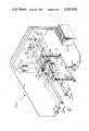
- FIG. 1is an isometric view of a wafer handling apparatus constructed in accordance with one embodiment of the invention.
- the wafer handling apparatustransports a silicon wafer to a work station, centers the wafer at the work station and bakes the wafer at the work station.
- FIGS. 2-A through 2-Care top plan views taken along the line and in the direction indicated by the arrows 2--2 in FIG. 1. These Figs. show a sequence of operations involved in forcing an off center wafer into center with the center of the work station prior to lifting of the wafer off of the conveyor belts by the wafer support members at the work station.
- FIG. 3is a fragmentary side elevation view, partly in cross section, taken along the line and in the direction indicated by the arrows 3--3 in FIG. 2-C, showing how the wafer is supported by the support members at the work station.
- FIG. 3shows how the support members engage the wafer only at peripheral areas on the under side of the wafer leaving the top surface and the edge of the wafer free of contact by the support members.
- FIG. 3also shows how the downstream support member has a vertical portion of greater height than the upstream support member for engagement with the wafer during the recentering operation shown in FIG. 2-B.
- FIG. 4is an enlarged isometric view of the downstream support member.
- FIG. 4shows the curved surface which permits the wafer to be rotated and shifted laterally until the wafer is centered in the operation illustrated in FIG. 2-B.
- FIGS. 5-A through 5-Care a sequence of views taken generally along the line and in the direction indicated by the arrows 5--5 in FIG. 1. These views show how a wafer may be heated, in one method of the present invention, by initially engaging the wafer in contact with the hot plate at the beginning of the cycle to obtain an initial, rapid transfer of heat from the hot plate to the wafer (FIG. 5-A) and then by lifting the wafer out of contact with the hot plate and thereafter repositioning the wafer with respect to the hot plate at varying distances (FIGS. 5-B and 5-C) to maintain an air gap between the wafer and the hot plate and to regulate the heating of the wafer as a function of the distance of the wafer from the hot plate.
- FIG. 6-Ais a graph showing three different wafer temperature vs. time profiles obtained in accordance with the present invention by varying the proximity of the wafer to the hot plate during the heating cycle.
- FIG. 6-Bis a graph showing the variation of distance of the wafer from the hot plate for each of the three wafer temperature vs. time profiles shown in FIG. 6-A.
- FIG. 7is a graph showing the variation of the heat flux between two constant-temperature parallel plates as a function of the thickness of a gas space between the plates.
- a wafer handling apparatus constructed in accordance with one embodiment of the present inventionis indicated generally by the reference numeral 11 in FIG. 1.
- the wafer handling apparatus 11 shown in FIG. 1includes a wafer transport mechanism 15 for carrying a wafer 13 (in the direction indicated by the block arrow 16) to and away from a work station 17, a wafer lift mechanism 18 for raising and lowering the wafer at the work station, a hot plate 20 for baking the wafer at the work station, and a controller 22 for controlling the operation of the wafer handling apparatus 11.
- the controller 22includes feedback means for adjusting the position of the wafer 13 with respect to the hot plate 20 in response to a measured temperature (as sensed by the temperature sensor 75 and as transmitted to the controller 22 on the line 77) to maintain a predetermined wafer temperature for each time interval of the heating cycle of the wafer.
- the controller 22also includes logic means which are operatively associated with the drive means 39 for slowing down substantially the speed of the two belts 21 and 23 and the speed at which the wafer 13 is conveyed into the heating station area in response to the detecting of the entrance of the wafer 13 into the heating station and for stopping the two belts 21 and 23 and the wafer 13 when the trailing part of the wafer 13 uncovers the optical paths of both of the two sensors 47 and 51 and the signals transmitted from the sensors to the controller 22 on the lines 53.
- This mode of operation of the feedback means and the logic means of the controller 22will become more apparent from the detailed description to follow.
- FIG. 1shows a silicon wafer 13 placed at the inlet end of the wafer transport mechanism 15 for transport to the work station 17.
- the wafer 13is a generally circular shaped wafer and usually has a flat 19 ground on the periphery.
- the wafer transport mechanism 15includes a pair of laterally spaced and parallel extending drive belts 21 and 23 trained over pulleys 25 and 27 at one end and over pulleys 29 and 31 at the other end.
- the belts 21 and 23are O ring belts.
- the O ring belt 21 and associated pulleys 25 and 29are mounted on a carriage 33; and the O ring belt 23 and associated pulleys 27 and 31 are mounted on a carriage 35.
- the carriages 33 and 35have inner surfaces which face the side edges of the wafer and which normally do not touch the wafer. However, if the wafer should be or become off center with respect to the centerline of the wafer transport system, the inner surfaces of the carriages 33 and 35 act as guides to push the center of the wafer back into alignment with the centerline of the wafer transport systems as the wafer is carried forward by the belts 21 and 23 toward the work station.
- a drive motor 39is connected to drive the pulleys 29 and 31.
- the details of the drive to the pulleys 29 and 31are shown in the U.S. Pat. No. 4,217,977.
- the controller 22controls the starting and stopping and the speed of rotation of the drive motor 39 through a line 43.
- a wafer position sensor 45 having an upwardly facing detector element 47is mounted on the carriage 33.
- the sensor 45is an optical sensor and the element 47 is a light responsive detector element.
- a similar wafer position sensor 49 having an upwardly facing light responsive detector element 51is mounted on the carriage 35.
- the sensors 45 and 49are connected to the controller 22 by lines 53 and 55.
- the O ring belts 21 and 23are driven at the same speed.
- the speedis a relatively fast speed until the wafer enters the work station area, as sensed by the sensors 45 and 49.
- the belts 21 and 23are then driven at a relatively slow speed until the wafer is centered in position over the center of the work station and the detectors 47 and 51 are uncovered by the back portion of the wafer. At that time the drive to the belts is stopped.
- the wafer lift mechanism 18comprises a pair of wafer support members, an upstream member 57 and a downstream member 59.
- the members 57 and 59are raised and lowered (in the direction indicated by the block arrows 61) to lift the wafer 13 off of the O ring belts 21 and 23 (prior to a wafer processing operation at the work station 17) and to lower the wafer 13 back onto the O ring belts 21 and 23 (after the completion of the wafer processing steps at the work station 17).
- the O ring belts 21 and 23are moved outwardly (to the dotted line positions illustrated in FIG. 1) after the wafer 13 has been lifted off of the belts, and the O ring belts 21 and 23 are moved inwardly (to the solid line position shown in FIG. 1) after the completion of the processing operations on the wafer at the work station when the wafer 13 is lowered back onto the belts for transport away from the work station 17.
- the sequence(lifting the wafer off of the belts 21 and 23, movement of the related carriages outwardly, lowering of the wafer at the work station 17 for a processing operation, raising of the wafer above the belts 21 and 23 at the completion of a processing operation, movement of the belts inwardly, and lowering of the wafer back onto the belts for subsequent transport of the wafer away from the work station 17) is like that described in the above noted U.S. Pat. No. 4,217,977 incorporated by reference in this application.
- the support members 57 and 59are connected to a yoke mechanism 63, and the vertical position of the yoke mechanism 63 is controlled by a linear actuator 65 connected to the controller 22 by a line 67.
- the work station 17 as shown in FIG. 1is a heating station and is used to perform a baking operation on the wafer 13.
- the heating station 17is used to perform any or all of the hard bake, soft bake and dehydration bake operations referred to above in the introductory part of this application.
- a hot plate 20is centrally positioned as illustrated in FIG. 1 at the heating station 17 to provide the heat for the bake operation on the wafer 13.
- the hot plate 20has a very large mass in comparison to the mass of the wafer, and the temperature of the hot plate is maintained at a constant temperature within narrow tolerances and at a level higher than the equilibrium or target temperature level to which the wafer is to be heated.
- the heating source for the hot plate 20is not shown but is, in a preferred embodiment of the present invention, an electrical heating source.
- a pyrometer 75is mounted above the heating station 17 for measuring the temperature of the wafer 13.
- the pyrometer 75in a preferred embodiment of the present invention measures the temperature by infrared radiation emitted from the heated wafer 13.
- the pyrometertransmits a signal indicating the measured temperature to the controller 22 by a line 77.
- the waferis heated by a proximity baking technique.
- the amount of heat transfered to the wafer and the rate at which the heat is transferred to the waferare determined by the distance between the wafer and the hot plate 20 and by the amount of time that the wafer is maintained at each distance from the hot plate.
- the hot plate 20Because the hot plate 20 has a large mass (a giant mass in comparison to the mass of the wafer) and is maintained at a temperature level higher than that of the highest temperature to which the wafer is to be heated, the hot plate 20 provides a constant temperature heating source which is easy to control and which, in effect, serves as an overdriven source.
- the control of the wafer temperature and the rate at which the wafer temperature is changedare dependent only on the proximity (the distance) between the wafer and the hot plate.
- the wafercan be placed in direct contact with the hot plate (as illustrated in FIG. 5-A), and this produces the fastest rate of heat transfer from the hot plate to the wafer.
- the wafer 13is held slightly above the hot plate and is separated from the hot plate by an air gap 79 of small thickness (as illustrated in FIG. 5-B).
- the rate at which heat is transferred to the waferis further reduced.
- the wafer temperature rise timevaries in the ways shown in the correspondingly numbered curves 1, 2, and 3 in FIG. 6-A.
- a fast rise timecan also be obtained without contacting the wafer with the hot plate.
- the primary mechanism of heat transferis conduction (as shown in FIG. 8); and (as shown in FIG. 7) a high amount of heat flux is transferred across a thin gap without direct contact.
- baking of the wafer without any contact with the hot plateis preferred to minimize the risk of contamination.
- the present inventionaccomodates baking without contact while still permiting a fast rise of temperature, if a fast rise is desired.
- the present inventionpermits the temperature-time profile either to be scheduled as a set of distance instructions supplied to the controller 22 or to be controlled by a temperature measuring servo technique for comparison with adherence to a time temperature profile instruction supplied to the controller 22.
- the actual temperature of the wafer(as measured by the pyrometer 75) is compared to the scheduled temperature for that point in time in the bake cycle, and the controller 22 signals a linear actuator 65 to make any necessary adjustment (either upwardly or downwardly) to reposition the wafer to conform the actual temperature to the scheduled temperature.
- the preferred range of control in the present inventionis within the range in which conduction provides a substantial contribution to the amount of heat transferred and in which convection provides either no contribution or substantially little contribution to the amount of heat transferred.
- control range for the spacing between the wafer and the hot plateis approximately 8 inches
- the linear actuator 65responds to electronic pulses from a microprocessor chip drive on a central processing unit board within the controller 22 to move the wafer support members 57 and 59 vertically up and down to any of approximately 500 discrete levels, spaced 0.002 inches apart.
- Proper centering of the center of the wafer with the center of the work stationis important in a wafer baking operation; and it is also important in other wafer processing operations, particularly those operations in which it is necessary to rotate the wafer.
- the wafer transport mechanism 15includes guides alongside the belts 21 and 23 for contacting the wafer 13 to put the center back on line in the event the center should become off line at some point in the transport on the belts 21 and 23.
- the present inventionalso incorporates a fail safe mechanism and mode of operation for centering the wafer at the work station 17 in the event the wafer should get off center at that point in the handling of the wafer.
- a fail safe mechanism and mode of operationfor centering the wafer at the work station 17 in the event the wafer should get off center at that point in the handling of the wafer.
- the recentering of the off center wafer 13 shown in FIG. 2-Ais accomplished by the co-action of the optical sensors 45 and 49, logic in the controller 22 which receives signals from the sensors, the drive of the belts 21 and 23, and a curved surface 87 on the downstream wafer support member 59.
- the leading portion of the wafer 13passes over the optical paths of the detectors 47 and 51 as the wafer is transported to the work station 17.
- the sensors 45 and 49then send signals to the controller (over the lines 53 and 55), and the controller 22 slows down the drive motor for the belts 21 and 23 substantially so that wafer 13 proceeds into the work station area at a relatively slow rate of speed.
- the sensors 45 and 49signal the controller 22, and the logic in the controller 22 shuts off the drive to the belts 21 and 23 so that the wafer 13 is stopped at the work station with its center 81 coincident with the center 85 of the work station.
- the use of two sensors in the present inventioninsures centering of the wafer regardless of the orientation of the flat 19 and insures that the wafer is centered at the work station in a way that is not possible with the use of a single sensor.
- the waferIn the orientation of the flat 19 shown in FIG. 2-A (with the flat at the 12 o'clock position) the wafer can be off-center by a maximum amount.
- the present inventiondetects this off-centering, and the two sensors function to insure that the wafer is properly centered at the work station as described in more detail below.
- the wafercould actually be on-center with the center line of the wafer transport apparatus, but might not be fully transported to the actual center of the work station if a single sensor (instead of the two sensors of the present invention) were used to control the drive of the belts. That is, if the flat 19 were at the 2 o'clock position and uncovered the single sensor at the work station, the wafer transport mechanism would stop before the center 81 of the wafer actually was moved over the center 85 of the work station.
- the use of two sensors in the present inventioninsures that exact coincidence centering of the center 81 of the wafer and the center 85 of the work station is always achieved, because both sensors must be uncovered before the drive is stopped.
- one of the detectorsin this case detector 47
- the drive to the beltsbeing continued (at the slow speed) until both of the detectors 47 and 51 are uncovered.
- the wafer 13is rotated (in the direction indicated by the block arrow 87 in FIG. 2-B). This occurs because the edge of the wafer 13 is engaged with that portion of the curved surface 87 of the downstream support member 59 which extends above the upper end of the upstream support 57. See FIG. 3 which shows this difference in height 89. This difference in height permits the wafer 13 to pass over the top of the wafer support member 57 and still contact the surface 87 of the downstream support member 59 if the wafer is off center at this point in the wafer handling process.
- the combination of the engagement of the edge of the wafer 81 with the curved surface 87, the shape of the curved surface 87 and the continued slow speed drive of the belts 21 and 23causes the wafer to be rotated and shifted laterally until the center 81 of the wafer is aligned with the center 85 of the work station 17 in the condition illustrated in FIG. 2-C. At this time both of the detectors 47 and 51 are uncovered, and the controller 22 stops the drive of the belts 21 and 23.
Landscapes
- Engineering & Computer Science (AREA)
- Microelectronics & Electronic Packaging (AREA)
- Condensed Matter Physics & Semiconductors (AREA)
- General Physics & Mathematics (AREA)
- Manufacturing & Machinery (AREA)
- Computer Hardware Design (AREA)
- Physics & Mathematics (AREA)
- Power Engineering (AREA)
- Container, Conveyance, Adherence, Positioning, Of Wafer (AREA)
- Control Of Conveyors (AREA)
- Exposure Of Semiconductors, Excluding Electron Or Ion Beam Exposure (AREA)
- Delivering By Means Of Belts And Rollers (AREA)
- Registering Or Overturning Sheets (AREA)
- Photosensitive Polymer And Photoresist Processing (AREA)
Abstract
Description
Claims (26)
Priority Applications (5)
| Application Number | Priority Date | Filing Date | Title |
|---|---|---|---|
| US06/479,197US4507078A (en) | 1983-03-28 | 1983-03-28 | Wafer handling apparatus and method |
| JP58185215AJPS59181617A (en) | 1983-03-28 | 1983-10-05 | Method and device for operating wafer |
| DE3402664ADE3402664C2 (en) | 1983-03-28 | 1984-01-24 | Method for treating and / or handling a wafer, device for carrying out the method and use of the method in wafer processing stations |
| GB08407962AGB2137414B (en) | 1983-03-28 | 1984-03-28 | Wafer transporting centring and heating |
| GB08622394AGB2180097B (en) | 1983-03-28 | 1986-09-17 | Wafer handling apparatus |
Applications Claiming Priority (1)
| Application Number | Priority Date | Filing Date | Title |
|---|---|---|---|
| US06/479,197US4507078A (en) | 1983-03-28 | 1983-03-28 | Wafer handling apparatus and method |
Publications (1)
| Publication Number | Publication Date |
|---|---|
| US4507078Atrue US4507078A (en) | 1985-03-26 |
Family
ID=23903046
Family Applications (1)
| Application Number | Title | Priority Date | Filing Date |
|---|---|---|---|
| US06/479,197Expired - LifetimeUS4507078A (en) | 1983-03-28 | 1983-03-28 | Wafer handling apparatus and method |
Country Status (4)
| Country | Link |
|---|---|
| US (1) | US4507078A (en) |
| JP (1) | JPS59181617A (en) |
| DE (1) | DE3402664C2 (en) |
| GB (2) | GB2137414B (en) |
Cited By (38)
| Publication number | Priority date | Publication date | Assignee | Title |
|---|---|---|---|---|
| US4698132A (en)* | 1986-09-30 | 1987-10-06 | Rca Corporation | Method of forming tapered contact openings |
| EP0257540A3 (en)* | 1986-08-23 | 1988-06-08 | British Steel Corporation | Processing steel slabs processing steel slabs |
| US4819167A (en)* | 1987-04-20 | 1989-04-04 | Applied Materials, Inc. | System and method for detecting the center of an integrated circuit wafer |
| US4862798A (en)* | 1985-11-04 | 1989-09-05 | American Screen Printing Equipment Company | Cylindrical object screen printer with object centering means |
| US5061144A (en)* | 1988-11-30 | 1991-10-29 | Tokyo Electron Limited | Resist process apparatus |
| US5226523A (en)* | 1989-09-26 | 1993-07-13 | Canon Kabushiki Kaisha | Conveying apparatus and method of controlling the same |
| US5252807A (en)* | 1990-07-02 | 1993-10-12 | George Chizinsky | Heated plate rapid thermal processor |
| US5267853A (en)* | 1991-10-15 | 1993-12-07 | Kabushiki Kaisha Shinkawa | Curing device |
| US5421446A (en)* | 1993-03-12 | 1995-06-06 | United Parcel Service Of America, Inc. | Article diverter apparatus for use in conveyor systems |
| US5848868A (en)* | 1996-04-22 | 1998-12-15 | Kabushiki Kaisha Shinkawa | Wafer conveying apparatus |
| US6133550A (en)* | 1996-03-22 | 2000-10-17 | Sandia Corporation | Method and apparatus for thermal processing of semiconductor substrates |
| US6140256A (en)* | 1995-11-28 | 2000-10-31 | Tokyo Electron Limited | Method and device for treating semiconductor with treating gas while substrate is heated |
| US6198074B1 (en) | 1996-09-06 | 2001-03-06 | Mattson Technology, Inc. | System and method for rapid thermal processing with transitional heater |
| US6221437B1 (en) | 1999-04-12 | 2001-04-24 | Reynolds Tech Fabricators, Inc. | Heated workpiece holder for wet plating bath |
| US6257567B1 (en)* | 1998-07-01 | 2001-07-10 | Kolbus Gmbh & Co. Kg | Conveying device for book binding machines |
| US6315512B1 (en) | 1997-11-28 | 2001-11-13 | Mattson Technology, Inc. | Systems and methods for robotic transfer of workpieces between a storage area and a processing chamber |
| US6403925B1 (en) | 1995-07-10 | 2002-06-11 | Mattson Technology, Inc. | System and method for thermal processing of a semiconductor substrate |
| US20030160401A1 (en)* | 2002-01-28 | 2003-08-28 | Kang Ki Sang | Centering mechanism, centering unit, semiconductor manufacturing apparatus, and centering method |
| US20040020601A1 (en)* | 2000-02-10 | 2004-02-05 | Applied Materials, Inc. | Process and an integrated tool for low k dielectric deposition including a pecvd capping module |
| US20040151574A1 (en)* | 2001-05-29 | 2004-08-05 | Zhimin Lu | Method and apparatus to correct wafer drift |
| US20040258514A1 (en)* | 2002-06-12 | 2004-12-23 | Ivo Raaijmakers | Semiconductor wafer position shift measurement and correction |
| US20050123387A1 (en)* | 2003-10-13 | 2005-06-09 | Hap Handhabungs-, Automatisierungs- Und Prazisionstechnik Gmbh | Apparatus for transporting and aligning disk-shaped elements |
| US20050192699A1 (en)* | 2004-02-26 | 2005-09-01 | Taiwan Semiconductor Manufacturing Co., Ltd. | Temperature-sensing wafer position detection system and method |
| US20060246390A1 (en)* | 2003-03-06 | 2006-11-02 | Michiro Aoki | Carrying mechanism using wire material, heat treating furnance using the mechanism, and heat treating method |
| US20070275639A1 (en)* | 2006-05-29 | 2007-11-29 | Fujikoshi Machinery Corp. | Workpiece centering apparatus and method of centering workpiece |
| US20070298188A1 (en)* | 2006-06-26 | 2007-12-27 | Tokyo Electron Limited | Substrate processing method and apparatus |
| US20080179378A1 (en)* | 1998-06-19 | 2008-07-31 | Makoto Imanishi | Method of forming bumps on a wafer utilizing a post-heating operation, and an apparatus therefore |
| US20090093906A1 (en)* | 2007-10-04 | 2009-04-09 | Asm Japan K.K. | Position sensor system for substrate transfer robot |
| US20090155452A1 (en)* | 2007-12-13 | 2009-06-18 | Asm Genitech Korea Ltd. | Thin film deposition apparatus and method thereof |
| US20090217871A1 (en)* | 2008-02-28 | 2009-09-03 | Asm Genitech Korea Ltd. | Thin film deposition apparatus and method of maintaining the same |
| US7963736B2 (en) | 2008-04-03 | 2011-06-21 | Asm Japan K.K. | Wafer processing apparatus with wafer alignment device |
| US20120245882A1 (en)* | 2011-03-25 | 2012-09-27 | Macronix International Co., Ltd. | Wafer tilt detection system |
| JP2013058546A (en)* | 2011-09-07 | 2013-03-28 | Nippon Electric Glass Co Ltd | Plate glass positioning device and its positioning method |
| WO2015000520A1 (en)* | 2013-07-04 | 2015-01-08 | Ev Group E. Thallner Gmbh | Method and device for treating a substrate surface |
| US9196518B1 (en) | 2013-03-15 | 2015-11-24 | Persimmon Technologies, Corp. | Adaptive placement system and method |
| US10058996B2 (en) | 2014-11-18 | 2018-08-28 | Persimmon Technologies Corporation | Robot adaptive placement system with end-effector position estimation |
| US20190013215A1 (en)* | 2017-07-05 | 2019-01-10 | Kawasaki Jukogyo Kabushiki Kaisha | Substrate holding hand and substrate conveying apparatus including the same |
| US11858755B2 (en)* | 2020-02-06 | 2024-01-02 | Murata Machinery, Ltd. | Gripping apparatus and stacker |
Families Citing this family (16)
| Publication number | Priority date | Publication date | Assignee | Title |
|---|---|---|---|---|
| JPS6160509A (en)* | 1984-08-31 | 1986-03-28 | Fujitsu Ltd | Conveyance device |
| JPH0121563Y2 (en)* | 1986-03-26 | 1989-06-27 | ||
| FR2610450A1 (en)* | 1987-01-29 | 1988-08-05 | France Etat | DEVICE FOR HEAT TREATING SEMICONDUCTOR WAFERS |
| JPS63308337A (en)* | 1987-06-10 | 1988-12-15 | Teru Kyushu Kk | Spinner |
| JP2611251B2 (en)* | 1987-08-28 | 1997-05-21 | 株式会社ニコン | Substrate transfer device |
| IL86514A0 (en)* | 1988-05-26 | 1988-11-15 | ||
| CH680275A5 (en)* | 1990-03-05 | 1992-07-31 | Tet Techno Investment Trust | |
| JP2704309B2 (en)* | 1990-06-12 | 1998-01-26 | 大日本スクリーン製造株式会社 | Substrate processing apparatus and substrate heat treatment method |
| JP2638668B2 (en)* | 1990-09-03 | 1997-08-06 | 大日本スクリーン製造株式会社 | Substrate transfer method and substrate transfer device |
| DE4125877C2 (en)* | 1991-08-05 | 1994-12-22 | Forschungszentrum Juelich Gmbh | Receiving device for samples to be introduced into an apparatus via a transfer mechanism |
| GB2266992A (en)* | 1992-05-06 | 1993-11-17 | Surface Tech Sys Ltd | Apparatus for loading semi-conductor wafers |
| DE69329269T2 (en)* | 1992-11-12 | 2000-12-28 | Applied Materials, Inc. | System and method for automatic positioning of a substrate in a process room |
| KR100275723B1 (en)* | 1997-10-24 | 2001-01-15 | 윤종용 | Oven with hot plate with adjustable height of spacer |
| DE19748088A1 (en)* | 1997-10-30 | 1999-05-12 | Wacker Siltronic Halbleitermat | Method and device for detecting a misalignment of a semiconductor wafer |
| US6629053B1 (en) | 1999-11-22 | 2003-09-30 | Lam Research Corporation | Method and apparatus for determining substrate offset using optimization techniques |
| US6502054B1 (en) | 1999-11-22 | 2002-12-31 | Lam Research Corporation | Method of and apparatus for dynamic alignment of substrates |
Citations (4)
| Publication number | Priority date | Publication date | Assignee | Title |
|---|---|---|---|---|
| US3044297A (en)* | 1960-09-15 | 1962-07-17 | Industrial Nucleonics Corp | Measuring system |
| US3870460A (en)* | 1974-04-03 | 1975-03-11 | Gca Corp | Single or multi-track fluid bearing heating apparatus and method |
| US4217977A (en)* | 1978-09-15 | 1980-08-19 | The Silicon Valley Group, Inc. | Conveyor system |
| US4276603A (en)* | 1979-10-30 | 1981-06-30 | Btu Engineering Corporation | Diffusion furnace microcontroller |
Family Cites Families (3)
| Publication number | Priority date | Publication date | Assignee | Title |
|---|---|---|---|---|
| US4040512A (en)* | 1976-01-12 | 1977-08-09 | Ness Warren C | Method of and means for indexing articles |
| JPS5539021A (en)* | 1978-09-14 | 1980-03-18 | Hitachi Electronics Eng Co Ltd | Automatic plate tester |
| DE2924526A1 (en)* | 1979-06-18 | 1981-01-08 | Siemens Ag | MONOLITHICALLY INTEGRATED SEMICONDUCTOR MEMORY |
- 1983
- 1983-03-28USUS06/479,197patent/US4507078A/ennot_activeExpired - Lifetime
- 1983-10-05JPJP58185215Apatent/JPS59181617A/enactiveGranted
- 1984
- 1984-01-24DEDE3402664Apatent/DE3402664C2/ennot_activeExpired - Fee Related
- 1984-03-28GBGB08407962Apatent/GB2137414B/ennot_activeExpired
- 1986
- 1986-09-17GBGB08622394Apatent/GB2180097B/ennot_activeExpired
Patent Citations (4)
| Publication number | Priority date | Publication date | Assignee | Title |
|---|---|---|---|---|
| US3044297A (en)* | 1960-09-15 | 1962-07-17 | Industrial Nucleonics Corp | Measuring system |
| US3870460A (en)* | 1974-04-03 | 1975-03-11 | Gca Corp | Single or multi-track fluid bearing heating apparatus and method |
| US4217977A (en)* | 1978-09-15 | 1980-08-19 | The Silicon Valley Group, Inc. | Conveyor system |
| US4276603A (en)* | 1979-10-30 | 1981-06-30 | Btu Engineering Corporation | Diffusion furnace microcontroller |
Cited By (57)
| Publication number | Priority date | Publication date | Assignee | Title |
|---|---|---|---|---|
| US4862798A (en)* | 1985-11-04 | 1989-09-05 | American Screen Printing Equipment Company | Cylindrical object screen printer with object centering means |
| EP0257540A3 (en)* | 1986-08-23 | 1988-06-08 | British Steel Corporation | Processing steel slabs processing steel slabs |
| US4698132A (en)* | 1986-09-30 | 1987-10-06 | Rca Corporation | Method of forming tapered contact openings |
| US4819167A (en)* | 1987-04-20 | 1989-04-04 | Applied Materials, Inc. | System and method for detecting the center of an integrated circuit wafer |
| US5061144A (en)* | 1988-11-30 | 1991-10-29 | Tokyo Electron Limited | Resist process apparatus |
| US5226523A (en)* | 1989-09-26 | 1993-07-13 | Canon Kabushiki Kaisha | Conveying apparatus and method of controlling the same |
| US5252807A (en)* | 1990-07-02 | 1993-10-12 | George Chizinsky | Heated plate rapid thermal processor |
| US5267853A (en)* | 1991-10-15 | 1993-12-07 | Kabushiki Kaisha Shinkawa | Curing device |
| US5421446A (en)* | 1993-03-12 | 1995-06-06 | United Parcel Service Of America, Inc. | Article diverter apparatus for use in conveyor systems |
| US6403925B1 (en) | 1995-07-10 | 2002-06-11 | Mattson Technology, Inc. | System and method for thermal processing of a semiconductor substrate |
| US6140256A (en)* | 1995-11-28 | 2000-10-31 | Tokyo Electron Limited | Method and device for treating semiconductor with treating gas while substrate is heated |
| US6133550A (en)* | 1996-03-22 | 2000-10-17 | Sandia Corporation | Method and apparatus for thermal processing of semiconductor substrates |
| US6355909B1 (en) | 1996-03-22 | 2002-03-12 | Sandia Corporation | Method and apparatus for thermal processing of semiconductor substrates |
| US5848868A (en)* | 1996-04-22 | 1998-12-15 | Kabushiki Kaisha Shinkawa | Wafer conveying apparatus |
| US6331697B2 (en) | 1996-09-06 | 2001-12-18 | Mattson Technology Inc. | System and method for rapid thermal processing |
| US6198074B1 (en) | 1996-09-06 | 2001-03-06 | Mattson Technology, Inc. | System and method for rapid thermal processing with transitional heater |
| US20040091349A1 (en)* | 1997-11-28 | 2004-05-13 | Farzad Tabrizi | Methods for transporting wafers for vacuum processing |
| US6647665B1 (en) | 1997-11-28 | 2003-11-18 | Mattson Technology, Inc. | Door systems for low contamination, high throughput handling of workpieces for vacuum processing |
| US6315512B1 (en) | 1997-11-28 | 2001-11-13 | Mattson Technology, Inc. | Systems and methods for robotic transfer of workpieces between a storage area and a processing chamber |
| US6568552B1 (en) | 1997-11-28 | 2003-05-27 | Mattson Technology, Inc. | Systems and methods for low contamination, high throughput handling of workpieces for vacuum processing |
| US20080179378A1 (en)* | 1998-06-19 | 2008-07-31 | Makoto Imanishi | Method of forming bumps on a wafer utilizing a post-heating operation, and an apparatus therefore |
| US6257567B1 (en)* | 1998-07-01 | 2001-07-10 | Kolbus Gmbh & Co. Kg | Conveying device for book binding machines |
| US6221437B1 (en) | 1999-04-12 | 2001-04-24 | Reynolds Tech Fabricators, Inc. | Heated workpiece holder for wet plating bath |
| US20040020601A1 (en)* | 2000-02-10 | 2004-02-05 | Applied Materials, Inc. | Process and an integrated tool for low k dielectric deposition including a pecvd capping module |
| US20040151574A1 (en)* | 2001-05-29 | 2004-08-05 | Zhimin Lu | Method and apparatus to correct wafer drift |
| US7008802B2 (en) | 2001-05-29 | 2006-03-07 | Asm America, Inc. | Method and apparatus to correct water drift |
| US20030160401A1 (en)* | 2002-01-28 | 2003-08-28 | Kang Ki Sang | Centering mechanism, centering unit, semiconductor manufacturing apparatus, and centering method |
| US7153087B2 (en)* | 2002-01-28 | 2006-12-26 | Samsung Electronics Co., Ltd. | Centering mechanism, centering unit, semiconductor manufacturing apparatus, and centering method |
| US20040258514A1 (en)* | 2002-06-12 | 2004-12-23 | Ivo Raaijmakers | Semiconductor wafer position shift measurement and correction |
| US7248931B2 (en) | 2002-06-12 | 2007-07-24 | Asm America, Inc. | Semiconductor wafer position shift measurement and correction |
| US6900877B2 (en) | 2002-06-12 | 2005-05-31 | Asm American, Inc. | Semiconductor wafer position shift measurement and correction |
| US20060246390A1 (en)* | 2003-03-06 | 2006-11-02 | Michiro Aoki | Carrying mechanism using wire material, heat treating furnance using the mechanism, and heat treating method |
| US20050123387A1 (en)* | 2003-10-13 | 2005-06-09 | Hap Handhabungs-, Automatisierungs- Und Prazisionstechnik Gmbh | Apparatus for transporting and aligning disk-shaped elements |
| US20050192699A1 (en)* | 2004-02-26 | 2005-09-01 | Taiwan Semiconductor Manufacturing Co., Ltd. | Temperature-sensing wafer position detection system and method |
| US6980876B2 (en)* | 2004-02-26 | 2005-12-27 | Taiwan Semiconductor Manufacturing Co., Ltd. | Temperature-sensing wafer position detection system and method |
| US7524232B2 (en)* | 2006-05-29 | 2009-04-28 | Fujikoshi Machinery Corp. | Workpiece centering apparatus and method of centering workpiece |
| US20070275639A1 (en)* | 2006-05-29 | 2007-11-29 | Fujikoshi Machinery Corp. | Workpiece centering apparatus and method of centering workpiece |
| US20070298188A1 (en)* | 2006-06-26 | 2007-12-27 | Tokyo Electron Limited | Substrate processing method and apparatus |
| US8181356B2 (en) | 2006-06-26 | 2012-05-22 | Tokyo Electron Limited | Substrate processing method |
| US7877895B2 (en)* | 2006-06-26 | 2011-02-01 | Tokyo Electron Limited | Substrate processing apparatus |
| US8041450B2 (en) | 2007-10-04 | 2011-10-18 | Asm Japan K.K. | Position sensor system for substrate transfer robot |
| US20090093906A1 (en)* | 2007-10-04 | 2009-04-09 | Asm Japan K.K. | Position sensor system for substrate transfer robot |
| US20090155452A1 (en)* | 2007-12-13 | 2009-06-18 | Asm Genitech Korea Ltd. | Thin film deposition apparatus and method thereof |
| US8347813B2 (en) | 2007-12-13 | 2013-01-08 | Asm Genitech Korea Ltd. | Thin film deposition apparatus and method thereof |
| US20090217871A1 (en)* | 2008-02-28 | 2009-09-03 | Asm Genitech Korea Ltd. | Thin film deposition apparatus and method of maintaining the same |
| US8273178B2 (en) | 2008-02-28 | 2012-09-25 | Asm Genitech Korea Ltd. | Thin film deposition apparatus and method of maintaining the same |
| US7963736B2 (en) | 2008-04-03 | 2011-06-21 | Asm Japan K.K. | Wafer processing apparatus with wafer alignment device |
| US20120245882A1 (en)* | 2011-03-25 | 2012-09-27 | Macronix International Co., Ltd. | Wafer tilt detection system |
| JP2013058546A (en)* | 2011-09-07 | 2013-03-28 | Nippon Electric Glass Co Ltd | Plate glass positioning device and its positioning method |
| US9196518B1 (en) | 2013-03-15 | 2015-11-24 | Persimmon Technologies, Corp. | Adaptive placement system and method |
| WO2015000520A1 (en)* | 2013-07-04 | 2015-01-08 | Ev Group E. Thallner Gmbh | Method and device for treating a substrate surface |
| CN105340073A (en)* | 2013-07-04 | 2016-02-17 | Ev集团E·索尔纳有限责任公司 | Method and device for treating a substrate surface |
| US20160126085A1 (en)* | 2013-07-04 | 2016-05-05 | Ev Group E. Thallner Gmbh | Method and device for treating a substrate surface |
| TWI619160B (en)* | 2013-07-04 | 2018-03-21 | Ev集團E塔那有限公司 | Method and device for treatment of a substrate surface |
| US10058996B2 (en) | 2014-11-18 | 2018-08-28 | Persimmon Technologies Corporation | Robot adaptive placement system with end-effector position estimation |
| US20190013215A1 (en)* | 2017-07-05 | 2019-01-10 | Kawasaki Jukogyo Kabushiki Kaisha | Substrate holding hand and substrate conveying apparatus including the same |
| US11858755B2 (en)* | 2020-02-06 | 2024-01-02 | Murata Machinery, Ltd. | Gripping apparatus and stacker |
Also Published As
| Publication number | Publication date |
|---|---|
| DE3402664C2 (en) | 1994-12-08 |
| JPH0145975B2 (en) | 1989-10-05 |
| GB2180097B (en) | 1987-09-09 |
| GB2137414B (en) | 1987-06-17 |
| DE3402664A1 (en) | 1984-10-04 |
| GB8622394D0 (en) | 1986-10-22 |
| GB2180097A (en) | 1987-03-18 |
| GB8407962D0 (en) | 1984-05-10 |
| JPS59181617A (en) | 1984-10-16 |
| GB2137414A (en) | 1984-10-03 |
Similar Documents
| Publication | Publication Date | Title |
|---|---|---|
| US4507078A (en) | Wafer handling apparatus and method | |
| KR101145511B1 (en) | Calibration of high speed loader to substrate transport system | |
| EP0063289B1 (en) | Apparatus for aligning a wafer | |
| US6643564B2 (en) | Method of determining retreat permission position of carrier arm and teaching device thereof | |
| US4024944A (en) | Semiconductor slice prealignment system | |
| KR101934657B1 (en) | Substrate processing device and substrate processing method | |
| US5409348A (en) | Substrate transfer method | |
| KR20190051816A (en) | Substrate transferring-and-receiving system and substrate transferring-and-receiving method | |
| JPH08335622A (en) | Substrate conveyer | |
| GB2194500A (en) | A wafer handling apparatus | |
| CN115985807A (en) | Substrate processing apparatus | |
| US4615521A (en) | Elevator between transfer passages | |
| JPH06246658A (en) | Substrate conveyer | |
| CN110718482A (en) | Heat treatment apparatus and substrate slip detection method | |
| JPH05304196A (en) | Wafer conveyor | |
| CN217293193U (en) | Feeding machine with preheating function | |
| KR0141476B1 (en) | Vertical heat treatment apparatus having wafer transfer mechanism and method for transferring wafers | |
| JPH075055Y2 (en) | Positioning stop device for the carrier | |
| JPH07121765B2 (en) | Transport device for automatic assembly | |
| JPH06124885A (en) | Rotating processor | |
| JPH11204429A (en) | Wafer processing device | |
| KR20050120281A (en) | Wafer algner | |
| JPH07142377A (en) | Treatment device | |
| JPS6052437A (en) | Wafer processing apparatus | |
| JP2023059818A (en) | Substrate processing equipment |
Legal Events
| Date | Code | Title | Description |
|---|---|---|---|
| AS | Assignment | Owner name:SILICON VALLEY GROUP INC., 3901 BURTON DRIVE, SANT Free format text:ASSIGNMENT OF ASSIGNORS INTEREST.;ASSIGNORS:TAM, JOHANN;ASHJAEE, JALAL;KUWAKI, NOBUO B.;AND OTHERS;REEL/FRAME:004137/0218 Effective date:19830324 | |
| STCF | Information on status: patent grant | Free format text:PATENTED CASE | |
| FEPP | Fee payment procedure | Free format text:PAYOR NUMBER ASSIGNED (ORIGINAL EVENT CODE: ASPN); ENTITY STATUS OF PATENT OWNER: SMALL ENTITY | |
| FPAY | Fee payment | Year of fee payment:4 | |
| AS | Assignment | Owner name:BANK OF AMERICA NATIONAL TRUST AND SAVINGS ASSOCIA Free format text:SECURITY INTEREST;ASSIGNOR:SILICON VALLEY GROUP, INC.;REEL/FRAME:005443/0382 Effective date:19900515 | |
| AS | Assignment | Owner name:BANK OF AMERICA NATIONAL TRUST AND SAVINGS ASSOCIA Free format text:SECURITY INTEREST;ASSIGNOR:SILICON VALLEY GROUP, IN.,;REEL/FRAME:005458/0172 Effective date:19900905 | |
| REMI | Maintenance fee reminder mailed | ||
| AS | Assignment | Owner name:SILICON VALLEY GROUP, INC., CALIFORNIA Free format text:RELEASED BY SECURED PARTY;ASSIGNOR:BANK OF AMERICA NATIONAL TRUST AND SAVINGS ASSOCIATION;REEL/FRAME:006396/0698 Effective date:19921103 | |
| AS | Assignment | Owner name:BARCLAYS BANK PLC, AS COLLATERAL AGENT, CALIFORNIA Free format text:SECURITY INTEREST;ASSIGNOR:SILICON VALLEY GROUP, INC.;REEL/FRAME:006437/0257 Effective date:19921103 | |
| FPAY | Fee payment | Year of fee payment:8 | |
| SULP | Surcharge for late payment | ||
| AS | Assignment | Owner name:SILICON VALLEY GROUP, INC., CALIFORNIA Free format text:RELEASE OF SECURITY INTEREST;ASSIGNOR:BARCLAYS BANK PLC, AS COLLATERAL AGENT;REEL/FRAME:007179/0198 Effective date:19941011 Owner name:ABN AMRO BANK N.V., AS AGENT, CALIFORNIA Free format text:SECURITY INTEREST;ASSIGNOR:SILICON VALLEY GROUP, INC.;REEL/FRAME:007179/0189 Effective date:19941007 | |
| REMI | Maintenance fee reminder mailed | ||
| FPAY | Fee payment | Year of fee payment:12 | |
| SULP | Surcharge for late payment |