US4502914A - Method of making structures with dimensions in the sub-micrometer range - Google Patents
Method of making structures with dimensions in the sub-micrometer rangeDownload PDFInfo
- Publication number
- US4502914A US4502914AUS06/546,612US54661283AUS4502914AUS 4502914 AUS4502914 AUS 4502914AUS 54661283 AUS54661283 AUS 54661283AUS 4502914 AUS4502914 AUS 4502914A
- Authority
- US
- United States
- Prior art keywords
- layer
- polymeric
- mask
- sidewall
- silicon
- Prior art date
- Legal status (The legal status is an assumption and is not a legal conclusion. Google has not performed a legal analysis and makes no representation as to the accuracy of the status listed.)
- Expired - Lifetime
Links
- 238000004519manufacturing processMethods0.000titleclaimsabstractdescription11
- VYPSYNLAJGMNEJ-UHFFFAOYSA-NSilicium dioxideChemical classO=[Si]=OVYPSYNLAJGMNEJ-UHFFFAOYSA-N0.000claimsabstractdescription203
- 239000010410layerSubstances0.000claimsabstractdescription170
- 238000000034methodMethods0.000claimsabstractdescription115
- 229910052581Si3N4Inorganic materials0.000claimsabstractdescription73
- HQVNEWCFYHHQES-UHFFFAOYSA-Nsilicon nitrideChemical compoundN12[Si]34N5[Si]62N3[Si]51N64HQVNEWCFYHHQES-UHFFFAOYSA-N0.000claimsabstractdescription72
- 239000000463materialSubstances0.000claimsabstractdescription69
- 239000000758substrateSubstances0.000claimsabstractdescription53
- XUIMIQQOPSSXEZ-UHFFFAOYSA-NSiliconChemical compound[Si]XUIMIQQOPSSXEZ-UHFFFAOYSA-N0.000claimsabstractdescription52
- 229910052710siliconInorganic materials0.000claimsabstractdescription52
- 239000010703siliconSubstances0.000claimsabstractdescription52
- 238000001020plasma etchingMethods0.000claimsabstractdescription47
- 238000002955isolationMethods0.000claimsabstractdescription36
- 239000013047polymeric layerSubstances0.000claimsabstractdescription36
- 230000003647oxidationEffects0.000claimsabstractdescription26
- 238000007254oxidation reactionMethods0.000claimsabstractdescription26
- 239000004642PolyimideSubstances0.000claimsabstractdescription17
- 229920001721polyimidePolymers0.000claimsabstractdescription17
- 238000001459lithographyMethods0.000claimsabstractdescription14
- 235000012239silicon dioxideNutrition0.000claimsdescription99
- 239000000377silicon dioxideSubstances0.000claimsdescription93
- 238000005530etchingMethods0.000claimsdescription50
- 238000000151depositionMethods0.000claimsdescription23
- 229920002120photoresistant polymerPolymers0.000claimsdescription19
- 239000001301oxygenSubstances0.000claimsdescription18
- 229910052760oxygenInorganic materials0.000claimsdescription18
- QVGXLLKOCUKJST-UHFFFAOYSA-Natomic oxygenChemical compound[O]QVGXLLKOCUKJST-UHFFFAOYSA-N0.000claimsdescription17
- XKRFYHLGVUSROY-UHFFFAOYSA-NArgonChemical compound[Ar]XKRFYHLGVUSROY-UHFFFAOYSA-N0.000claimsdescription14
- 238000004544sputter depositionMethods0.000claimsdescription12
- 230000008021depositionEffects0.000claimsdescription9
- QGZKDVFQNNGYKY-UHFFFAOYSA-NAmmoniaChemical compoundNQGZKDVFQNNGYKY-UHFFFAOYSA-N0.000claimsdescription8
- BLRPTPMANUNPDV-UHFFFAOYSA-NSilaneChemical compound[SiH4]BLRPTPMANUNPDV-UHFFFAOYSA-N0.000claimsdescription8
- 229910052786argonInorganic materials0.000claimsdescription7
- 239000003989dielectric materialSubstances0.000claimsdescription7
- 230000000694effectsEffects0.000claimsdescription6
- 229910000077silaneInorganic materials0.000claimsdescription6
- 229910021529ammoniaInorganic materials0.000claimsdescription4
- XPDWGBQVDMORPB-UHFFFAOYSA-NFluoroformChemical compoundFC(F)FXPDWGBQVDMORPB-UHFFFAOYSA-N0.000claimsdescription3
- 238000007740vapor depositionMethods0.000claimsdescription2
- 230000002411adverseEffects0.000claims5
- 239000004065semiconductorSubstances0.000abstractdescription14
- 229910052814silicon oxideInorganic materials0.000abstractdescription8
- 238000005516engineering processMethods0.000abstractdescription4
- 229920002994synthetic fiberPolymers0.000abstractdescription3
- TXEYQDLBPFQVAA-UHFFFAOYSA-NtetrafluoromethaneChemical compoundFC(F)(F)FTXEYQDLBPFQVAA-UHFFFAOYSA-N0.000description14
- 229910021420polycrystalline siliconInorganic materials0.000description12
- 229920005591polysiliconPolymers0.000description12
- 150000004767nitridesChemical class0.000description11
- 238000009792diffusion processMethods0.000description7
- 239000012212insulatorSubstances0.000description7
- 239000010453quartzSubstances0.000description7
- KZBUYRJDOAKODT-UHFFFAOYSA-NChlorineChemical compoundClClKZBUYRJDOAKODT-UHFFFAOYSA-N0.000description5
- 238000001039wet etchingMethods0.000description5
- 241000293849CordylanthusSpecies0.000description4
- KRHYYFGTRYWZRS-UHFFFAOYSA-NFluoraneChemical compoundFKRHYYFGTRYWZRS-UHFFFAOYSA-N0.000description4
- 238000005229chemical vapour depositionMethods0.000description4
- 239000004020conductorSubstances0.000description4
- 230000007547defectEffects0.000description4
- 239000007789gasSubstances0.000description4
- 230000010354integrationEffects0.000description4
- 238000004528spin coatingMethods0.000description4
- 238000007796conventional methodMethods0.000description3
- 238000011161developmentMethods0.000description3
- 230000018109developmental processEffects0.000description3
- 229910052751metalInorganic materials0.000description3
- 239000002184metalSubstances0.000description3
- KXGFMDJXCMQABM-UHFFFAOYSA-N2-methoxy-6-methylphenolChemical compound[CH]OC1=CC=CC([CH])=C1OKXGFMDJXCMQABM-UHFFFAOYSA-N0.000description2
- ZAMOUSCENKQFHK-UHFFFAOYSA-NChlorine atomChemical compound[Cl]ZAMOUSCENKQFHK-UHFFFAOYSA-N0.000description2
- XMIJDTGORVPYLW-UHFFFAOYSA-N[SiH2]Chemical compound[SiH2]XMIJDTGORVPYLW-UHFFFAOYSA-N0.000description2
- FRIKWZARTBPWBN-UHFFFAOYSA-N[Si].O=[Si]=OChemical compound[Si].O=[Si]=OFRIKWZARTBPWBN-UHFFFAOYSA-N0.000description2
- 239000000460chlorineSubstances0.000description2
- 229910052801chlorineInorganic materials0.000description2
- 230000005669field effectEffects0.000description2
- 239000001307heliumSubstances0.000description2
- 229910052734heliumInorganic materials0.000description2
- SWQJXJOGLNCZEY-UHFFFAOYSA-Nhelium atomChemical compound[He]SWQJXJOGLNCZEY-UHFFFAOYSA-N0.000description2
- 150000002500ionsChemical class0.000description2
- 150000002739metalsChemical class0.000description2
- 239000000203mixtureSubstances0.000description2
- 229920001568phenolic resinPolymers0.000description2
- 229920000642polymerPolymers0.000description2
- 230000005855radiationEffects0.000description2
- 238000010405reoxidation reactionMethods0.000description2
- 239000010409thin filmSubstances0.000description2
- PXGOKWXKJXAPGV-UHFFFAOYSA-NFluorineChemical compoundFFPXGOKWXKJXAPGV-UHFFFAOYSA-N0.000description1
- CERQOIWHTDAKMF-UHFFFAOYSA-MMethacrylateChemical compoundCC(=C)C([O-])=OCERQOIWHTDAKMF-UHFFFAOYSA-M0.000description1
- 229930192627NaphthoquinoneNatural products0.000description1
- 229910004014SiF4Inorganic materials0.000description1
- 238000001015X-ray lithographyMethods0.000description1
- 230000004888barrier functionEffects0.000description1
- 229910052681coesiteInorganic materials0.000description1
- 229910052906cristobaliteInorganic materials0.000description1
- 238000004132cross linkingMethods0.000description1
- 230000003247decreasing effectEffects0.000description1
- 238000005137deposition processMethods0.000description1
- 238000001312dry etchingMethods0.000description1
- 239000010408filmSubstances0.000description1
- 239000011737fluorineSubstances0.000description1
- 229910052731fluorineInorganic materials0.000description1
- 238000007429general methodMethods0.000description1
- 239000011521glassSubstances0.000description1
- 239000012535impuritySubstances0.000description1
- CPLXHLVBOLITMK-UHFFFAOYSA-Nmagnesium oxideInorganic materials[Mg]=OCPLXHLVBOLITMK-UHFFFAOYSA-N0.000description1
- 239000000395magnesium oxideSubstances0.000description1
- AXZKOIWUVFPNLO-UHFFFAOYSA-Nmagnesium;oxygen(2-)Chemical compound[O-2].[Mg+2]AXZKOIWUVFPNLO-UHFFFAOYSA-N0.000description1
- QVEIBLDXZNGPHR-UHFFFAOYSA-Nnaphthalene-1,4-dione;diazideChemical compound[N-]=[N+]=[N-].[N-]=[N+]=[N-].C1=CC=C2C(=O)C=CC(=O)C2=C1QVEIBLDXZNGPHR-UHFFFAOYSA-N0.000description1
- 150000002791naphthoquinonesChemical class0.000description1
- 230000003287optical effectEffects0.000description1
- TWNQGVIAIRXVLR-UHFFFAOYSA-Noxo(oxoalumanyloxy)alumaneChemical compoundO=[Al]O[Al]=OTWNQGVIAIRXVLR-UHFFFAOYSA-N0.000description1
- -1oxygen ionsChemical class0.000description1
- 238000000206photolithographyMethods0.000description1
- 238000012545processingMethods0.000description1
- 230000001681protective effectEffects0.000description1
- 239000011241protective layerSubstances0.000description1
- ABTOQLMXBSRXSM-UHFFFAOYSA-Nsilicon tetrafluorideChemical compoundF[Si](F)(F)FABTOQLMXBSRXSM-UHFFFAOYSA-N0.000description1
- 229910052682stishoviteInorganic materials0.000description1
- BDHFUVZGWQCTTF-UHFFFAOYSA-MsulfonateChemical compound[O-]S(=O)=OBDHFUVZGWQCTTF-UHFFFAOYSA-M0.000description1
- SFZCNBIFKDRMGX-UHFFFAOYSA-Nsulfur hexafluorideChemical compoundFS(F)(F)(F)(F)FSFZCNBIFKDRMGX-UHFFFAOYSA-N0.000description1
- 229910052905tridymiteInorganic materials0.000description1
Images


Classifications
- H—ELECTRICITY
- H01—ELECTRIC ELEMENTS
- H01L—SEMICONDUCTOR DEVICES NOT COVERED BY CLASS H10
- H01L21/00—Processes or apparatus adapted for the manufacture or treatment of semiconductor or solid state devices or of parts thereof
- H01L21/02—Manufacture or treatment of semiconductor devices or of parts thereof
- H01L21/027—Making masks on semiconductor bodies for further photolithographic processing not provided for in group H01L21/18 or H01L21/34
- H01L21/033—Making masks on semiconductor bodies for further photolithographic processing not provided for in group H01L21/18 or H01L21/34 comprising inorganic layers
- H01L21/0334—Making masks on semiconductor bodies for further photolithographic processing not provided for in group H01L21/18 or H01L21/34 comprising inorganic layers characterised by their size, orientation, disposition, behaviour, shape, in horizontal or vertical plane
- H01L21/0337—Making masks on semiconductor bodies for further photolithographic processing not provided for in group H01L21/18 or H01L21/34 comprising inorganic layers characterised by their size, orientation, disposition, behaviour, shape, in horizontal or vertical plane characterised by the process involved to create the mask, e.g. lift-off masks, sidewalls, or to modify the mask, e.g. pre-treatment, post-treatment
- H—ELECTRICITY
- H01—ELECTRIC ELEMENTS
- H01L—SEMICONDUCTOR DEVICES NOT COVERED BY CLASS H10
- H01L21/00—Processes or apparatus adapted for the manufacture or treatment of semiconductor or solid state devices or of parts thereof
- H01L21/02—Manufacture or treatment of semiconductor devices or of parts thereof
- H01L21/027—Making masks on semiconductor bodies for further photolithographic processing not provided for in group H01L21/18 or H01L21/34
- H01L21/033—Making masks on semiconductor bodies for further photolithographic processing not provided for in group H01L21/18 or H01L21/34 comprising inorganic layers
- H01L21/0334—Making masks on semiconductor bodies for further photolithographic processing not provided for in group H01L21/18 or H01L21/34 comprising inorganic layers characterised by their size, orientation, disposition, behaviour, shape, in horizontal or vertical plane
- H01L21/0338—Process specially adapted to improve the resolution of the mask
- H—ELECTRICITY
- H01—ELECTRIC ELEMENTS
- H01L—SEMICONDUCTOR DEVICES NOT COVERED BY CLASS H10
- H01L21/00—Processes or apparatus adapted for the manufacture or treatment of semiconductor or solid state devices or of parts thereof
- H01L21/02—Manufacture or treatment of semiconductor devices or of parts thereof
- H01L21/04—Manufacture or treatment of semiconductor devices or of parts thereof the devices having potential barriers, e.g. a PN junction, depletion layer or carrier concentration layer
- H01L21/18—Manufacture or treatment of semiconductor devices or of parts thereof the devices having potential barriers, e.g. a PN junction, depletion layer or carrier concentration layer the devices having semiconductor bodies comprising elements of Group IV of the Periodic Table or AIIIBV compounds with or without impurities, e.g. doping materials
- H01L21/30—Treatment of semiconductor bodies using processes or apparatus not provided for in groups H01L21/20 - H01L21/26
- H01L21/302—Treatment of semiconductor bodies using processes or apparatus not provided for in groups H01L21/20 - H01L21/26 to change their surface-physical characteristics or shape, e.g. etching, polishing, cutting
- H01L21/306—Chemical or electrical treatment, e.g. electrolytic etching
- H01L21/308—Chemical or electrical treatment, e.g. electrolytic etching using masks
- H01L21/3083—Chemical or electrical treatment, e.g. electrolytic etching using masks characterised by their size, orientation, disposition, behaviour, shape, in horizontal or vertical plane
- H01L21/3086—Chemical or electrical treatment, e.g. electrolytic etching using masks characterised by their size, orientation, disposition, behaviour, shape, in horizontal or vertical plane characterised by the process involved to create the mask, e.g. lift-off masks, sidewalls, or to modify the mask, e.g. pre-treatment, post-treatment
- H—ELECTRICITY
- H01—ELECTRIC ELEMENTS
- H01L—SEMICONDUCTOR DEVICES NOT COVERED BY CLASS H10
- H01L21/00—Processes or apparatus adapted for the manufacture or treatment of semiconductor or solid state devices or of parts thereof
- H01L21/02—Manufacture or treatment of semiconductor devices or of parts thereof
- H01L21/04—Manufacture or treatment of semiconductor devices or of parts thereof the devices having potential barriers, e.g. a PN junction, depletion layer or carrier concentration layer
- H01L21/18—Manufacture or treatment of semiconductor devices or of parts thereof the devices having potential barriers, e.g. a PN junction, depletion layer or carrier concentration layer the devices having semiconductor bodies comprising elements of Group IV of the Periodic Table or AIIIBV compounds with or without impurities, e.g. doping materials
- H01L21/30—Treatment of semiconductor bodies using processes or apparatus not provided for in groups H01L21/20 - H01L21/26
- H01L21/302—Treatment of semiconductor bodies using processes or apparatus not provided for in groups H01L21/20 - H01L21/26 to change their surface-physical characteristics or shape, e.g. etching, polishing, cutting
- H01L21/306—Chemical or electrical treatment, e.g. electrolytic etching
- H01L21/308—Chemical or electrical treatment, e.g. electrolytic etching using masks
- H01L21/3083—Chemical or electrical treatment, e.g. electrolytic etching using masks characterised by their size, orientation, disposition, behaviour, shape, in horizontal or vertical plane
- H01L21/3088—Process specially adapted to improve the resolution of the mask
- H—ELECTRICITY
- H01—ELECTRIC ELEMENTS
- H01L—SEMICONDUCTOR DEVICES NOT COVERED BY CLASS H10
- H01L21/00—Processes or apparatus adapted for the manufacture or treatment of semiconductor or solid state devices or of parts thereof
- H01L21/70—Manufacture or treatment of devices consisting of a plurality of solid state components formed in or on a common substrate or of parts thereof; Manufacture of integrated circuit devices or of parts thereof
- H01L21/71—Manufacture of specific parts of devices defined in group H01L21/70
- H01L21/76—Making of isolation regions between components
- H01L21/762—Dielectric regions, e.g. EPIC dielectric isolation, LOCOS; Trench refilling techniques, SOI technology, use of channel stoppers
- H01L21/76224—Dielectric regions, e.g. EPIC dielectric isolation, LOCOS; Trench refilling techniques, SOI technology, use of channel stoppers using trench refilling with dielectric materials
- Y—GENERAL TAGGING OF NEW TECHNOLOGICAL DEVELOPMENTS; GENERAL TAGGING OF CROSS-SECTIONAL TECHNOLOGIES SPANNING OVER SEVERAL SECTIONS OF THE IPC; TECHNICAL SUBJECTS COVERED BY FORMER USPC CROSS-REFERENCE ART COLLECTIONS [XRACs] AND DIGESTS
- Y10—TECHNICAL SUBJECTS COVERED BY FORMER USPC
- Y10S—TECHNICAL SUBJECTS COVERED BY FORMER USPC CROSS-REFERENCE ART COLLECTIONS [XRACs] AND DIGESTS
- Y10S438/00—Semiconductor device manufacturing: process
- Y10S438/942—Masking
- Y10S438/947—Subphotolithographic processing
Definitions
- the inventionrelates to a method of making structures with dimensions in the sub-micrometer range, and to the implementation of this method to make a deep dielectric isolation with sub-micrometer width in a silicon body.
- U.S. Pat. No. 4,358,340describes a method of making sub-micrometer devices, but without using the sub-micrometer lithography, where a conductive thin film with dimensions in the sub-micrometer range is deposited across a vertical step between adjacent surfaces of an isolation, and subsequently vertically etched until there only remains that part of the conductive film which is adjacent the vertical step. The remaining isolation not covered by the conductor is removed, thus obtaining a gate of an MOS field effect transistor with a width in the sub-micrometer range which equals the layer thickness of the originally applied thin film.
- U.S. Pat. No. 4,209,349describes a method of forming very small mask openings for making semiconductor circuit arrangements. According to this method, first insulator regions are formed on a substrate so that substantially horizontal as well as substantially vertical surfaces are obtained. A second insulator layer is applied thereon of a material different from that of the first insulator layer, and it is subjected to a reactive ion etching process in such a manner that the horizontal regions of the second insulator layer are removed, with merely very narrow regions of this layer remaining on the vertical surface regions of the first insulator layer, and the respective regions of the substrate, respectively.
- the exposed substrate regionsare thermally oxidized, and for finally forming the desired mask openings the regions of the second insulating layer there are removed.
- the first insulator layerdetermines the position and thickness of the mask (column 2, line 62). All openings in the insulator layer are made by standard photolithography and etching techniques (column 3, line 21) according to which no vertical sidewalls can be made. In the method as disclosed by the invention however a polymeric layer determines position and thickness of the mask. In the method of the U.S. patent, only hot processes are applied, e.g. a thermal oxidation at 970° C. (column 4, line 65), and the chemical vapor deposition of silicon nitride at approximately 1000° C.
- junction isolationwhere isolation regions are formed in the semiconductor regions are surrounded with oppositely doped semiconductor regions.
- the thus formed semiconductor junctionsform reverse-operated diodes effecting isolation.
- dielectric isolationis another known isolation method.
- the semiconductor regions to be isolatedare surrounded with a dielectric isolation region. In an embodiment thereof, trenches are made in silicon in which the isolation regions are subsequently made.
- the remaining semiconductor substrate surfaceis protected by a protective layer consisting of a silicon dioxide-silicon nitride sandwich structure.
- the silicon semiconductor substrateis conventionally oxidized, so that the silicon in the trench region is oxidized and the resulting silicon dioxide fills the trenches.
- undesired structuresappear at the trench edges which are called "bird's beak".
- bird's beakrefers to the forming of a non-planar silicon dioxide on the trench surface which is caused by lateral oxidation underneath the silicon dioxide layer and which effects an elevation of the silicon dioxide/silicon nitride structure at the trench edges.
- the direct bordering of diffusions at the isolationwhich represents an essential advantage of the originally planned dielectric isolation is thus no longer possible.
- An alternative to the embedded oxide isolationis the deep dielectric isolation comprising the forming of rectangular trenches through reactive ion etching methods, and the filling of these trenches to form the isolation for the various silicon regions of the substrate.
- This methodpresents some important disadvantages, e.g. no thermal oxide can be used for filling the trenches but only an oxide which is chemically vapor deposited out of a silane and oxygen-containing phase, or polysilicon. Filling of the trenches with oxide through chemical vapor deposition can in turn cause a poor oxide quality or a seam in the middle of the trenches which can influence the continuity of the metallic conductor on the surface, and finally cause conductivity defects.
- the chemically vapor deposited oxidedoes not have the same thermal expansion coefficient as silicon, and causes tensions round the trenches at process temperatures around 1000° C. Furthermore, chemically vapor deposited oxide is difficult to planarize.
- the invention as characterized in the claimsachieves the object of providing an improved lithography method with reduced line widths down into the sub-micrometer range.
- a further object of the inventionis the application of this method to make deep dielectric isolations with widths in the sub-micrometer range.
- the method as disclosed by the inventionprovides a structure of polymeric material with vertical sidewalls, the latter serving to make sidewall structures of silicon dioxide or nitride with dimensions in the sub-micrometer range.
- These sidewall structurescan be used as masks directly.
- another layeris alternatively applied over the sidewall structures, which is partly removed until the peaks of the sidewall structures are exposed. Subsequently the sidewall structures themselves are removed. The resulting opening can then be used as a mask for a plurality of processes for making integrated circuits.
- the inventionalso comprises the application of the method of making deep dielectric isolations with sub-micrometer width in a silicon semiconductor body.
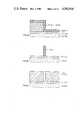
- FIGS. 1A to 1Fillustrate a basic method of the invention for negative lithography
- FIGS. 2A to 2Cillustrate a basic method of the invention for positive lithography
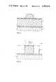
- FIG. 3is a three-layer structure for making a vertical profile of polymeric material
- FIG. 4shows the etching of a vertical polymeric material profile
- FIG. 5shows the deposition of silicon nitride or oxide on the horizontal and vertical surfaces of the polymeric material structure
- FIG. 6illustrates the making of silicon nitride or oxide walls by means of the etching
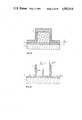
- FIG. 7Ashows the deposition of the actual mask material
- FIGS. 7B to 7Cshow variations of the mask material deposition method, and surface planarization
- FIG. 8illustrates removal of the silicon nitride or oxide walls embedded in the mask material
- FIG. 9illustrates opening of the mask down to the substrate by means of reactive ion etching
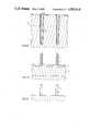
- FIG. 10shows etching deep trenches in the substrate using the mask
- FIG. 11shows filling these trenches by means of thermal oxidation
- FIG. 12shows etching the silicon dioxide off the surface, and subsequent reoxidation
- FIG. 13illustrates filling the trenches with synthetic material
- FIG. 14illustrates reversing the sidewall structure of FIG. 6 into a mask of a different material but with identical dimensions (positive lithography);
- FIG. 15shows the finished mask of the different material
- FIG. 16is a secondary electron microscope or scanning electron microscope graph (SEM) corresponds to FIG. 4 and shows a photoresist profile as an example of a polymeric material with vertical sidewalls;
- FIG. 17is an SEM corresponding to FIG. 5 and shows the silicon nitride-covered photoresist with vertical sidewalls;
- FIG. 18is a SEM corresponding to FIG. 6 and shows approximately 0.3 ⁇ m wide silicon nitride walls
- FIG. 19is a SEM corresponding to FIG. 7A and shows silicon nitride walls embedded in silicon dioxide deposited by means of cathode sputtering;
- FIG. 20is a SEM corresponding to FIG. 9 and depicts a silicon dioxide mask opened down to the silicon substrate;
- FIG. 21is a SEM corresponding to FIG. 10 and depicts the deep trenches in the silicon, with the silicon dioxide mask having already been removed;
- FIG. 22is a SEM corresponding to FIG. 12 and shows the trenches after having been filled by thermal oxidation.
- silicon dioxide or the like etching maskswith openings having a sub-micrometer width such as 0.2 ⁇ m wide openings with vertical sidewalls can be made.
- These etching masks usedcan be as an example for etching trenches in the slicon substrate with a width of 0.5 ⁇ m. The trenches are subsequently filled with dielectric material.
- the making an etching mask in a negative lithography processinvolves the following steps, following the basic method in accordance with FIGS. 1A to 1D:
- FIG. 1Aforming a vertical profile in a polymeric material layer by reactive ion etching, and plasma depositing silicon nitride or silicon dioxide (FIG. 1A);
- the trenchesare filled by thermal oxidation with silicon dioxide or with any other material.
- the silicon dioxide on the substrate surfaceis removed by reactive ion etching (FIG. 1F), and the silicon is reoxidized to form a layer thickness required for further processes.
- the reoxidationis performed following the hot processes. Prior to the filling with polyimide 13 (FIG. 13), a thermal oxidation is executed until the trench walls are covered with an approximately 15 nm thick oxide layer 11. This layer is sealed by depositing approximately 50 nm silicon nitride 12.
- FIG. 2Asilicon nitride or silicon dioxide
- FIG. 2Bconverting the mask according to FIG. 2B into a mask with identical dimensions, but made of a different material (FIG. 2C) by means of reactive in etching and stripping the walls of silicon nitride or silicon dioxide, respectively.
- FIGS. 3 to 9 and 14 and 15the lithography method as disclosed by the invention is described in general, and following that, with reference to a specific embodiment (FIGS. 10 to 13), the making of a deep dielectric isolation in a silicon semiconductor body is described.
- a layer 2 of dielectric materialis applied on a silicon semiconductor substrate in a conventional manner.
- Layer 2can consist of silicon dioxide produced by thermal oxidation at 925° C.
- Layer 2can also consist of a silicon dioxide and a silicon nitride layer, with the silicon dioxide layer being approximately 160 nm thick, and the silicon nitride layer approximately 100 nm.
- the silicon dioxide layeris usually produced by thermal oxidation, and the silicon nitride layer is deposited in a known manner out of an atmosphere containing silane, ammonia, and argon, at a temperature of approximately 1000° C.
- Layer 2can also consist of a layer sequence which will be referred to in detail in connection with FIG. 14. It is furthermore possible to apply the now following layers onto the surface of silicon substrate 1 directly.
- a polymere.g. a polyimide
- spin-coatingwhich is thermally stable up to approximately 400° to 450° C.
- the layer thickness of the polymeric materialdetermines the height of the silicon nitride or silicon dioxide walls which are made in further steps of the process.
- a series of known positive or negative resist materialsin the desired layer thickness, e.g. of approximately 2.0 ⁇ m.
- a positive resist materialwhich can e.g.
- resist layer 3is cured for forming the sidewall structure (FIG. 5).
- Resist layer 3 of the above specified materialcan e.g. be cured at a temperature of 210° C. for approximately 30 minutes.
- a silicon nitride layer 4approximately 100 nm thick is applied on resist layer 3.
- the silicon nitrideis plasma deposited out of an atmosphere containing silane, ammonia and argon at a pressure of approximately 1 mbar and an energy of 100 Watt (energy density 0.05 W/cm 2 ). The time required for this amounts to 3 to 4 minutes approximately.
- the deposition temperatureis 210° C., i.e. this is a so-called "cold process" which does not affect the material of layer 3.
- an approximately 1.0 ⁇ m thick resist layer 5is deposited on plasma silicon nitride layer 4.
- Layer 5can consist of the same resist material as layer 3. However, it can also consist of another highly radiation-sensitive photoresist, e.g. a methacrylate resist.
- a patternis generated by exposure and development.
- a resist mask 3 with edge angles of maximum steepnessis produced through reactive ion etching. For making the desired mask structure with edge angles of maximum steepness these resist sidewalls have to be as steep as possible.
- top resist layer 5As a mask, openings are etched into plasma nitride layer 4. Nitride layer 4 and polymeric or resist layer 3 therebeneath are etched by reactive ions. Plasma nitride layer 4 is etched in a reactor with carbon tetrafluoride under the following conditions:
- the plasma nitride etching rateis 30 nm/min. approximately.
- Layer 4 with the etched openingsis used as a mask for etching resist or polymeric layer 3.
- Layer 3is etched in a reactive ion etching process with oxygen, under the following conditions:
- the etching rate for a resistamounts to approximately 150 nm/min. under these conditions.
- reactive ion etchingis carried out at a very low oxygen pressure of approximately 2 to 5 ⁇ bar. If operations would take place at a higher oxygen pressure, lateral etching would increase which becomes apparent as lateral sub-etching of the silicon nitride mask.
- Plasma nitride and resist residuesare removed in a known manner by etching with buffered hydrofluoric acid.
- polymeric material 3 with vertical sidewallscan also be produced (no figures) in a modified image reversal process (German Pat. No. 25 29 054).
- This methodis inexpensive and not elaborate. It also results in structures with almost vertical sidewalls.
- a photosensitive layer containing a phenolformaldehyde resin, an o-quinonediazide, and a 1-hydroxyethyl-2-alkyl-imidazoline (Monazoline C)is applied on substrate 1, 2 of FIG. 3. This layer is exposed image-wise, and subsequently heated for 10 to 20 minutes to approximately 105° C.
- the nitride plasma depositionit is also possible to vapor deposit on the horizontal and vertical surfaces of the resist structure silicon dioxide or polysilicon at a low temperature.
- silicon nitride 6is plasma deposited out of an atmosphere containing silane, ammonia and argon at a pressure of 1 mbar and an energy density of 100 Watt, at a temperature of 210° C., in a layer thickness of approximately 400 nm. Silicon nitride 6 covers all horizontal and vertical surfaces of resist structure 3 and substrate 2 FIG. 17. Subsequently, the silicon nitride is removed from all horizontal surfaces by reactive ion etching in carbon tetrafluoride. For that purpose, etching takes place e.g. at a CF 4 flow of 30 cm 3 /min., a pressure of approximately 50 ⁇ bar and an energy density of 0.2 W/cm 2 .
- CF 4 etchingis interrupted when the entire silicon nitride has been removed from the horizontal surfaces.
- the etching end pointis determined by means of laser interference with 5 to 1-10% overetching.
- the process stepsare carried out analogously when the deposited material consists of silicon dioxide or polysilicon.
- resist 3is removed by reactive ion etching in an oxygen-containing atmosphere. Maintaining a particularly low oxygen pressure is not required for this step.
- any kind of material that can be deposited by spin-coatingcan be used for that purpose, e.g. a photoresist, polyimide or glass, or materials that can be sputtered on or vapor deposited, e.g. silicon dioxide, silicon nitride, magnesium oxide, polysilicon, aluminum oxide, metals etc.
- silicon dioxideis used as mask material, it can be deposited by means of cathode sputtering, or out of a silane or oxygen containing gas plasma, or by chemical vapor deposition out of a SiH 4 and oxygen, or SiH 2 Cl 2 and N 2 O containing atmosphere.
- the various deposition methodseach result in a different type of the silicon dioxide which covers plasma silicon nitride walls 6.
- silicon nitride walls 6are e.g. covered with silicon dioxide by means of cathode sputtering.
- This methodis preferred for the present invention.
- silicon dioxidestandard quartz
- a 0.5 ⁇ m thick silicon dioxide layerplanar quartz
- silicon dioxideis removed simultaneously with the deposition, so that structures with a surface topology are substantially planarized (FIG. 7A).
- FIGS. 7B and 7CFurther ways of covering silicon nitride walls 6 with silicon dioxide are depicted in FIGS. 7B and 7C.
- a 0.5 ⁇ m thick silicon dioxide layer 7ais chemically vapor deposited on the entire surface of the structure with silicon nitride walls 6.
- Chemical vapor depositionuses SiH 4 and O 2 at approximately 500° C., or SiH 2 Cl 2 and N 2 O at approximately 800° C., and atmospheric pressure or less.
- an approximately 1 ⁇ m thick silicon dioxide layeris deposited by means of cathode sputtering, with increased anode efficiency (planar quartz).
- silicon dioxide 7aWhile the vapor deposited silicon dioxide 7a uniformly grows around the walls, silicon dioxide 7b applied by cathode sputtering effects an increase of the silicon dioxide layer thickness, and a planarization of the regions over the silicon nitride walls 6 (FIG. 7B).
- silicon dioxide 7binstead of planar quartz, it is also possible to use a photoresist for planarization as layer 7b, and to cure it at 180° C.
- planarizing a structure in accordance with FIG. 7consists in depositing quartz under the usual cathode sputtering conditions, and to etch back until the peaks of silicon nitride walls 6 have been exposed (FIG. 7C).
- planarizationcan also be implemented in such a manner that instead of the quartz deposited by means of cathode sputtering, a photoresist is applied in a layer thickness of 2.0 ⁇ m, and cured at 180° C., and that subsequently the resist layer is partly removed until the peaks of the silicon nitride walls have been exposed (FIG. 7C).
- the silicon nitride walls embedded in silicon dioxide as a mask materialare removed in accordance with FIG. 8 by etching.
- the silicon dioxideis blanket removed in a layer thickness of approximately 0.3 ⁇ m by reactive ion etching with CF 4 .
- the silicon nitride wallsare removed by plasma etching in a system of the LFE Corporation and with carbon tetrafluoride, at a pressure of approximately 1.0 mbar, thus obtaining openings 8 with a width of 0.2 to 0.3 ⁇ m reaching down to the SiO 2 layer 2.
- the silicon nitride wallscan also be removed by wet etching. According to Fit.
- openings 8 of the silicon dioxide maskare extended by blanket reactive ion etching with CF 4 through layer 2 to silicon substrate 1. This step can also be carried out with CHF 3 gas because this ensures a better interruption of the etching process at the silicon substrate surface. During this etching, silicon dioxide is also removed from the mask surface. If the walls 6 defining height and width of mask openings 8 are made of silicon dioxide or polysilicon a photoresist has to be used for planarizing. With polysilicon walls it is also possible to employ quartz. Silicon dioxide or polysilicon walls 6 are removed by wet etching until layer 2 is reached which in this case consists of silicon nitride. FIG. 9 (FIG.
- the finished etching maskconsisting of silicon dioxide 7 which can be used for etching trenches in silicon substrate 1.
- the maskis approximately 0.6 to 1 ⁇ m thick, and has openings with practically vertical sidewalls and with a width of 0.2 to 0.3 ⁇ m.
- layer 2 of the above described figuresconsists of a double layer, i.e. of a layer 2a of the desired mask material, e.g. a photoresist, of polyimide, silicon dioxide, silicon nitride, polysilicon, metal, or combinations thereof with a thin dielectric layer 2b arranged on layer 2a and consisting of plasma nitride or oxide.
- a layer 2a of the desired mask materiale.g. a photoresist, of polyimide, silicon dioxide, silicon nitride, polysilicon, metal, or combinations thereof
- a thin dielectric layer 2barranged on layer 2a and consisting of plasma nitride or oxide.
- a sequence of layerse.g. silicon dioxide, polyimide, silicon dioxide can also be used.
- Sidewall structures 6with the sub-micrometer dimensions are made, as described above, by means of a polymeric material structure with vertical sidewalls.
- Dielectric layer 2bwhich consists of silicon dioxide if the sidewalls are made of plasma nitride, is removed by reactive ion etching in carbon tetrafluoride.
- Layer 2ais removed in the regions not covered by sidewalls 6 by reactive ion etching, too. If layer 2a consists of polymeric material, the reactive ion etching can be executed in an oxygen atmosphere.
- layer 2 of FIG. 14is made of a layer sequence of e.g. silicon dioxide, polyimide, silicon dioxide the top thin oxide layer, after the production of sub-micrometer mask 6, is etched in a CF 4 atmosphere, the polyimide in an oxygen atmosphere, and the silicon dioxide on the surface of the silicon substrate in a CF 4 atmosphere with reactive ions.
- the final mask of silicon dioxide on the silicon substrateis obtained.
- trenchesare etched in a silicon substrate.
- the trenchesare filled by thermal oxidation, or by the spin-coating of a synthetic material, e.g. polyimide.
- a silicon substratee.g. a semiconductor chip of P conductive material can be used.
- an N conductive layer with a maximum impurity concentration of 10 18 atoms/cm 3is epitaxially grown in a conventional method, at a temperature between 950° and 1170° C., and with a duration of approximately 17 minutes. While this layer is deposited, the N + conductive region diffuses out into this layer.
- Epitaxial layer 1(FIG. 3) is between 1 and 4 ⁇ m thick, corresponding with the other data of the integrated circuit. For the purposes of the present invention, an epitaxial layer 1 with a thickness of 2.35 ⁇ m is assumed, the epitaxial layer being 0.35 ⁇ m silicon are used up by oxidation during the implementation of the method as disclosed by the invention. Epitaxial layer 1, to give an example, can be applied using a device and a method as described in U.S. Pat. No. 3,424,629. In accordance with FIG. 3, a layer 2 of dielectric material is then deposited on epitaxial layer 1 in accordance with conventional methods.
- the forming of the vertical profile of polymeric materialis effected in a three-layer process (FIGS. 3 and 4), or in a modified mask reversal process.
- Plasma depositing of silicon nitride or silicon dioxide on all horizontal and vertical surfaces of the polymeric structure (FIG. 5)is performed at temperatures ⁇ 200° C. and ⁇ 400° C. This so-called low temperature process does not effect the polymeric structure materials.
- Silicon nitride or silicon dioxideis removed from all horizontal surfaces by reactive ion etching in an atmosphere containing CF 4 , and the removal of the polymeric material which results in silicon nitride or oxide walls is effected in an oxygen-containing atmosphere. Details of the method were discussed in connection with FIG. 6.
- the silicon nitride or dioxide wallsare converted in a mask reversal process in openings of a mask by depositing the mask material silicon dioxide over these walls, removing the silicon dioxide by etching until the peaks of the walls are exposed, and removing the silicon nitride or silicon dioxide walls by plasma etching.
- the method preferred within this embodiment for covering the silicon nitride walls with silicon dioxideis the method discussed in the specification with reference to FIG. 7A, where first approximately 1.3 ⁇ m silicon dioxide are deposited following the conventional method, and subsequently about 0.5 ⁇ m silicon dioxide are deposited in the planar method by means of cathode sputtering with increased anode efficiency.
- the silicon nitride wallsare removed after the exposure of the peaks by plasma etching with carbon tetrafluoride, and subsequently the openings of the silicon dioxide mask are extended by blanket reactive ion etching with carbon tetrafluoride to the silicon substrate. This process steps were discussed in the specification with reference to FIG. 8.
- FIG. 1Eshows the etching of the deep trenches in the silicon substrate
- FIG. 1Fdepicts the filling of the trenches with silicon dioxide or polyimide.
- the etching of the trenches in the silicon substrate, and their fillingwill be discussed in the following with reference to FIGS. 10 to 12, and the secondary electron microscope graphs FIGS. 21 and 22.
- FIG. 10depicts the making of trenches 9 in silicon substrate 1 by etching.
- the reactive ion etching performed for that purposeis carried out at the following conditions:
- etching medium10% chlorine, rest argon;
- etching siliconuses gas mixtures with a content of SF 6 , CL 2 and helium, or CCl 2 F 2 and O 2 or SiF 4 , Cl 2 , helium or argon.
- gas mixtures containing chlorine, fluorine, and/or oxygencan be used for the reactive ion etching of silicon.
- etching rate ratios of silicon to silicon dioxide of up to 20:1are obtained in a reactive ion etching device produced by Leybold.
- the above described etching processhas to be carried out twice, or a protective mask has to be used which covers the shallow trenches during the additional etching of the deep trenches.
- the remaining silicon dioxide etching maskis removed in a wet etching step with buffered hydrofluoric acid.
- FIG. 11depicts the filling of the trenches by thermal oxidation.
- This oxidationtakes place at approximately 1000° C., and is implemented as a dry-wet-dry oxidation, until approximately 0.5 ⁇ m silicon dioxide has formed in the trenches starting from either side of the trench wall, and on the surface a silicon dioxide of comparable layer thickness has formed.
- the oxidationcan also take place in the form of a high pressure oxidation at 850° C.
- the oxide in FIG. 11is removed by blanket reactive ion etching in CHF 3 with the etching being interrupted at the silicon surface. Then, the silicon is reoxidized to a layer thickness of approximately 160 nm (FIG. 12).
- the following processcan be applied (FIG. 13):
- dielectric isolationswith a width of approximately 0.5 to 1.0 ⁇ m.
- Deep and shallow isolationscan be made simultaneously, e.g. a subcollector isolation with a depth of 4 to 5 ⁇ m and a base isolation with a depth of 1 ⁇ m.
- the minimum distance between two isolationsis approximately 1.5 to 2.0 ⁇ m.
- the interface between the isolation and the silicon substratehas a low charge level owing to the thermal oxidation.
- Filling the trenches with polyimide instead of by thermal oxidationis particularly advantageous because defects were observed in the silicon when the trenches were completely filled by thermal oxidation. When the filling takes place by vapor deposition of oxide, such defects can be substantially avoided.
- the method describedis a planar process, therefore the forming of the undesired "bird's heads" is avoided.
- subcollector, base and emittercan directly be adjacent to the isolation; the forming of the undesired "bird's beak" is avoided, too.
- trenchesare etched subsequently to the diffusion of subcollector, base and emitter.
- the quality of the devices made in accordance with the method as disclosed by the inventionis improved owing to the lower capacity caused by the diffusions directly adjacent to the isolations and owing to shorter electric conductive paths.
- the general method as disclosed by the invention for making structures with dimensions in the sub-micrometer rangeuses, instead of dielectric materials, polymeric materials to define structures with horizontal and vertical surfaces, e.g. a photoresist or polyimide.
- the polymeric materialscan be deposited inexpensively and easily by spin-coating. They can be vertically etched in an excellent manner, particularly using the above described three layer process, with reactive oxygen ions.
- the polymeric layer determining position and height of the maskcan be applied with a much higher layer thickness than e.g. dielectric materials. For that reason, thicker masks can be made than with other processes. With masks having a thickness of e.g. up to 3 ⁇ m up to 6 ⁇ m deep trenches can be etched in a silicon substrate.
- the sidewall structures of silicon dioxide or silicon nitrideare made in a plasma deposition process that can be carried out at temperatures of ⁇ 200° C., and which represents a so-called low temperature process so that there is no damage of the polymer structures.
- the process temperatures that are low compared with prior artfurthermore permit a more universal applicability of the method.
- the method as disclosed by the inventionis suitable not only for making deep dielectric isolations with a trench width in the sub-micrometer range; further possible uses are e.g. making field effect transistors with a channel length in the sub-micrometer range, or making lateral, bipolar PNP transistors with a base width in the sub-micrometer range.
Landscapes
- Engineering & Computer Science (AREA)
- Manufacturing & Machinery (AREA)
- Physics & Mathematics (AREA)
- Condensed Matter Physics & Semiconductors (AREA)
- General Physics & Mathematics (AREA)
- Computer Hardware Design (AREA)
- Microelectronics & Electronic Packaging (AREA)
- Power Engineering (AREA)
- Inorganic Chemistry (AREA)
- Chemical & Material Sciences (AREA)
- Drying Of Semiconductors (AREA)
- Element Separation (AREA)
- ing And Chemical Polishing (AREA)
Abstract
Description
1. Technical Field
The invention relates to a method of making structures with dimensions in the sub-micrometer range, and to the implementation of this method to make a deep dielectric isolation with sub-micrometer width in a silicon body.
2. Background Art
A number of methods are known to increase the integration density of integrated circuits. Considerable increases of integration density have recently been achieved mainly by decreasing photolithographic defect densities. By using electron and X-ray exposure methods instead of the hitherto used light radiation, a progress was made in the direction of a higher optical resolution. There were furthermore efforts to reach very narrow line widths in the 1 μm range and less by extending conventional lithographic processes, avoiding the cost-intensive techniques of electron and X-ray lithography. With the technique of plasma or reactive ion etching for etching metals, semi-conductive and dielectric materials further developments took place in the direction of very narrow line widths, and consequently toward an increased integration density.
A number of publications and patents describe the so-called sidewall technology by means of which structures in the sub-micrometer range can be made. In IEEE Electron Device Letters, Vol. EDL-2, No. 1, January 1981, pp. 4 to 6, a method is described where vertical (anisotropic) dry etching methods are applied for making MOSFETs which are defined by an edge and have dimensions in the sub-micrometer range. The technology described permits the production of physical channel lengths of the MOSFETs in the 0.1 to 0.15 μm range.
U.S. Pat. No. 4,358,340 describes a method of making sub-micrometer devices, but without using the sub-micrometer lithography, where a conductive thin film with dimensions in the sub-micrometer range is deposited across a vertical step between adjacent surfaces of an isolation, and subsequently vertically etched until there only remains that part of the conductive film which is adjacent the vertical step. The remaining isolation not covered by the conductor is removed, thus obtaining a gate of an MOS field effect transistor with a width in the sub-micrometer range which equals the layer thickness of the originally applied thin film.
U.S. Pat. No. 4,209,349 describes a method of forming very small mask openings for making semiconductor circuit arrangements. According to this method, first insulator regions are formed on a substrate so that substantially horizontal as well as substantially vertical surfaces are obtained. A second insulator layer is applied thereon of a material different from that of the first insulator layer, and it is subjected to a reactive ion etching process in such a manner that the horizontal regions of the second insulator layer are removed, with merely very narrow regions of this layer remaining on the vertical surface regions of the first insulator layer, and the respective regions of the substrate, respectively. Subsequently, the exposed substrate regions are thermally oxidized, and for finally forming the desired mask openings the regions of the second insulating layer there are removed. By means of this method, minimum dimensions smaller than those of hitherto applied photolithographic methods are to be obtained.
In the process of this U.S. patent, the first insulator layer (silicon dioxide) determines the position and thickness of the mask (column 2, line 62). All openings in the insulator layer are made by standard photolithography and etching techniques (column 3, line 21) according to which no vertical sidewalls can be made. In the method as disclosed by the invention however a polymeric layer determines position and thickness of the mask. In the method of the U.S. patent, only hot processes are applied, e.g. a thermal oxidation at 970° C. (column 4, line 65), and the chemical vapor deposition of silicon nitride at approximately 1000° C. (column 5, line 69), whereas in the method as disclosed by the invention so-called cold processes at less than 300° C. are performed permitting a more universal application of the method. With the method of the U.S. patent, masks with a layer thickness of less than 0.5 μm can be made which are not suitable as masks e.g. for etching deep trenches. With the method as disclosed by the invention however masks with a thickness of 2 to 3 μm can be made that can be used for etching 4 to 5 μm deep trenches in a silicon substrate. From thermal oxidation (column 4, line 64 of the U.S. patent) there results an asymmetrical mask with the bird's beak problem being involved which originates from the forming of a non-planar silicon dioxide on the trench surface, so that the mask cannot be used for trench etching also for that reason. The mask made in accordance with the invention has strictly vertical sidewalls and is of a symmetrical structure.
A feature common to all hitherto known methods is that for making structures with vertical sidewalls and dimensions in the sub-micrometer range materials as polysilicon, silicon nitride or silicon dioxide are used which are all deposited at higher temperatures. None of the publications describes the use of polymeric materials for the purpose.
Using the method as disclosed by the invention is particularly advantageous in the production of deep dielectric isolations with sub-micrometer width in a semiconductor body. In the following, the various isolation methods will be briefly referred to. One of the known isolation methods for isolating against each other various active and/or passive elements in integrated circuit structures is the so-called junction isolation, where isolation regions are formed in the semiconductor regions are surrounded with oppositely doped semiconductor regions. The thus formed semiconductor junctions form reverse-operated diodes effecting isolation. Another known isolation method is the so-called dielectric isolation. There, the semiconductor regions to be isolated are surrounded with a dielectric isolation region. In an embodiment thereof, trenches are made in silicon in which the isolation regions are subsequently made. During the etching of the trenches, the remaining semiconductor substrate surface is protected by a protective layer consisting of a silicon dioxide-silicon nitride sandwich structure. Following the forming of the trenches, the silicon semiconductor substrate is conventionally oxidized, so that the silicon in the trench region is oxidized and the resulting silicon dioxide fills the trenches. In the conventional thermal oxidation for filling the trenches with oxide however undesired structures appear at the trench edges which are called "bird's beak". The term bird's beak refers to the forming of a non-planar silicon dioxide on the trench surface which is caused by lateral oxidation underneath the silicon dioxide layer and which effects an elevation of the silicon dioxide/silicon nitride structure at the trench edges. The direct bordering of diffusions at the isolation which represents an essential advantage of the originally planned dielectric isolation is thus no longer possible.
An alternative to the embedded oxide isolation is the deep dielectric isolation comprising the forming of rectangular trenches through reactive ion etching methods, and the filling of these trenches to form the isolation for the various silicon regions of the substrate. This method, too, presents some important disadvantages, e.g. no thermal oxide can be used for filling the trenches but only an oxide which is chemically vapor deposited out of a silane and oxygen-containing phase, or polysilicon. Filling of the trenches with oxide through chemical vapor deposition can in turn cause a poor oxide quality or a seam in the middle of the trenches which can influence the continuity of the metallic conductor on the surface, and finally cause conductivity defects. During the various subsequent temperature processes, the chemically vapor deposited oxide does not have the same thermal expansion coefficient as silicon, and causes tensions round the trenches at process temperatures around 1000° C. Furthermore, chemically vapor deposited oxide is difficult to planarize.
It is therefore desirable to have a method available according to which deep dielectric isolations with sub-micrometer width can be made which do not have the above specified disadvantages. It is furthermore intended to provide dielectric isolations with a width of approximately 1 μm and a depth of approximately 5 μm in silicon semiconductor substrates.
The invention as characterized in the claims achieves the object of providing an improved lithography method with reduced line widths down into the sub-micrometer range. A further object of the invention is the application of this method to make deep dielectric isolations with widths in the sub-micrometer range.
To summarize, the method as disclosed by the invention provides a structure of polymeric material with vertical sidewalls, the latter serving to make sidewall structures of silicon dioxide or nitride with dimensions in the sub-micrometer range. These sidewall structures can be used as masks directly. For the negative lithography, another layer is alternatively applied over the sidewall structures, which is partly removed until the peaks of the sidewall structures are exposed. Subsequently the sidewall structures themselves are removed. The resulting opening can then be used as a mask for a plurality of processes for making integrated circuits. The invention also comprises the application of the method of making deep dielectric isolations with sub-micrometer width in a silicon semiconductor body.
The drawings show the following:
FIGS. 1A to 1F illustrate a basic method of the invention for negative lithography;
FIGS. 2A to 2C illustrate a basic method of the invention for positive lithography;
FIG. 3 is a three-layer structure for making a vertical profile of polymeric material;
FIG. 4 shows the etching of a vertical polymeric material profile;
FIG. 5 shows the deposition of silicon nitride or oxide on the horizontal and vertical surfaces of the polymeric material structure;
FIG. 6 illustrates the making of silicon nitride or oxide walls by means of the etching;
FIG. 7A shows the deposition of the actual mask material;
FIGS. 7B to 7C show variations of the mask material deposition method, and surface planarization;
FIG. 8 illustrates removal of the silicon nitride or oxide walls embedded in the mask material;
FIG. 9 illustrates opening of the mask down to the substrate by means of reactive ion etching;
FIG. 10 shows etching deep trenches in the substrate using the mask;
FIG. 11 shows filling these trenches by means of thermal oxidation;
FIG. 12 shows etching the silicon dioxide off the surface, and subsequent reoxidation;
FIG. 13 illustrates filling the trenches with synthetic material;
FIG. 14 illustrates reversing the sidewall structure of FIG. 6 into a mask of a different material but with identical dimensions (positive lithography);
FIG. 15 shows the finished mask of the different material;
FIG. 16 is a secondary electron microscope or scanning electron microscope graph (SEM) corresponds to FIG. 4 and shows a photoresist profile as an example of a polymeric material with vertical sidewalls;
FIG. 17 is an SEM corresponding to FIG. 5 and shows the silicon nitride-covered photoresist with vertical sidewalls;
FIG. 18 is a SEM corresponding to FIG. 6 and shows approximately 0.3 μm wide silicon nitride walls;
FIG. 19 is a SEM corresponding to FIG. 7A and shows silicon nitride walls embedded in silicon dioxide deposited by means of cathode sputtering;
FIG. 20 is a SEM corresponding to FIG. 9 and depicts a silicon dioxide mask opened down to the silicon substrate;
FIG. 21 is a SEM corresponding to FIG. 10 and depicts the deep trenches in the silicon, with the silicon dioxide mask having already been removed;
FIG. 22 is a SEM corresponding to FIG. 12 and shows the trenches after having been filled by thermal oxidation.
With the method as disclosed by the invention and according to a preferred embodiment, silicon dioxide or the like etching masks with openings having a sub-micrometer width such as 0.2 μm wide openings with vertical sidewalls can be made. These etching masks used can be as an example for etching trenches in the slicon substrate with a width of 0.5 μm. The trenches are subsequently filled with dielectric material.
The making an etching mask in a negative lithography process involves the following steps, following the basic method in accordance with FIGS. 1A to 1D:
forming a vertical profile in a polymeric material layer by reactive ion etching, and plasma depositing silicon nitride or silicon dioxide (FIG. 1A);
removing silicon nitride or silicon dioxide from all horizontal surfaces by reactive ion etching, and removing the polymeric material, thus obtaining silicon nitride or silicon dioxide walls (FIG. 1B);
converting the silicon nitride or silicon dioxide walls into openings of a mask in a reversal process by depositing the mask material over the silicon nitride or silicon dioxide walls, removing the mask material by etching until the peaks of the silicon nitride or silicon dioxide walls are exposed, and removing the silicon nitride or silicon dioxide walls by plasma etching or wet etching (FIG. 1C);
opening the mask down to the substrate (FIG. 1D).
Using the thus made mask trenches are etched into the silicon substrate by reactive ion etching, and the mask material is removed (FIG. 1E). Subsequently, the trenches are filled by thermal oxidation with silicon dioxide or with any other material. The silicon dioxide on the substrate surface is removed by reactive ion etching (FIG. 1F), and the silicon is reoxidized to form a layer thickness required for further processes. If the trenches are filled with polyimide, the reoxidation is performed following the hot processes. Prior to the filling with polyimide 13 (FIG. 13), a thermal oxidation is executed until the trench walls are covered with an approximately 15 nm thick oxide layer 11. This layer is sealed by depositing approximately 50nm silicon nitride 12.
For making a mask of a different mask material, but with the same dimensions the following steps have to be performed in accordance with FIGS. 2A to 2C:
as described above, forming a vertical profile in a polymeric material layer, and plasma depositing silicon nitride or silicon dioxide (FIG. 2A);
removing silicon nitride or silicon dioxide from all horizontal surfaces, and removing the polymeric material, thus obtaining silicon nitride or silicon dioxide walls (FIG. 2B);
converting the mask according to FIG. 2B into a mask with identical dimensions, but made of a different material (FIG. 2C) by means of reactive in etching and stripping the walls of silicon nitride or silicon dioxide, respectively.
With reference to FIGS. 3 to 9 and 14 and 15, the lithography method as disclosed by the invention is described in general, and following that, with reference to a specific embodiment (FIGS. 10 to 13), the making of a deep dielectric isolation in a silicon semiconductor body is described.
According to FIG. 3, alayer 2 of dielectric material is applied on a silicon semiconductor substrate in a conventional manner.Layer 2, to give an example, can consist of silicon dioxide produced by thermal oxidation at 925°C. Layer 2 can also consist of a silicon dioxide and a silicon nitride layer, with the silicon dioxide layer being approximately 160 nm thick, and the silicon nitride layer approximately 100 nm. The silicon dioxide layer is usually produced by thermal oxidation, and the silicon nitride layer is deposited in a known manner out of an atmosphere containing silane, ammonia, and argon, at a temperature of approximately 1000° C. Instead of the double layer of silicon dioxide-silicon nitride, it is also possible to apply a double layer of silicon dioxide and polysilicon, or polysilicon and silicon dioxide, respectively.Layer 2 can also consist of a layer sequence which will be referred to in detail in connection with FIG. 14. It is furthermore possible to apply the now following layers onto the surface ofsilicon substrate 1 directly.
For making a structure of polymeric material with vertical sidewalls, a polymer, e.g. a polyimide, is applied by spin-coating which is thermally stable up to approximately 400° to 450° C. It should be noted that the layer thickness of the polymeric material determines the height of the silicon nitride or silicon dioxide walls which are made in further steps of the process. It is also possible to apply as polymeric materials a series of known positive or negative resist materials in the desired layer thickness, e.g. of approximately 2.0 μm. A positive resist material which can e.g. be used is a resist produced by Shipley commercially available under the trade designation 1350J, and consisting of a phenolformaldehyde resin and a naphthoquinone diazide sensitizer which is identified as 3, 4-dihydroxybenzophenone-4-[naphthoquinone(1,2)-diazide(2)]sulfonate. At a temperature which is equal to, or higher than the deposition temperature ofmaterial 6, resistlayer 3 is cured for forming the sidewall structure (FIG. 5). Resistlayer 3 of the above specified material can e.g. be cured at a temperature of 210° C. for approximately 30 minutes. As an etching barrier for reactive ion etching with oxygen, a silicon nitride layer 4 approximately 100 nm thick is applied on resistlayer 3. The silicon nitride is plasma deposited out of an atmosphere containing silane, ammonia and argon at a pressure of approximately 1 mbar and an energy of 100 Watt (energy density 0.05 W/cm2). The time required for this amounts to 3 to 4 minutes approximately. It should be noted that the deposition temperature is 210° C., i.e. this is a so-called "cold process" which does not affect the material oflayer 3. In the same manner, it is possible to plasma deposit instead of silicon nitride layer 4 a silicon dioxide layer, or a polysilicon layer on resistlayer 3. In the present case, an approximately 1.0 μm thick resistlayer 5 is deposited on plasma silicon nitride layer 4.Layer 5 can consist of the same resist material aslayer 3. However, it can also consist of another highly radiation-sensitive photoresist, e.g. a methacrylate resist. Inlayer 5, a pattern is generated by exposure and development. Subsequently, as depicted in FIG. 4 and FIG. 16, a resistmask 3 with edge angles of maximum steepness is produced through reactive ion etching. For making the desired mask structure with edge angles of maximum steepness these resist sidewalls have to be as steep as possible.
Using the top resistlayer 5 as a mask, openings are etched into plasma nitride layer 4. Nitride layer 4 and polymeric or resistlayer 3 therebeneath are etched by reactive ions. Plasma nitride layer 4 is etched in a reactor with carbon tetrafluoride under the following conditions:
CF4 flow: 30 cm3 /min.;
pressure: 50 μbar;
energy density: 0.2 Watt/cm2.
Under these conditions, the plasma nitride etching rate is 30 nm/min. approximately.
Layer 4 with the etched openings is used as a mask for etching resist orpolymeric layer 3.
O2 flow: 10-100 cm3 /min;
pressure: 2-3 μbar;
energy density: 0.2 Watt/cm2.
The etching rate for a resist amounts to approximately 150 nm/min. under these conditions. In order to arrive at resist sidewalls of maximum steepness, reactive ion etching is carried out at a very low oxygen pressure of approximately 2 to 5 μbar. If operations would take place at a higher oxygen pressure, lateral etching would increase which becomes apparent as lateral sub-etching of the silicon nitride mask. Plasma nitride and resist residues are removed in a known manner by etching with buffered hydrofluoric acid. In connection with the above described three-layer process for making resist sidewalls of maximum steepness, reference is also made to the PCT application WO 80/00639, Western Electric, U.S. priority Sept. 11, 1978 (Ser. No. 941,369).
The structure ofpolymeric material 3 with vertical sidewalls can also be produced (no figures) in a modified image reversal process (German Pat. No. 25 29 054). This method is inexpensive and not elaborate. It also results in structures with almost vertical sidewalls. In detail, for making a resist image that is negative relative to the original, a photosensitive layer containing a phenolformaldehyde resin, an o-quinonediazide, and a 1-hydroxyethyl-2-alkyl-imidazoline (Monazoline C) is applied onsubstrate
Resiststructure 3 onsubstrate silicon nitride 6 on the horizontal and vertical surfaces of resiststructure 3 and ofsubstrate 2, as well as the making of plasma nitride walls by removing the nitride from all horizontal surfaces through reactive ion etching, and equally through reactive ion etching the removing of resist 3. Instead of the nitride plasma deposition, it is also possible to vapor deposit on the horizontal and vertical surfaces of the resist structure silicon dioxide or polysilicon at a low temperature.
In accordance with FIG. 5,silicon nitride 6 is plasma deposited out of an atmosphere containing silane, ammonia and argon at a pressure of 1 mbar and an energy density of 100 Watt, at a temperature of 210° C., in a layer thickness of approximately 400 nm.Silicon nitride 6 covers all horizontal and vertical surfaces of resiststructure 3 andsubstrate 2 FIG. 17. Subsequently, the silicon nitride is removed from all horizontal surfaces by reactive ion etching in carbon tetrafluoride. For that purpose, etching takes place e.g. at a CF4 flow of 30 cm3 /min., a pressure of approximately 50 μbar and an energy density of 0.2 W/cm2. CF4 etching is interrupted when the entire silicon nitride has been removed from the horizontal surfaces. The etching end point is determined by means of laser interference with 5 to 1-10% overetching. The process steps are carried out analogously when the deposited material consists of silicon dioxide or polysilicon. As described above, resist 3 is removed by reactive ion etching in an oxygen-containing atmosphere. Maintaining a particularly low oxygen pressure is not required for this step.
According to FIG. 6 (FIG. 18), approximately nm thicksilicon nitride walls 6 remain after the two previously mentioned etching steps.
In negative lithography, there now follows the deposition of the desired mask material (FIG. 7A). Any kind of material that can be deposited by spin-coating can be used for that purpose, e.g. a photoresist, polyimide or glass, or materials that can be sputtered on or vapor deposited, e.g. silicon dioxide, silicon nitride, magnesium oxide, polysilicon, aluminum oxide, metals etc. If silicon dioxide is used as mask material, it can be deposited by means of cathode sputtering, or out of a silane or oxygen containing gas plasma, or by chemical vapor deposition out of a SiH4 and oxygen, or SiH2 Cl2 and N2 O containing atmosphere. The various deposition methods each result in a different type of the silicon dioxide which covers plasmasilicon nitride walls 6.
According to FIG. 7A (FIG. 19),silicon nitride walls 6 are e.g. covered with silicon dioxide by means of cathode sputtering. This method is preferred for the present invention. First, approximately 1.3 μm silicon dioxide (standard quartz) are applied by cathode sputtering by means of a standard process. Subsequently, a 0.5 μm thick silicon dioxide layer (planar quartz) is deposited following the planar process by means of cathode sputtering with increased anode efficiency. Following this method, silicon dioxide is removed simultaneously with the deposition, so that structures with a surface topology are substantially planarized (FIG. 7A).
Further ways of coveringsilicon nitride walls 6 with silicon dioxide are depicted in FIGS. 7B and 7C. Following FIG. 7B, a 0.5 μm thick silicon dioxide layer 7a is chemically vapor deposited on the entire surface of the structure withsilicon nitride walls 6. Chemical vapor deposition uses SiH4 and O2 at approximately 500° C., or SiH2 Cl2 and N2 O at approximately 800° C., and atmospheric pressure or less. Subsequently, an approximately 1 μm thick silicon dioxide layer is deposited by means of cathode sputtering, with increased anode efficiency (planar quartz). While the vapor deposited silicon dioxide 7a uniformly grows around the walls, silicon dioxide 7b applied by cathode sputtering effects an increase of the silicon dioxide layer thickness, and a planarization of the regions over the silicon nitride walls 6 (FIG. 7B). Instead of planar quartz, it is also possible to use a photoresist for planarization as layer 7b, and to cure it at 180° C.
Another way of planarizing a structure in accordance with FIG. 7 consists in depositing quartz under the usual cathode sputtering conditions, and to etch back until the peaks ofsilicon nitride walls 6 have been exposed (FIG. 7C). As already indicated in connection with the planarization in accordance with FIG. 7B, such planarization can also be implemented in such a manner that instead of the quartz deposited by means of cathode sputtering, a photoresist is applied in a layer thickness of 2.0 μm, and cured at 180° C., and that subsequently the resist layer is partly removed until the peaks of the silicon nitride walls have been exposed (FIG. 7C).
In the subsequent process step, the silicon nitride walls embedded in silicon dioxide as a mask material are removed in accordance with FIG. 8 by etching. First, the silicon dioxide is blanket removed in a layer thickness of approximately 0.3 μm by reactive ion etching with CF4. Subsequently, the silicon nitride walls are removed by plasma etching in a system of the LFE Corporation and with carbon tetrafluoride, at a pressure of approximately 1.0 mbar, thus obtainingopenings 8 with a width of 0.2 to 0.3 μm reaching down to the SiO2 layer 2. The silicon nitride walls can also be removed by wet etching. According to Fit. 9,openings 8 of the silicon dioxide mask are extended by blanket reactive ion etching with CF4 throughlayer 2 tosilicon substrate 1. This step can also be carried out with CHF3 gas because this ensures a better interruption of the etching process at the silicon substrate surface. During this etching, silicon dioxide is also removed from the mask surface. If thewalls 6 defining height and width ofmask openings 8 are made of silicon dioxide or polysilicon a photoresist has to be used for planarizing. With polysilicon walls it is also possible to employ quartz. Silicon dioxide orpolysilicon walls 6 are removed by wet etching untillayer 2 is reached which in this case consists of silicon nitride. FIG. 9 (FIG. 20) represents the finished etching mask consisting ofsilicon dioxide 7 which can be used for etching trenches insilicon substrate 1. The mask is approximately 0.6 to 1 μm thick, and has openings with practically vertical sidewalls and with a width of 0.2 to 0.3 μm.
Up to now, a method of making a mask using the sidewall technology has been described, resulting in a mask negative to the original mask pattern. Basing on FIG. 6, a method will now be described with reference to FIGS. 14 and 15 according to which sidewalls 6 can be converted into a mask positive to the original pattern, with identical dimensions but made of a different material. According to FIG. 14,layer 2 of the above described figures consists of a double layer, i.e. of a layer 2a of the desired mask material, e.g. a photoresist, of polyimide, silicon dioxide, silicon nitride, polysilicon, metal, or combinations thereof with a thin dielectric layer 2b arranged on layer 2a and consisting of plasma nitride or oxide. Instead oflayer 2, a sequence of layers, e.g. silicon dioxide, polyimide, silicon dioxide can also be used.Sidewall structures 6 with the sub-micrometer dimensions are made, as described above, by means of a polymeric material structure with vertical sidewalls. Dielectric layer 2b which consists of silicon dioxide if the sidewalls are made of plasma nitride, is removed by reactive ion etching in carbon tetrafluoride. Layer 2a is removed in the regions not covered bysidewalls 6 by reactive ion etching, too. If layer 2a consists of polymeric material, the reactive ion etching can be executed in an oxygen atmosphere. Subsequently,sidewall structures 6 and the remaining silicon dioxide of layer 2b are removed by plasma etching as described above or wet etching. The result is a positive mask structure with the dimensions of the plasma nitride columns in accordance with FIG. 6 which however are made of the material of layer 2a (FIGS. 14 and 15).
Iflayer 2 of FIG. 14 is made of a layer sequence of e.g. silicon dioxide, polyimide, silicon dioxide the top thin oxide layer, after the production ofsub-micrometer mask 6, is etched in a CF4 atmosphere, the polyimide in an oxygen atmosphere, and the silicon dioxide on the surface of the silicon substrate in a CF4 atmosphere with reactive ions. By plasma etching in oxygen, or by dissolving the middle polyimide layer of the etched structures, the final mask of silicon dioxide on the silicon substrate is obtained.
In the following, a specific application of the above described method is discussed, where in a mask reversal process the structures of FIG. 6 are used for making asilicon dioxide mask 7.
Using this mask, trenches are etched in a silicon substrate. The trenches are filled by thermal oxidation, or by the spin-coating of a synthetic material, e.g. polyimide. As a silicon substrate, e.g. a semiconductor chip of P conductive material can be used. On this substrate with a resistivity of 10 Ω-cm in which an N+ conductive region has been made (not shown) an N conductive layer with a maximum impurity concentration of 1018 atoms/cm3 is epitaxially grown in a conventional method, at a temperature between 950° and 1170° C., and with a duration of approximately 17 minutes. While this layer is deposited, the N+ conductive region diffuses out into this layer. Epitaxial layer 1 (FIG. 3) is between 1 and 4 μm thick, corresponding with the other data of the integrated circuit. For the purposes of the present invention, anepitaxial layer 1 with a thickness of 2.35 μm is assumed, the epitaxial layer being 0.35 μm silicon are used up by oxidation during the implementation of the method as disclosed by the invention.Epitaxial layer 1, to give an example, can be applied using a device and a method as described in U.S. Pat. No. 3,424,629. In accordance with FIG. 3, alayer 2 of dielectric material is then deposited onepitaxial layer 1 in accordance with conventional methods.
Following the basic method shown in FIGS. 1A to 1F, and the specific description, the following procedures can be used for making the trenches and for filling the trenches.
Forming a vertical profile of polymeric material by reactive ion etching, and plasma depositing of silicon nitride or silicon dioxide. As specified above in detail, the forming of the vertical profile of polymeric material is effected in a three-layer process (FIGS. 3 and 4), or in a modified mask reversal process. Plasma depositing of silicon nitride or silicon dioxide on all horizontal and vertical surfaces of the polymeric structure (FIG. 5) is performed at temperatures ≧200° C. and ≧400° C. This so-called low temperature process does not effect the polymeric structure materials.
Silicon nitride or silicon dioxide is removed from all horizontal surfaces by reactive ion etching in an atmosphere containing CF4, and the removal of the polymeric material which results in silicon nitride or oxide walls is effected in an oxygen-containing atmosphere. Details of the method were discussed in connection with FIG. 6.
The silicon nitride or dioxide walls are converted in a mask reversal process in openings of a mask by depositing the mask material silicon dioxide over these walls, removing the silicon dioxide by etching until the peaks of the walls are exposed, and removing the silicon nitride or silicon dioxide walls by plasma etching. The method preferred within this embodiment for covering the silicon nitride walls with silicon dioxide is the method discussed in the specification with reference to FIG. 7A, where first approximately 1.3 μm silicon dioxide are deposited following the conventional method, and subsequently about 0.5 μm silicon dioxide are deposited in the planar method by means of cathode sputtering with increased anode efficiency. The silicon nitride walls are removed after the exposure of the peaks by plasma etching with carbon tetrafluoride, and subsequently the openings of the silicon dioxide mask are extended by blanket reactive ion etching with carbon tetrafluoride to the silicon substrate. This process steps were discussed in the specification with reference to FIG. 8.
In the process survey, FIG. 1E shows the etching of the deep trenches in the silicon substrate, and FIG. 1F depicts the filling of the trenches with silicon dioxide or polyimide. The etching of the trenches in the silicon substrate, and their filling will be discussed in the following with reference to FIGS. 10 to 12, and the secondary electron microscope graphs FIGS. 21 and 22.
FIG. 10 (FIG. 21) depicts the making oftrenches 9 insilicon substrate 1 by etching. The reactive ion etching performed for that purpose is carried out at the following conditions:
etching medium: 10% chlorine, rest argon;
flow: 30 cm3 /min.;
pressure: 15 mbar;
energy density: 0.2 Watt/cm2.
Other methods for etching silicon use gas mixtures with a content of SF6, CL2 and helium, or CCl2 F2 and O2 or SiF4, Cl2, helium or argon. Generally, gas mixtures containing chlorine, fluorine, and/or oxygen can be used for the reactive ion etching of silicon. In a system with 10% Cl2 in argon, etching rate ratios of silicon to silicon dioxide of up to 20:1 are obtained in a reactive ion etching device produced by Leybold. If deep and shallow trenches are to be etched simultaneously, the above described etching process has to be carried out twice, or a protective mask has to be used which covers the shallow trenches during the additional etching of the deep trenches. According to FIG. 10, the remaining silicon dioxide etching mask is removed in a wet etching step with buffered hydrofluoric acid.
FIG. 11 depicts the filling of the trenches by thermal oxidation. This oxidation takes place at approximately 1000° C., and is implemented as a dry-wet-dry oxidation, until approximately 0.5 μm silicon dioxide has formed in the trenches starting from either side of the trench wall, and on the surface a silicon dioxide of comparable layer thickness has formed. The oxidation can also take place in the form of a high pressure oxidation at 850° C. In order to obtain anoxide layer 10 on silicon substrate surface 1 (FIG. 12, FIG. 22) in a layer thickness necessary for subsequent etching and diffusion processes, the oxide in FIG. 11 is removed by blanket reactive ion etching in CHF3 with the etching being interrupted at the silicon surface. Then, the silicon is reoxidized to a layer thickness of approximately 160 nm (FIG. 12). Instead of the filling of the trenches by thermal oxidation, the following process can be applied (FIG. 13):
(a) thermal oxidation to produce approximately 25 nm silicon dioxide 11;
(b) vapor depositing approximately 50nm silicon nitride 12;
(c) completely filling the trenches withpolyimide 13 which is spun-on in a known manner.
In the following, the essential features and advantages of the method as disclosed by the invention when applied to making deep dielectric isolations with sub-micrometer widths will be repeated:
It is possible to make dielectric isolations with a width of approximately 0.5 to 1.0 μm.
Deep and shallow isolations can be made simultaneously, e.g. a subcollector isolation with a depth of 4 to 5 μm and a base isolation with a depth of 1 μm.
The minimum distance between two isolations is approximately 1.5 to 2.0 μm.
The interface between the isolation and the silicon substrate has a low charge level owing to the thermal oxidation.
Filling the trenches with polyimide instead of by thermal oxidation is particularly advantageous because defects were observed in the silicon when the trenches were completely filled by thermal oxidation. When the filling takes place by vapor deposition of oxide, such defects can be substantially avoided.
The method described is a planar process, therefore the forming of the undesired "bird's heads" is avoided.
The diffusions of subcollector, base and emitter can directly be adjacent to the isolation; the forming of the undesired "bird's beak" is avoided, too. When filling with polyimide takes place, the trenches are etched subsequently to the diffusion of subcollector, base and emitter.
The quality of the devices made in accordance with the method as disclosed by the invention is improved owing to the lower capacity caused by the diffusions directly adjacent to the isolations and owing to shorter electric conductive paths.
There results a higher integration density from the lower isolation width and the diffusions directly adjacent to the diffusions.
The general method as disclosed by the invention for making structures with dimensions in the sub-micrometer range uses, instead of dielectric materials, polymeric materials to define structures with horizontal and vertical surfaces, e.g. a photoresist or polyimide. The polymeric materials can be deposited inexpensively and easily by spin-coating. They can be vertically etched in an excellent manner, particularly using the above described three layer process, with reactive oxygen ions. The polymeric layer determining position and height of the mask can be applied with a much higher layer thickness than e.g. dielectric materials. For that reason, thicker masks can be made than with other processes. With masks having a thickness of e.g. up to 3 μm up to 6 μm deep trenches can be etched in a silicon substrate. The sidewall structures of silicon dioxide or silicon nitride are made in a plasma deposition process that can be carried out at temperatures of ≧200° C., and which represents a so-called low temperature process so that there is no damage of the polymer structures. The process temperatures that are low compared with prior art furthermore permit a more universal applicability of the method. The method as disclosed by the invention is suitable not only for making deep dielectric isolations with a trench width in the sub-micrometer range; further possible uses are e.g. making field effect transistors with a channel length in the sub-micrometer range, or making lateral, bipolar PNP transistors with a base width in the sub-micrometer range.
Claims (22)
1. Method for fabricating sub-micrometer dimensioned structures using a polymeric layer comprising:
providing a body to form said structures;
depositing said polymeric layer upon said body;
removing portions of said polymeric layer where the edges of the formed openings are at locations where said sub-micrometer dimensioned structures are desired;
forming a sub-micrometer dimensioned sidewall structure on the said edges of the polymeric layer of substantially the same width as the desired said sub-micrometer dimensioned structures and at a temperature which is less than a temperature which would adversely affect said polymeric layer;
removing the remaining said polymeric layer; and
using the said sidewall structure as the mask to form the sub-micrometer structures in said body.
2. Method for fabricating sub-micrometer dimensioned structures using a polymeric layer comprising:
providing a body to form said structures;
depositing said polymeric layer upon said body;
removing portions of said polymeric layer where the edges of the formed openings are at locations where said sub-micrometer dimensioned structures are desired;
forming a sub-micrometer dimensioned sidewall structure on the said edges of the polymeric layer of substantially the same width as the desired and sub-micrometer dimensioned structures and at a temperature which is less than a temperature which would adversely affect said polymeric layer;
removing the remaining said polymeric layer;
depositing a mask material layer over said sidewall layer;
removing said sidewall layer; and
using as a mask the said maks material layer having the openings left by said sidewall structure for making sub-micrometer structures in said body.
3. Method of making structures with dimensions in the sub-micrometer range in a layer arranged on a silicon substrate comprising:
forming an isolating layer upon said silicon substrate;
forming upon said isolating layer a polymeric layer having substantially horizontal surfaces and substantially vertical surfaces;
forming upon the vertical surfaces of said polymeric layer a sub-micrometer dimensioned sidewall layer at a temperature less than that temperature which would adversely effect said polymeric layer;
removing said polymeric layer in such a manner that said sidewall layer remains upon the isolating layer; and
that in the case of positive lithography the said sidewall layer directly serves as a mask for forming structures in the said substrate with dimensions in the submicrometer range.
4. Method of making structures with dimensions in the sub-micrometer range in a layer arranged on a silicon substrate comprising:
forming an isolating layer upon said silicon substrate;
forming upon said isolating layer a polymeric layer having substantially horizontal surfaces and substantially vertical surfaces;
forming upon the vertical surfaces of said polymeric layer a sub-micrometer dimensioned sidewall layer at a temperature less than that temperature which would adversely effect said polymeric layer;
removing said polymeric layer in such a manner that sidewall layer remains upon the isolating layer;
that in the case of negative lithography the said sidewall layer is embedded into a desired mask material; and
removing said sidewall layer embedded in the mask material by etching which results in mask openings having dimensions in the submicrometer range which serve as a mask for forming structures in said substrate.
5. The method as in claim 3 or 4 wherein the polymeric layer is formed by applying the polymeric layer directly upon the said isolating layer, a layer of plasma deposited silicon nitride upon the polymeric layer and a top layer of a photoresist upon said silicon nitride layer;
forming the desired pattern in the top photoresist layer and transferring the pattern by anisotropic reactive ion etching into the said plasma silicon nitride layer and into the polymeric layer respectively.
6. The method as in claim 5 characterized in that the polymeric layer is a positive photoresist and is between about 1.0 μm and 2.0 μm thick, that the said plasma silicon nitride layer is between about 0.2 μm and 0.5 μm thick, and that the top said photoresist layer is a highly sensitive photoresist and is between 0.5 μm to 1.5 μm thick.
7. The method as in claim 5 wherein the said pattern is transferred from the said top layer by reactive ion etching with CF4 into the said plasma silicon nitride layer, and by reactive ion etching with oxygen at a pressure of less than 5 μbar into the said polymeric layer.
8. The method as in claim 3 wherein said isolating layer is a silicon dioxide layer and is produced by means of thermal oxidation.
9. The method as in claim 3 or 4 wherein said sidewall layer is silicon nitride deposited upon the said horizontal and substantially vertical surfaces of the said polymeric layer and the exposed said isolating layer by plasma deposition out of an atmosphere containing silane, ammonia and argon, at a pressure of approximately 1 μbar, an energy of about 100 Watt (energy density of 0.05 Watt/cm2) and a temperature of about 210° C. or less.
10. The method as in claim 9 wherein the said horizontal regions of the silicon nitride layer are removed by reactive ion etching with CF4, and the said polymeric layer removed by reactive ion etching with oxygen.
11. The method as claimed in claim 3 wherein the said isolating layer is composed of two component layers and is removed in the regions not covered by the said sidewall layer by means of reactive ion etching, and that subsequently the said sidewall layer and the remains of the said isolating layer therebeneath are etched off, with a mask with the dimensions of the original pattern, but consisting of the material of the top of said component layers.
12. The method as claimed in claim 4 wherein said mask material is composed of polymeric material.
13. The method as claimed in claim 4 wherein said mask material is deposited by means of a 2 stage sputtering method with a first thicker layer being applied under the standard conditions, and a second, thinner layer being deposited with increased anode efficiency to achieve an improved surface planarity.
14. The method as claimed in claim 4 wherein said mask material is a silicon dioxide layer, and a first portion of said silicon dioxide layer is chemically vapor deposited uniformly over the said sidewall layer walls, and that subsequently by means of sputtering a second thicker silicon dioxide layer is deposited over said first portion with increased anode efficiency to increase the silicon dioxide layer thickness, and to achieve an improved surface planarity.
15. The method as claimed in claim 12 wherein said polymeric material is a photoresist material layer which is spun-on and etched back for surface planarization.
16. The method as claimed in claim 4 wherein said mask material layer is blanket removed by reactive ion etching until the peaks of the said sidewall layer are exposed, and then removing said sidewall layer by etching to form openings in said mask material layer extending to the surface of the said silicon substrate.
17. The method as claimed in claim 16 wherein the said mask material is silicon dioxide, the said sidewall layer is silicon nitride, and the sidewall layer is removed by etching with CF4 to the surface of the silicon substrate.
18. The method for making a deep dielectric isolation with submicrometer width within a silicon body comprising:
forming an isolating layer upon said silicon substrate;
forming upon said isolating layer a polymeric layer having substantially horizontal surfaces and substantially vertical surfaces;
forming upon the vertical surfaces of said polymeric layer a sub-micrometer dimensioned sidewall layer at a temperature less than that temperature which would adversely effect said polymeric layer;
removing said polymeric layer in such a manner that sidewall layer remains upon the isolating layer;
that in the case of negative lithography the said sidewall layer is embedded into a desired mask material;
removing said sidewall layer embedded in the mask material by etching which results in mask openings having dimensions in the submicrometer range which serve as a mask for forming structures in said substrate;
etching trenches through said mask openings into the silicon substrate by reactive ion etching; and
filling said trenches with dielectric material.
19. The method as claimed in claim 18 wherein the said trenches in the silicon substrate are made by reactive ion etching in a CCl2 F2 /oxygen ambient.
20. The method as claimed in claim 19 wherein deep and shallow trenches are made in said silicon substrate by covering the designated shallow trenches during an additional etching step which forms the deep trenches.
21. The method as claimed in any one of claim 18 wherein the said trenches are filled by a thermal oxidation to produce thin silicon dioxide layer, a vapor deposition to produce slightly thicker silicon nitride layer and the said trenches are then completely filled with polyimide.
22. The method as claimed in claim 18 wherein after the said trenches are filled by thermal oxidation, the silicon dioxide is removed from the silicon substrate surface by blanket reactive ion etching with CHF3, and that subsequently the silicon substrate is reoxidized to an silicon dioxide layer thickness required for the subsequent processes.
Applications Claiming Priority (3)
| Application Number | Priority Date | Filing Date | Title |
|---|---|---|---|
| DE19823242113DE3242113A1 (en) | 1982-11-13 | 1982-11-13 | METHOD FOR PRODUCING A THIN DIELECTRIC INSULATION IN A SILICON SEMICONDUCTOR BODY |
| DE3242113 | 1982-11-13 | ||
| EP83109945.2 | 1983-10-05 |
Publications (1)
| Publication Number | Publication Date |
|---|---|
| US4502914Atrue US4502914A (en) | 1985-03-05 |
Family
ID=6178117
Family Applications (1)
| Application Number | Title | Priority Date | Filing Date |
|---|---|---|---|
| US06/546,612Expired - LifetimeUS4502914A (en) | 1982-11-13 | 1983-10-28 | Method of making structures with dimensions in the sub-micrometer range |
Country Status (4)
| Country | Link |
|---|---|
| US (1) | US4502914A (en) |
| EP (1) | EP0111086B1 (en) |
| JP (1) | JPS59107518A (en) |
| DE (2) | DE3242113A1 (en) |
Cited By (146)
| Publication number | Priority date | Publication date | Assignee | Title |
|---|---|---|---|---|
| US4568601A (en)* | 1984-10-19 | 1986-02-04 | International Business Machines Corporation | Use of radiation sensitive polymerizable oligomers to produce polyimide negative resists and planarized dielectric components for semiconductor structures |
| US4586980A (en)* | 1984-02-20 | 1986-05-06 | Canon Kabushiki Kaisha | Pattern forming method |
| US4596070A (en)* | 1984-07-13 | 1986-06-24 | Texas Instruments Incorporated | Interdigitated IMPATT devices |
| US4599136A (en)* | 1984-10-03 | 1986-07-08 | International Business Machines Corporation | Method for preparation of semiconductor structures and devices which utilize polymeric dielectric materials |
| US4631803A (en)* | 1985-02-14 | 1986-12-30 | Texas Instruments Incorporated | Method of fabricating defect free trench isolation devices |
| US4661204A (en)* | 1985-10-25 | 1987-04-28 | Tandem Computers Inc. | Method for forming vertical interconnects in polyimide insulating layers |
| US4663832A (en)* | 1984-06-29 | 1987-05-12 | International Business Machines Corporation | Method for improving the planarity and passivation in a semiconductor isolation trench arrangement |
| US4689871A (en)* | 1985-09-24 | 1987-09-01 | Texas Instruments Incorporated | Method of forming vertically integrated current source |
| EP0238690A1 (en)* | 1986-03-27 | 1987-09-30 | International Business Machines Corporation | Process for forming sidewalls |
| US4707218A (en)* | 1986-10-28 | 1987-11-17 | International Business Machines Corporation | Lithographic image size reduction |
| US4753901A (en)* | 1985-11-15 | 1988-06-28 | Ncr Corporation | Two mask technique for planarized trench oxide isolation of integrated devices |
| US4755478A (en)* | 1987-08-13 | 1988-07-05 | International Business Machines Corporation | Method of forming metal-strapped polysilicon gate electrode for FET device |
| US4776922A (en)* | 1987-10-30 | 1988-10-11 | International Business Machines Corporation | Formation of variable-width sidewall structures |
| US4796070A (en)* | 1987-01-15 | 1989-01-03 | General Electric Company | Lateral charge control semiconductor device and method of fabrication |
| US4799990A (en)* | 1987-04-30 | 1989-01-24 | Ibm Corporation | Method of self-aligning a trench isolation structure to an implanted well region |
| US4838991A (en)* | 1987-10-30 | 1989-06-13 | International Business Machines Corporation | Process for defining organic sidewall structures |
| US4839305A (en)* | 1988-06-28 | 1989-06-13 | Texas Instruments Incorporated | Method of making single polysilicon self-aligned transistor |
| US4869781A (en)* | 1987-10-30 | 1989-09-26 | International Business Machines Corporation | Method for fabricating a semiconductor integrated circuit structure having a submicrometer length device element |
| US4886763A (en)* | 1987-08-21 | 1989-12-12 | Oki Electric Industry Co., Ltd. | Device isolation by etching trench in dielectric on substrate and epitaxially filling the trench |
| US4931137A (en)* | 1986-11-28 | 1990-06-05 | Commissariat A L'energie Atomique | Process for producing mutually spaced conductor elements on a substrate |
| US4941026A (en)* | 1986-12-05 | 1990-07-10 | General Electric Company | Semiconductor devices exhibiting minimum on-resistance |
| US4980317A (en)* | 1988-04-19 | 1990-12-25 | International Business Machines Corporation | Method of producing integrated semiconductor structures comprising field-effect transistors with channel lengths in the submicron range using a three-layer resist system |
| US5047117A (en)* | 1990-09-26 | 1991-09-10 | Micron Technology, Inc. | Method of forming a narrow self-aligned, annular opening in a masking layer |
| US5055383A (en)* | 1988-11-17 | 1991-10-08 | International Business Machines Corporation | Process for making masks with structures in the submicron range |
| USH986H (en) | 1989-06-09 | 1991-11-05 | International Business Machines Corporation | Field effect-transistor with asymmetrical structure |
| US5082795A (en)* | 1986-12-05 | 1992-01-21 | General Electric Company | Method of fabricating a field effect semiconductor device having a self-aligned structure |
| US5084130A (en)* | 1985-09-21 | 1992-01-28 | Semiconductor Energy Laboratory Co., Ltd. | Method for depositing material on depressions |
| US5110760A (en)* | 1990-09-28 | 1992-05-05 | The United States Of America As Represented By The Secretary Of The Navy | Method of nanometer lithography |
| US5118384A (en)* | 1990-04-03 | 1992-06-02 | International Business Machines Corporation | Reactive ion etching buffer mask |
| US5118383A (en)* | 1990-02-01 | 1992-06-02 | Siemens Aktiengesellschaft | Method for producing trench structures in silicon substrates for vlsi semiconductor circuits |
| US5202272A (en)* | 1991-03-25 | 1993-04-13 | International Business Machines Corporation | Field effect transistor formed with deep-submicron gate |
| US5236853A (en)* | 1992-02-21 | 1993-08-17 | United Microelectronics Corporation | Self-aligned double density polysilicon lines for ROM and EPROM |
| US5254218A (en)* | 1992-04-22 | 1993-10-19 | Micron Technology, Inc. | Masking layer having narrow isolated spacings and the method for forming said masking layer and the method for forming narrow isolated trenches defined by said masking layer |
| US5298466A (en)* | 1987-08-07 | 1994-03-29 | Cobrain N.V. | Method and apparatus for dry anisotropically etching a substrate |
| US5378646A (en)* | 1994-07-07 | 1995-01-03 | United Microelectronics Corporation | Process for producing closely spaced conductive lines for integrated circuits |
| US5429988A (en)* | 1994-06-13 | 1995-07-04 | United Microelectronics Corporation | Process for producing high density conductive lines |
| US5459099A (en)* | 1990-09-28 | 1995-10-17 | The United States Of America As Represented By The Secretary Of The Navy | Method of fabricating sub-half-micron trenches and holes |
| US5462767A (en)* | 1985-09-21 | 1995-10-31 | Semiconductor Energy Laboratory Co., Ltd. | CVD of conformal coatings over a depression using alkylmetal precursors |
| US5510286A (en)* | 1994-07-14 | 1996-04-23 | Hyundai Electronics Industries Co., Ltd. | Method for forming narrow contact holes of a semiconductor device |
| US5573837A (en)* | 1992-04-22 | 1996-11-12 | Micron Technology, Inc. | Masking layer having narrow isolated spacings and the method for forming said masking layer and the method for forming narrow isolated trenches defined by said masking layer |
| US5595941A (en)* | 1994-06-01 | 1997-01-21 | Mitsubishi Denki Kabushiki Kaisha | Method of forming fine patterns |
| EP0755067A1 (en)* | 1995-07-17 | 1997-01-22 | Siemens Aktiengesellschaft | Method of fabrication for sublithographic etching masks |
| US5612255A (en)* | 1993-12-21 | 1997-03-18 | International Business Machines Corporation | One dimensional silicon quantum wire devices and the method of manufacture thereof |
| US5618383A (en)* | 1994-03-30 | 1997-04-08 | Texas Instruments Incorporated | Narrow lateral dimensioned microelectronic structures and method of forming the same |
| WO1997032342A1 (en)* | 1996-03-01 | 1997-09-04 | Ace Memory, Inc. | High capacity stacked dram device and process |
| US5665997A (en)* | 1994-03-31 | 1997-09-09 | Texas Instruments Incorporated | Grated landing area to eliminate sticking of micro-mechanical devices |
| US5667632A (en)* | 1995-11-13 | 1997-09-16 | Motorola, Inc. | Method of defining a line width |
| US5702976A (en)* | 1995-10-24 | 1997-12-30 | Micron Technology, Inc. | Shallow trench isolation using low dielectric constant insulator |
| US5711851A (en)* | 1996-07-12 | 1998-01-27 | Micron Technology, Inc. | Process for improving the performance of a temperature-sensitive etch process |
| US5767017A (en)* | 1995-12-21 | 1998-06-16 | International Business Machines Corporation | Selective removal of vertical portions of a film |
| US5928967A (en)* | 1996-06-10 | 1999-07-27 | International Business Machines Corporation | Selective oxide-to-nitride etch process using C4 F8 /CO/Ar |
| US5952246A (en)* | 1993-11-03 | 1999-09-14 | Advanced Micro Devices, Inc. | Nitride selective, anisotropic Cl2 /He etch process |
| US6104038A (en)* | 1995-06-07 | 2000-08-15 | Micron Technology, Inc. | Method for fabricating an array of ultra-small pores for chalcogenide memory cells |
| US6127708A (en)* | 1996-04-25 | 2000-10-03 | Nec Corporation | Semiconductor device having an intervening region between channel stopper and diffusion region |
| US6136211A (en)* | 1997-11-12 | 2000-10-24 | Applied Materials, Inc. | Self-cleaning etch process |
| US6139647A (en)* | 1995-12-21 | 2000-10-31 | International Business Machines Corporation | Selective removal of vertical portions of a film |
| US6139483A (en)* | 1993-07-27 | 2000-10-31 | Texas Instruments Incorporated | Method of forming lateral resonant tunneling devices |
| US20010002046A1 (en)* | 1997-05-09 | 2001-05-31 | Reinberg Alan R. | Small electrode for a chalcogenide switching device and method for fabricating same |
| US6291137B1 (en)* | 1999-01-20 | 2001-09-18 | Advanced Micro Devices, Inc. | Sidewall formation for sidewall patterning of sub 100 nm structures |
| US6322714B1 (en) | 1997-11-12 | 2001-11-27 | Applied Materials Inc. | Process for etching silicon-containing material on substrates |
| US6323101B1 (en) | 1998-09-03 | 2001-11-27 | Micron Technology, Inc. | Semiconductor processing methods, methods of forming silicon dioxide methods of forming trench isolation regions, and methods of forming interlevel dielectric layers |
| US6362057B1 (en) | 1999-10-26 | 2002-03-26 | Motorola, Inc. | Method for forming a semiconductor device |
| US6383951B1 (en) | 1998-09-03 | 2002-05-07 | Micron Technology, Inc. | Low dielectric constant material for integrated circuit fabrication |
| US6392913B1 (en) | 1996-06-18 | 2002-05-21 | Micron Technology, Inc. | Method of forming a polysilicon diode and devices incorporating such diode |
| US6423475B1 (en)* | 1999-03-11 | 2002-07-23 | Advanced Micro Devices, Inc. | Sidewall formation for sidewall patterning of sub 100 nm structures |
| US6429449B1 (en) | 1995-06-07 | 2002-08-06 | Micron Technology, Inc. | Three-dimensional container diode for use with multi-state material in a non-volatile memory cell |
| US6440837B1 (en) | 2000-07-14 | 2002-08-27 | Micron Technology, Inc. | Method of forming a contact structure in a semiconductor device |
| US6444531B1 (en) | 2000-08-24 | 2002-09-03 | Infineon Technologies Ag | Disposable spacer technology for device tailoring |
| US6455394B1 (en) | 1998-03-13 | 2002-09-24 | Micron Technology, Inc. | Method for trench isolation by selective deposition of low temperature oxide films |
| US20020179896A1 (en)* | 1995-06-07 | 2002-12-05 | Harshfield Steven T. | Method and apparatus for forming an integrated circuit electrode having a reduced contact area |
| US6527968B1 (en) | 2000-03-27 | 2003-03-04 | Applied Materials Inc. | Two-stage self-cleaning silicon etch process |
| US6531391B2 (en) | 1996-07-22 | 2003-03-11 | Micron Technology, Inc. | Method of fabricating a conductive path in a semiconductor device |
| US6534368B2 (en) | 1997-01-28 | 2003-03-18 | Micron Technology, Inc. | Integrated circuit memory cell having a small active area and method of forming same |
| US6540928B1 (en) | 1999-09-10 | 2003-04-01 | Unaxis Usa Inc. | Magnetic pole fabrication process and device |
| US6547975B1 (en) | 1999-10-29 | 2003-04-15 | Unaxis Usa Inc. | Magnetic pole fabrication process and device |
| US6563156B2 (en) | 2001-03-15 | 2003-05-13 | Micron Technology, Inc. | Memory elements and methods for making same |
| US6670713B2 (en) | 1996-02-23 | 2003-12-30 | Micron Technology, Inc. | Method for forming conductors in semiconductor devices |
| US20040017989A1 (en)* | 2002-07-23 | 2004-01-29 | So Daniel W. | Fabricating sub-resolution structures in planar lightwave devices |
| US6781212B1 (en) | 1998-08-31 | 2004-08-24 | Micron Technology, Inc | Selectively doped trench device isolation |
| US6797188B1 (en) | 1997-11-12 | 2004-09-28 | Meihua Shen | Self-cleaning process for etching silicon-containing material |
| US6852242B2 (en) | 2001-02-23 | 2005-02-08 | Zhi-Wen Sun | Cleaning of multicompositional etchant residues |
| US6862798B2 (en) | 2002-01-18 | 2005-03-08 | Hitachi Global Storage Technologies Netherlands B.V. | Method of making a narrow pole tip by ion beam deposition |
| US6872322B1 (en) | 1997-11-12 | 2005-03-29 | Applied Materials, Inc. | Multiple stage process for cleaning process chambers |
| US6905800B1 (en) | 2000-11-21 | 2005-06-14 | Stephen Yuen | Etching a substrate in a process zone |
| DE102004027425A1 (en)* | 2004-06-04 | 2005-09-29 | Infineon Technologies Ag | Forming a trench in a substrate surface layer, comprises covering a primary layer with a mask, applying a second layer to the mask structure, etching, and polishing |
| US20050277249A1 (en)* | 2004-05-26 | 2005-12-15 | Werner Juengling | Methods for forming semiconductor structures |
| US20060046200A1 (en)* | 2004-09-01 | 2006-03-02 | Abatchev Mirzafer K | Mask material conversion |
| US20060046484A1 (en)* | 2004-09-02 | 2006-03-02 | Abatchev Mirzafer K | Method for integrated circuit fabrication using pitch multiplication |
| US20060046201A1 (en)* | 2004-09-02 | 2006-03-02 | Sandhu Gurtej S | Method to align mask patterns |
| US20060046407A1 (en)* | 2004-09-01 | 2006-03-02 | Werner Juengling | DRAM cells with vertical transistors |
| US20060046422A1 (en)* | 2004-08-31 | 2006-03-02 | Micron Technology, Inc. | Methods for increasing photo alignment margins |
| US20060211260A1 (en)* | 2005-03-15 | 2006-09-21 | Luan Tran | Pitch reduced patterns relative to photolithography features |
| US20060216923A1 (en)* | 2005-03-28 | 2006-09-28 | Tran Luan C | Integrated circuit fabrication |
| US20060263699A1 (en)* | 2005-05-23 | 2006-11-23 | Mirzafer Abatchev | Methods for forming arrays of a small, closely spaced features |
| US20060273456A1 (en)* | 2005-06-02 | 2006-12-07 | Micron Technology, Inc., A Corporation | Multiple spacer steps for pitch multiplication |
| US20060278911A1 (en)* | 2005-06-14 | 2006-12-14 | Eppich Anton P | Relaxed-pitch method of aligning active area to digit line |
| US20060281266A1 (en)* | 2005-06-09 | 2006-12-14 | Wells David H | Method and apparatus for adjusting feature size and position |
| US20060289919A1 (en)* | 2005-06-24 | 2006-12-28 | Werner Juengling | Two-sided surround access transistor for a 4.5F2 DRAM cell |
| US20070018223A1 (en)* | 2005-07-25 | 2007-01-25 | Micron Technology Inc. | Dram including a vertical surround gate transistor |
| US20070018206A1 (en)* | 2005-07-06 | 2007-01-25 | Leonard Forbes | Surround gate access transistors with grown ultra-thin bodies |
| US20070026672A1 (en)* | 2005-07-29 | 2007-02-01 | Micron Technology, Inc. | Pitch doubled circuit layout |
| US20070048674A1 (en)* | 2005-09-01 | 2007-03-01 | Wells David H | Methods for forming arrays of small, closely spaced features |
| US20070045712A1 (en)* | 2005-09-01 | 2007-03-01 | Haller Gordon A | Memory cell layout and process flow |
| US20070049032A1 (en)* | 2005-09-01 | 2007-03-01 | Mirzafer Abatchev | Protective coating for planarization |
| US20070049030A1 (en)* | 2005-09-01 | 2007-03-01 | Sandhu Gurtej S | Pitch multiplication spacers and methods of forming the same |
| US20070049035A1 (en)* | 2005-08-31 | 2007-03-01 | Tran Luan C | Method of forming pitch multipled contacts |
| US20070049040A1 (en)* | 2005-03-15 | 2007-03-01 | Micron Technology, Inc., A Corporation | Multiple deposition for integration of spacers in pitch multiplication process |
| US20070050748A1 (en)* | 2005-08-30 | 2007-03-01 | Micron Technology, Inc., A Corporation | Method and algorithm for random half pitched interconnect layout with constant spacing |
| US20070051997A1 (en)* | 2005-08-31 | 2007-03-08 | Gordon Haller | Semiconductor memory device |
| US20070105357A1 (en)* | 2005-09-01 | 2007-05-10 | Micron Technology, Inc. | Silicided recessed silicon |
| US20070159617A1 (en)* | 2006-01-11 | 2007-07-12 | Mackey Jeffrey L | Photolithographic systems and methods for producing sub-diffraction-limited features |
| US20070190713A1 (en)* | 2006-02-16 | 2007-08-16 | International Business Machines Corporation | CMOS Gate Structures Fabricated By Selective Oxidation |
| US20070205438A1 (en)* | 2006-03-02 | 2007-09-06 | Werner Juengling | Masking process for simultaneously patterning separate regions |
| US20070205443A1 (en)* | 2006-03-02 | 2007-09-06 | Werner Juengling | Vertical gated access transistor |
| US20070215960A1 (en)* | 2004-03-19 | 2007-09-20 | The Regents Of The University Of California | Methods for Fabrication of Positional and Compositionally Controlled Nanostructures on Substrate |
| US20070238308A1 (en)* | 2006-04-07 | 2007-10-11 | Ardavan Niroomand | Simplified pitch doubling process flow |
| US20070249170A1 (en)* | 2006-04-25 | 2007-10-25 | David Kewley | Process for improving critical dimension uniformity of integrated circuit arrays |
| US20070261016A1 (en)* | 2006-04-24 | 2007-11-08 | Sandhu Gurtej S | Masking techniques and templates for dense semiconductor fabrication |
| US20070281219A1 (en)* | 2006-06-01 | 2007-12-06 | Sandhu Gurtej S | Masking techniques and contact imprint reticles for dense semiconductor fabrication |
| US20080057724A1 (en)* | 2006-08-31 | 2008-03-06 | Mark Kiehlbauch | Selective etch chemistries for forming high aspect ratio features and associated structures |
| US20080057692A1 (en)* | 2006-08-30 | 2008-03-06 | Wells David H | Single spacer process for multiplying pitch by a factor greater than two and related intermediate IC structures |
| US20080070165A1 (en)* | 2006-09-14 | 2008-03-20 | Mark Fischer | Efficient pitch multiplication process |
| US20080085612A1 (en)* | 2006-10-05 | 2008-04-10 | Micron Technology, Inc. | Method to deposit conformal low temperature SiO2 |
| US20080149593A1 (en)* | 2005-08-25 | 2008-06-26 | Micron Technology, Inc. | Multiple deposition for integration of spacers in pitch multiplication process |
| US20080299753A1 (en)* | 2005-09-01 | 2008-12-04 | Figura Thomas A | Peripheral Gate Stacks and Recessed Array Gates |
| US20080299774A1 (en)* | 2007-06-04 | 2008-12-04 | Micron Technology, Inc. | Pitch multiplication using self-assembling materials |
| US20080318169A1 (en)* | 2007-06-21 | 2008-12-25 | Shuichi Taniguchi | Pattern forming method |
| US20090017628A1 (en)* | 2007-07-10 | 2009-01-15 | Advanced Micro Devices, Inc. | Spacer lithography |
| US20090035665A1 (en)* | 2007-07-31 | 2009-02-05 | Micron Technology, Inc. | Process of semiconductor fabrication with mask overlay on pitch multiplied features and associated structures |
| US20090139540A1 (en)* | 2007-11-30 | 2009-06-04 | Applied Materials, Inc. | Repairing surface defects and cleaning residues from plasma chamber components |
| US20090152645A1 (en)* | 2007-12-18 | 2009-06-18 | Micron Technology, Inc. | Methods for isolating portions of a loop of pitch-multiplied material and related structures |
| US20090286936A1 (en)* | 2005-04-25 | 2009-11-19 | Tokyo Ohka Kogyo Co., Ltd. | Composition for formation of mold |
| US7659208B2 (en) | 2007-12-06 | 2010-02-09 | Micron Technology, Inc | Method for forming high density patterns |
| US20100062579A1 (en)* | 2008-09-11 | 2010-03-11 | Micron Technology, Inc. | Self-aligned trench formation |
| US20100130016A1 (en)* | 2008-11-24 | 2010-05-27 | Micron Technology, Inc. | Methods of forming a masking pattern for integrated circuits |
| US7737039B2 (en) | 2007-11-01 | 2010-06-15 | Micron Technology, Inc. | Spacer process for on pitch contacts and related structures |
| US7759197B2 (en) | 2005-09-01 | 2010-07-20 | Micron Technology, Inc. | Method of forming isolated features using pitch multiplication |
| US20110121383A1 (en)* | 2005-05-13 | 2011-05-26 | Micron Technology, Inc. | Memory array with surrounding gate access transistors and capacitors with global and staggered local bit lines |
| US20110165744A1 (en)* | 2005-05-13 | 2011-07-07 | Micron Technology | Memory array with ultra-thin etched pillar surround gate access transistors and buried data/bit lines |
| US8030218B2 (en) | 2008-03-21 | 2011-10-04 | Micron Technology, Inc. | Method for selectively modifying spacing between pitch multiplied structures |
| US8076208B2 (en) | 2008-07-03 | 2011-12-13 | Micron Technology, Inc. | Method for forming transistor with high breakdown voltage using pitch multiplication technique |
| US8114573B2 (en) | 2006-06-02 | 2012-02-14 | Micron Technology, Inc. | Topography based patterning |
| US20140370684A1 (en)* | 2013-06-14 | 2014-12-18 | Micron Technology, Inc. | Methods for forming sub-resolution features in semiconductor devices |
| US9312064B1 (en) | 2015-03-02 | 2016-04-12 | Western Digital (Fremont), Llc | Method to fabricate a magnetic head including ion milling of read gap using dual layer hard mask |
| US9406331B1 (en) | 2013-06-17 | 2016-08-02 | Western Digital (Fremont), Llc | Method for making ultra-narrow read sensor and read transducer device resulting therefrom |
| US9673049B2 (en) | 2015-03-09 | 2017-06-06 | United Microelectronics Corp. | Manufacturing method of patterned structure of semiconductor device |
Families Citing this family (13)
| Publication number | Priority date | Publication date | Assignee | Title |
|---|---|---|---|---|
| US4534826A (en)* | 1983-12-29 | 1985-08-13 | Ibm Corporation | Trench etch process for dielectric isolation |
| US4654119A (en)* | 1985-11-18 | 1987-03-31 | International Business Machines Corporation | Method for making submicron mask openings using sidewall and lift-off techniques |
| EP0226517A3 (en)* | 1985-12-18 | 1989-10-18 | Fairchild Semiconductor Corporation | Method for isolating regions of different impurity concentrations in a semiconductor substrate |
| US4726879A (en)* | 1986-09-08 | 1988-02-23 | International Business Machines Corporation | RIE process for etching silicon isolation trenches and polycides with vertical surfaces |
| FR2610141B1 (en)* | 1987-01-26 | 1990-01-19 | Commissariat Energie Atomique | CMOS INTEGRATED CIRCUIT AND METHOD FOR MANUFACTURING ELECTRICAL ISOLATION AREAS IN THIS CIRCUIT |
| JPH0626202B2 (en)* | 1987-10-30 | 1994-04-06 | インターナシヨナル・ビジネス・マシーンズ・コーポレーシヨン | Patterning method |
| JPH01119028A (en)* | 1987-10-30 | 1989-05-11 | Nec Corp | Manufacture of semiconductor device |
| JPH0817169B2 (en)* | 1988-03-11 | 1996-02-21 | 株式会社日立製作所 | Plasma etching method |
| JP2550728B2 (en)* | 1989-12-06 | 1996-11-06 | 三菱電機株式会社 | Method for manufacturing semiconductor device |
| DE4236609A1 (en)* | 1992-10-29 | 1994-05-05 | Siemens Ag | Method for forming a structure in the surface of a substrate - with an auxiliary structure laterally bounding an initial masking structure, followed by selective removal of masking structure using the auxiliary structure as an etching mask |
| DE19643185C2 (en)* | 1996-10-18 | 1998-09-10 | Siemens Ag | Dual-gate memory cell and method for producing a non-volatile memory cell |
| JP2006310350A (en)* | 2005-04-26 | 2006-11-09 | Ishikawajima Harima Heavy Ind Co Ltd | Method for forming isolation region between elements |
| JP2011233922A (en)* | 2011-07-20 | 2011-11-17 | Ihi Corp | Method of forming inter-device isolating region |
Citations (6)
| Publication number | Priority date | Publication date | Assignee | Title |
|---|---|---|---|---|
| US4042726A (en)* | 1974-09-11 | 1977-08-16 | Hitachi, Ltd. | Selective oxidation method |
| US4313782A (en)* | 1979-11-14 | 1982-02-02 | Rca Corporation | Method of manufacturing submicron channel transistors |
| US4331708A (en)* | 1980-11-04 | 1982-05-25 | Texas Instruments Incorporated | Method of fabricating narrow deep grooves in silicon |
| US4334348A (en)* | 1980-07-21 | 1982-06-15 | Data General Corporation | Retro-etch process for forming gate electrodes of MOS integrated circuits |
| US4354896A (en)* | 1980-08-05 | 1982-10-19 | Texas Instruments Incorporated | Formation of submicron substrate element |
| US4454014A (en)* | 1980-12-03 | 1984-06-12 | Memorex Corporation | Etched article |
Family Cites Families (7)
| Publication number | Priority date | Publication date | Assignee | Title |
|---|---|---|---|---|
| US4209349A (en)* | 1978-11-03 | 1980-06-24 | International Business Machines Corporation | Method for forming a narrow dimensioned mask opening on a silicon body utilizing reactive ion etching |
| US4274909A (en)* | 1980-03-17 | 1981-06-23 | International Business Machines Corporation | Method for forming ultra fine deep dielectric isolation |
| US4359816A (en)* | 1980-07-08 | 1982-11-23 | International Business Machines Corporation | Self-aligned metal process for field effect transistor integrated circuits |
| US4508579A (en)* | 1981-03-30 | 1985-04-02 | International Business Machines Corporation | Lateral device structures using self-aligned fabrication techniques |
| JPS5871638A (en)* | 1981-10-26 | 1983-04-28 | Hitachi Ltd | Etching method |
| US4432132A (en)* | 1981-12-07 | 1984-02-21 | Bell Telephone Laboratories, Incorporated | Formation of sidewall oxide layers by reactive oxygen ion etching to define submicron features |
| JPS58100441A (en)* | 1981-12-10 | 1983-06-15 | Toshiba Corp | Manufacture of semiconductor device |
- 1982
- 1982-11-13DEDE19823242113patent/DE3242113A1/ennot_activeWithdrawn
- 1983
- 1983-10-05DEDE8383109945Tpatent/DE3379363D1/ennot_activeExpired
- 1983-10-05EPEP83109945Apatent/EP0111086B1/ennot_activeExpired
- 1983-10-28USUS06/546,612patent/US4502914A/ennot_activeExpired - Lifetime
- 1983-11-14JPJP58212610Apatent/JPS59107518A/enactivePending
Patent Citations (6)
| Publication number | Priority date | Publication date | Assignee | Title |
|---|---|---|---|---|
| US4042726A (en)* | 1974-09-11 | 1977-08-16 | Hitachi, Ltd. | Selective oxidation method |
| US4313782A (en)* | 1979-11-14 | 1982-02-02 | Rca Corporation | Method of manufacturing submicron channel transistors |
| US4334348A (en)* | 1980-07-21 | 1982-06-15 | Data General Corporation | Retro-etch process for forming gate electrodes of MOS integrated circuits |
| US4354896A (en)* | 1980-08-05 | 1982-10-19 | Texas Instruments Incorporated | Formation of submicron substrate element |
| US4331708A (en)* | 1980-11-04 | 1982-05-25 | Texas Instruments Incorporated | Method of fabricating narrow deep grooves in silicon |
| US4454014A (en)* | 1980-12-03 | 1984-06-12 | Memorex Corporation | Etched article |
Cited By (428)
| Publication number | Priority date | Publication date | Assignee | Title |
|---|---|---|---|---|
| US4586980A (en)* | 1984-02-20 | 1986-05-06 | Canon Kabushiki Kaisha | Pattern forming method |
| US4663832A (en)* | 1984-06-29 | 1987-05-12 | International Business Machines Corporation | Method for improving the planarity and passivation in a semiconductor isolation trench arrangement |
| US4596070A (en)* | 1984-07-13 | 1986-06-24 | Texas Instruments Incorporated | Interdigitated IMPATT devices |
| US4599136A (en)* | 1984-10-03 | 1986-07-08 | International Business Machines Corporation | Method for preparation of semiconductor structures and devices which utilize polymeric dielectric materials |
| US4568601A (en)* | 1984-10-19 | 1986-02-04 | International Business Machines Corporation | Use of radiation sensitive polymerizable oligomers to produce polyimide negative resists and planarized dielectric components for semiconductor structures |
| US4631803A (en)* | 1985-02-14 | 1986-12-30 | Texas Instruments Incorporated | Method of fabricating defect free trench isolation devices |
| US5462767A (en)* | 1985-09-21 | 1995-10-31 | Semiconductor Energy Laboratory Co., Ltd. | CVD of conformal coatings over a depression using alkylmetal precursors |
| US5084130A (en)* | 1985-09-21 | 1992-01-28 | Semiconductor Energy Laboratory Co., Ltd. | Method for depositing material on depressions |
| US4689871A (en)* | 1985-09-24 | 1987-09-01 | Texas Instruments Incorporated | Method of forming vertically integrated current source |
| WO1987002626A1 (en)* | 1985-10-25 | 1987-05-07 | Tandem Computers Incorporated | Method for forming vertical interconnects in polyimide insulating layers |
| US4661204A (en)* | 1985-10-25 | 1987-04-28 | Tandem Computers Inc. | Method for forming vertical interconnects in polyimide insulating layers |
| US4753901A (en)* | 1985-11-15 | 1988-06-28 | Ncr Corporation | Two mask technique for planarized trench oxide isolation of integrated devices |
| EP0238690A1 (en)* | 1986-03-27 | 1987-09-30 | International Business Machines Corporation | Process for forming sidewalls |
| US4803181A (en)* | 1986-03-27 | 1989-02-07 | International Business Machines Corporation | Process for forming sub-micrometer patterns using silylation of resist side walls |
| EP0265638A2 (en) | 1986-10-28 | 1988-05-04 | International Business Machines Corporation | Lithographic image size reduction |
| US4707218A (en)* | 1986-10-28 | 1987-11-17 | International Business Machines Corporation | Lithographic image size reduction |
| US4931137A (en)* | 1986-11-28 | 1990-06-05 | Commissariat A L'energie Atomique | Process for producing mutually spaced conductor elements on a substrate |
| US4941026A (en)* | 1986-12-05 | 1990-07-10 | General Electric Company | Semiconductor devices exhibiting minimum on-resistance |
| US5082795A (en)* | 1986-12-05 | 1992-01-21 | General Electric Company | Method of fabricating a field effect semiconductor device having a self-aligned structure |
| US4796070A (en)* | 1987-01-15 | 1989-01-03 | General Electric Company | Lateral charge control semiconductor device and method of fabrication |
| US4799990A (en)* | 1987-04-30 | 1989-01-24 | Ibm Corporation | Method of self-aligning a trench isolation structure to an implanted well region |
| US5298466A (en)* | 1987-08-07 | 1994-03-29 | Cobrain N.V. | Method and apparatus for dry anisotropically etching a substrate |
| US4755478A (en)* | 1987-08-13 | 1988-07-05 | International Business Machines Corporation | Method of forming metal-strapped polysilicon gate electrode for FET device |
| US4886763A (en)* | 1987-08-21 | 1989-12-12 | Oki Electric Industry Co., Ltd. | Device isolation by etching trench in dielectric on substrate and epitaxially filling the trench |
| US4869781A (en)* | 1987-10-30 | 1989-09-26 | International Business Machines Corporation | Method for fabricating a semiconductor integrated circuit structure having a submicrometer length device element |
| US4776922A (en)* | 1987-10-30 | 1988-10-11 | International Business Machines Corporation | Formation of variable-width sidewall structures |
| US4838991A (en)* | 1987-10-30 | 1989-06-13 | International Business Machines Corporation | Process for defining organic sidewall structures |
| US4980317A (en)* | 1988-04-19 | 1990-12-25 | International Business Machines Corporation | Method of producing integrated semiconductor structures comprising field-effect transistors with channel lengths in the submicron range using a three-layer resist system |
| US4839305A (en)* | 1988-06-28 | 1989-06-13 | Texas Instruments Incorporated | Method of making single polysilicon self-aligned transistor |
| US5055383A (en)* | 1988-11-17 | 1991-10-08 | International Business Machines Corporation | Process for making masks with structures in the submicron range |
| USH986H (en) | 1989-06-09 | 1991-11-05 | International Business Machines Corporation | Field effect-transistor with asymmetrical structure |
| US5118383A (en)* | 1990-02-01 | 1992-06-02 | Siemens Aktiengesellschaft | Method for producing trench structures in silicon substrates for vlsi semiconductor circuits |
| US5118384A (en)* | 1990-04-03 | 1992-06-02 | International Business Machines Corporation | Reactive ion etching buffer mask |
| US5047117A (en)* | 1990-09-26 | 1991-09-10 | Micron Technology, Inc. | Method of forming a narrow self-aligned, annular opening in a masking layer |
| US5110760A (en)* | 1990-09-28 | 1992-05-05 | The United States Of America As Represented By The Secretary Of The Navy | Method of nanometer lithography |
| US5459099A (en)* | 1990-09-28 | 1995-10-17 | The United States Of America As Represented By The Secretary Of The Navy | Method of fabricating sub-half-micron trenches and holes |
| US5202272A (en)* | 1991-03-25 | 1993-04-13 | International Business Machines Corporation | Field effect transistor formed with deep-submicron gate |
| US5310693A (en)* | 1992-02-21 | 1994-05-10 | United Microelectronics Corporation | Method of making self-aligned double density polysilicon lines for EPROM |
| US5236853A (en)* | 1992-02-21 | 1993-08-17 | United Microelectronics Corporation | Self-aligned double density polysilicon lines for ROM and EPROM |
| US5254218A (en)* | 1992-04-22 | 1993-10-19 | Micron Technology, Inc. | Masking layer having narrow isolated spacings and the method for forming said masking layer and the method for forming narrow isolated trenches defined by said masking layer |
| US5573837A (en)* | 1992-04-22 | 1996-11-12 | Micron Technology, Inc. | Masking layer having narrow isolated spacings and the method for forming said masking layer and the method for forming narrow isolated trenches defined by said masking layer |
| US6139483A (en)* | 1993-07-27 | 2000-10-31 | Texas Instruments Incorporated | Method of forming lateral resonant tunneling devices |
| US5952246A (en)* | 1993-11-03 | 1999-09-14 | Advanced Micro Devices, Inc. | Nitride selective, anisotropic Cl2 /He etch process |
| US5612255A (en)* | 1993-12-21 | 1997-03-18 | International Business Machines Corporation | One dimensional silicon quantum wire devices and the method of manufacture thereof |
| US5618383A (en)* | 1994-03-30 | 1997-04-08 | Texas Instruments Incorporated | Narrow lateral dimensioned microelectronic structures and method of forming the same |
| US5665997A (en)* | 1994-03-31 | 1997-09-09 | Texas Instruments Incorporated | Grated landing area to eliminate sticking of micro-mechanical devices |
| US5710066A (en)* | 1994-06-01 | 1998-01-20 | Mitsubishi Denki Kabushiki Kaisha | Method of forming fine patterns |
| US5595941A (en)* | 1994-06-01 | 1997-01-21 | Mitsubishi Denki Kabushiki Kaisha | Method of forming fine patterns |
| US5688723A (en)* | 1994-06-01 | 1997-11-18 | Mitsubishi Denki Kabushiki Kaisha | Method of forming fine patterns |
| US5429988A (en)* | 1994-06-13 | 1995-07-04 | United Microelectronics Corporation | Process for producing high density conductive lines |
| US5378646A (en)* | 1994-07-07 | 1995-01-03 | United Microelectronics Corporation | Process for producing closely spaced conductive lines for integrated circuits |
| US5510286A (en)* | 1994-07-14 | 1996-04-23 | Hyundai Electronics Industries Co., Ltd. | Method for forming narrow contact holes of a semiconductor device |
| US20050029587A1 (en)* | 1995-06-07 | 2005-02-10 | Harshfield Steven T. | Method and apparatus for forming an integrated circuit electrode having a reduced contact area |
| US6300684B1 (en) | 1995-06-07 | 2001-10-09 | Micron Technology, Inc. | Method for fabricating an array of ultra-small pores for chalcogenide memory cells |
| US7271440B2 (en) | 1995-06-07 | 2007-09-18 | Micron Technology, Inc. | Method and apparatus for forming an integrated circuit electrode having a reduced contact area |
| US6391688B1 (en) | 1995-06-07 | 2002-05-21 | Micron Technology, Inc. | Method for fabricating an array of ultra-small pores for chalcogenide memory cells |
| US6916710B2 (en) | 1995-06-07 | 2005-07-12 | Micron Technology, Inc. | Method for fabricating an array of ultra-small pores for chalcogenide memory cells |
| US8017453B2 (en) | 1995-06-07 | 2011-09-13 | Round Rock Research, Llc | Method and apparatus for forming an integrated circuit electrode having a reduced contact area |
| US6429449B1 (en) | 1995-06-07 | 2002-08-06 | Micron Technology, Inc. | Three-dimensional container diode for use with multi-state material in a non-volatile memory cell |
| US20020179896A1 (en)* | 1995-06-07 | 2002-12-05 | Harshfield Steven T. | Method and apparatus for forming an integrated circuit electrode having a reduced contact area |
| US6104038A (en)* | 1995-06-07 | 2000-08-15 | Micron Technology, Inc. | Method for fabricating an array of ultra-small pores for chalcogenide memory cells |
| US7687796B2 (en) | 1995-06-07 | 2010-03-30 | Micron Technology, Inc. | Method and apparatus for forming an integrated circuit electrode having a reduced contact area |
| US6534780B1 (en) | 1995-06-07 | 2003-03-18 | Micron Technology, Inc. | Array of ultra-small pores for memory cells |
| US20010055874A1 (en)* | 1995-06-07 | 2001-12-27 | Fernando Gonzalez | Method for fabricating an array of ultra-small pores for chalcogenide memory cells |
| US6653195B1 (en) | 1995-06-07 | 2003-11-25 | Micron Technology, Inc. | Fabrication of three dimensional container diode for use with multi-state material in a non-volatile memory cell |
| US6831330B2 (en) | 1995-06-07 | 2004-12-14 | Micron Technology, Inc. | Method and apparatus for forming an integrated circuit electrode having a reduced contact area |
| US6797978B2 (en) | 1995-06-07 | 2004-09-28 | Micron Technology, Inc. | Method for fabricating an array of ultra-small pores for chalcogenide memory cells |
| US20040161895A1 (en)* | 1995-06-07 | 2004-08-19 | Fernando Gonzalez | Method for fabricating an array of ultra-small pores for chalcogenide memory cells |
| US20100184258A1 (en)* | 1995-06-07 | 2010-07-22 | Round Rock Research Llc | Method and apparatus for forming an integrated circuit electrode having a reduced contact area |
| EP0755067A1 (en)* | 1995-07-17 | 1997-01-22 | Siemens Aktiengesellschaft | Method of fabrication for sublithographic etching masks |
| US5702976A (en)* | 1995-10-24 | 1997-12-30 | Micron Technology, Inc. | Shallow trench isolation using low dielectric constant insulator |
| US6831347B1 (en) | 1995-10-24 | 2004-12-14 | Micron Technology, Inc. | Shallow trench isolation using low dielectric constant insulator |
| US7176549B2 (en) | 1995-10-24 | 2007-02-13 | Micron Technology, Inc. | Shallow trench isolation using low dielectric constant insulator |
| US5667632A (en)* | 1995-11-13 | 1997-09-16 | Motorola, Inc. | Method of defining a line width |
| US6139647A (en)* | 1995-12-21 | 2000-10-31 | International Business Machines Corporation | Selective removal of vertical portions of a film |
| US5767017A (en)* | 1995-12-21 | 1998-06-16 | International Business Machines Corporation | Selective removal of vertical portions of a film |
| US6670713B2 (en) | 1996-02-23 | 2003-12-30 | Micron Technology, Inc. | Method for forming conductors in semiconductor devices |
| US6700211B2 (en) | 1996-02-23 | 2004-03-02 | Micron Technology, Inc. | Method for forming conductors in semiconductor devices |
| WO1997032342A1 (en)* | 1996-03-01 | 1997-09-04 | Ace Memory, Inc. | High capacity stacked dram device and process |
| US5946566A (en)* | 1996-03-01 | 1999-08-31 | Ace Memory, Inc. | Method of making a smaller geometry high capacity stacked DRAM device |
| US6127708A (en)* | 1996-04-25 | 2000-10-03 | Nec Corporation | Semiconductor device having an intervening region between channel stopper and diffusion region |
| US5928967A (en)* | 1996-06-10 | 1999-07-27 | International Business Machines Corporation | Selective oxide-to-nitride etch process using C4 F8 /CO/Ar |
| US6392913B1 (en) | 1996-06-18 | 2002-05-21 | Micron Technology, Inc. | Method of forming a polysilicon diode and devices incorporating such diode |
| US6413875B1 (en) | 1996-07-12 | 2002-07-02 | Micron Technology, Inc. | Process and apparatus for improving the performance of a temperature-sensitive etch process |
| US5711851A (en)* | 1996-07-12 | 1998-01-27 | Micron Technology, Inc. | Process for improving the performance of a temperature-sensitive etch process |
| US6056850A (en)* | 1996-07-12 | 2000-05-02 | Micron Technology, Inc. | Apparatus for improving the performance of a temperature-sensitive etch process |
| US6221205B1 (en) | 1996-07-12 | 2001-04-24 | Micron Technology, Inc. | Apparatus for improving the performance of a temperature-sensitive etch |
| US7687881B2 (en) | 1996-07-22 | 2010-03-30 | Micron Technology, Inc. | Small electrode for phase change memories |
| US20050042862A1 (en)* | 1996-07-22 | 2005-02-24 | Zahorik Russell C. | Small electrode for chalcogenide memories |
| US20110042640A1 (en)* | 1996-07-22 | 2011-02-24 | Round Rock Research, Llc | Method of fabricating phase change memory cell |
| US7838416B2 (en) | 1996-07-22 | 2010-11-23 | Round Rock Research, Llc | Method of fabricating phase change memory cell |
| US8264061B2 (en) | 1996-07-22 | 2012-09-11 | Round Rock Research, Llc | Phase change memory cell and devices containing same |
| US6635951B1 (en) | 1996-07-22 | 2003-10-21 | Micron Technology, Inc. | Small electrode for chalcogenide memories |
| US7273809B2 (en) | 1996-07-22 | 2007-09-25 | Micron Technology, Inc. | Method of fabricating a conductive path in a semiconductor device |
| US6797612B2 (en) | 1996-07-22 | 2004-09-28 | Micron Technology, Inc. | Method of fabricating a small electrode for chalcogenide memory cells |
| US6531391B2 (en) | 1996-07-22 | 2003-03-11 | Micron Technology, Inc. | Method of fabricating a conductive path in a semiconductor device |
| US7494922B2 (en) | 1996-07-22 | 2009-02-24 | Micron Technology, Inc. | Small electrode for phase change memories |
| US20100151665A1 (en)* | 1996-07-22 | 2010-06-17 | Micron Technology, Inc | Small electrode for phase change memories |
| US6534368B2 (en) | 1997-01-28 | 2003-03-18 | Micron Technology, Inc. | Integrated circuit memory cell having a small active area and method of forming same |
| US7453082B2 (en) | 1997-05-09 | 2008-11-18 | Micron Technology, Inc. | Small electrode for a chalcogenide switching device and method for fabricating same |
| US6777705B2 (en) | 1997-05-09 | 2004-08-17 | Micron Technology, Inc. | X-point memory cell |
| US20080055973A1 (en)* | 1997-05-09 | 2008-03-06 | Micron Technology Inc. | Small Electrode for a Chacogenide Switching Device and Method for Fabricating Same |
| US20060261380A1 (en)* | 1997-05-09 | 2006-11-23 | Reinberg Alan R | Small electrode for a chalcogenide switching device and method for fabricating same |
| US20010002046A1 (en)* | 1997-05-09 | 2001-05-31 | Reinberg Alan R. | Small electrode for a chalcogenide switching device and method for fabricating same |
| US6888212B2 (en) | 1997-08-22 | 2005-05-03 | Micron Technology, Inc. | Method for trench isolation by selective deposition of low temperature oxide films |
| US6699399B1 (en) | 1997-11-12 | 2004-03-02 | Applied Materials, Inc | Self-cleaning etch process |
| US6872322B1 (en) | 1997-11-12 | 2005-03-29 | Applied Materials, Inc. | Multiple stage process for cleaning process chambers |
| US6136211A (en)* | 1997-11-12 | 2000-10-24 | Applied Materials, Inc. | Self-cleaning etch process |
| US6322714B1 (en) | 1997-11-12 | 2001-11-27 | Applied Materials Inc. | Process for etching silicon-containing material on substrates |
| US6797188B1 (en) | 1997-11-12 | 2004-09-28 | Meihua Shen | Self-cleaning process for etching silicon-containing material |
| US6455394B1 (en) | 1998-03-13 | 2002-09-24 | Micron Technology, Inc. | Method for trench isolation by selective deposition of low temperature oxide films |
| US20050012174A1 (en)* | 1998-08-31 | 2005-01-20 | Kao David Y. | Selectively doped trench device isolation |
| US7259442B2 (en) | 1998-08-31 | 2007-08-21 | Micron Technology, Inc. | Selectively doped trench device isolation |
| US6781212B1 (en) | 1998-08-31 | 2004-08-24 | Micron Technology, Inc | Selectively doped trench device isolation |
| US6323101B1 (en) | 1998-09-03 | 2001-11-27 | Micron Technology, Inc. | Semiconductor processing methods, methods of forming silicon dioxide methods of forming trench isolation regions, and methods of forming interlevel dielectric layers |
| US6835995B2 (en) | 1998-09-03 | 2004-12-28 | Micron Technology, Inc. | Low dielectric constant material for integrated circuit fabrication |
| US6383951B1 (en) | 1998-09-03 | 2002-05-07 | Micron Technology, Inc. | Low dielectric constant material for integrated circuit fabrication |
| US6291137B1 (en)* | 1999-01-20 | 2001-09-18 | Advanced Micro Devices, Inc. | Sidewall formation for sidewall patterning of sub 100 nm structures |
| US6423475B1 (en)* | 1999-03-11 | 2002-07-23 | Advanced Micro Devices, Inc. | Sidewall formation for sidewall patterning of sub 100 nm structures |
| US6540928B1 (en) | 1999-09-10 | 2003-04-01 | Unaxis Usa Inc. | Magnetic pole fabrication process and device |
| US6362057B1 (en) | 1999-10-26 | 2002-03-26 | Motorola, Inc. | Method for forming a semiconductor device |
| US6547975B1 (en) | 1999-10-29 | 2003-04-15 | Unaxis Usa Inc. | Magnetic pole fabrication process and device |
| US6527968B1 (en) | 2000-03-27 | 2003-03-04 | Applied Materials Inc. | Two-stage self-cleaning silicon etch process |
| US6787054B2 (en) | 2000-03-27 | 2004-09-07 | Xikun Wang | Two-stage etching process |
| US20030173333A1 (en)* | 2000-03-27 | 2003-09-18 | Applied Materials, Inc. | Two-stage etching process |
| US7504730B2 (en) | 2000-07-14 | 2009-03-17 | Micron Technology, Inc. | Memory elements |
| US20040124503A1 (en)* | 2000-07-14 | 2004-07-01 | Harshfield Steven T. | Memory elements and methods for making same |
| US6607974B2 (en) | 2000-07-14 | 2003-08-19 | Micron Technology, Inc. | Method of forming a contact structure in a semiconductor device |
| US6440837B1 (en) | 2000-07-14 | 2002-08-27 | Micron Technology, Inc. | Method of forming a contact structure in a semiconductor device |
| US8076783B2 (en) | 2000-07-14 | 2011-12-13 | Round Rock Research, Llc | Memory devices having contact features |
| US20090152737A1 (en)* | 2000-07-14 | 2009-06-18 | Micron Technology, Inc. | Memory devices having contact features |
| USRE40842E1 (en)* | 2000-07-14 | 2009-07-14 | Micron Technology, Inc. | Memory elements and methods for making same |
| US8786101B2 (en) | 2000-07-14 | 2014-07-22 | Round Rock Research, Llc | Contact structure in a memory device |
| US20080017953A9 (en)* | 2000-07-14 | 2008-01-24 | Harshfield Steven T | Memory elements and methods for making same |
| US8362625B2 (en) | 2000-07-14 | 2013-01-29 | Round Rock Research, Llc | Contact structure in a memory device |
| US6444531B1 (en) | 2000-08-24 | 2002-09-03 | Infineon Technologies Ag | Disposable spacer technology for device tailoring |
| US6905800B1 (en) | 2000-11-21 | 2005-06-14 | Stephen Yuen | Etching a substrate in a process zone |
| US6852242B2 (en) | 2001-02-23 | 2005-02-08 | Zhi-Wen Sun | Cleaning of multicompositional etchant residues |
| US6563156B2 (en) | 2001-03-15 | 2003-05-13 | Micron Technology, Inc. | Memory elements and methods for making same |
| US6862798B2 (en) | 2002-01-18 | 2005-03-08 | Hitachi Global Storage Technologies Netherlands B.V. | Method of making a narrow pole tip by ion beam deposition |
| US6913871B2 (en)* | 2002-07-23 | 2005-07-05 | Intel Corporation | Fabricating sub-resolution structures in planar lightwave devices |
| US20040017989A1 (en)* | 2002-07-23 | 2004-01-29 | So Daniel W. | Fabricating sub-resolution structures in planar lightwave devices |
| US8486287B2 (en)* | 2004-03-19 | 2013-07-16 | The Regents Of The University Of California | Methods for fabrication of positional and compositionally controlled nanostructures on substrate |
| US20070215960A1 (en)* | 2004-03-19 | 2007-09-20 | The Regents Of The University Of California | Methods for Fabrication of Positional and Compositionally Controlled Nanostructures on Substrate |
| US20050277249A1 (en)* | 2004-05-26 | 2005-12-15 | Werner Juengling | Methods for forming semiconductor structures |
| US7915692B2 (en) | 2004-05-26 | 2011-03-29 | Micron Technology, Inc. | Semiconductor structure including gateline surrounding source and drain pillars |
| US20060189078A1 (en)* | 2004-05-26 | 2006-08-24 | Werner Juengling | Semiconductor structures and memory device constructions |
| US8829602B2 (en) | 2004-05-26 | 2014-09-09 | Micron Technology, Inc. | Integrated circuits and transistor design therefor |
| US20060011947A1 (en)* | 2004-05-26 | 2006-01-19 | Werner Juengling | Semiconductor structures and memory device constructions |
| US7391070B2 (en) | 2004-05-26 | 2008-06-24 | Micron Technology, Inc. | Semiconductor structures and memory device constructions |
| US20080203453A1 (en)* | 2004-05-26 | 2008-08-28 | Micron Technology, Inc. | Semiconductor structures and memory device constructions |
| US7098105B2 (en) | 2004-05-26 | 2006-08-29 | Micron Technology, Inc. | Methods for forming semiconductor structures |
| US7547949B2 (en) | 2004-05-26 | 2009-06-16 | Micron Technology, Inc. | Semiconductor structures and memory device constructions |
| DE102004027425A1 (en)* | 2004-06-04 | 2005-09-29 | Infineon Technologies Ag | Forming a trench in a substrate surface layer, comprises covering a primary layer with a mask, applying a second layer to the mask structure, etching, and polishing |
| US7368362B2 (en) | 2004-08-31 | 2008-05-06 | Micron Technology, Inc. | Methods for increasing photo alignment margins |
| US20060046422A1 (en)* | 2004-08-31 | 2006-03-02 | Micron Technology, Inc. | Methods for increasing photo alignment margins |
| US20060264000A1 (en)* | 2004-08-31 | 2006-11-23 | Luan Tran | Methods for increasing photo-alignment margins |
| US8030222B2 (en) | 2004-08-31 | 2011-10-04 | Round Rock Research, Llc | Structures with increased photo-alignment margins |
| US7151040B2 (en) | 2004-08-31 | 2006-12-19 | Micron Technology, Inc. | Methods for increasing photo alignment margins |
| US7361569B2 (en) | 2004-08-31 | 2008-04-22 | Micron Technology, Inc. | Methods for increasing photo-alignment margins |
| US7268054B2 (en) | 2004-08-31 | 2007-09-11 | Micron Technology, Inc. | Methods for increasing photo-alignment margins |
| US8486610B2 (en) | 2004-09-01 | 2013-07-16 | Micron Technology, Inc. | Mask material conversion |
| US8372710B2 (en) | 2004-09-01 | 2013-02-12 | Micron Technology, Inc. | Vertical transistors |
| US20090096000A1 (en)* | 2004-09-01 | 2009-04-16 | Micron Technology, Inc. | Dram cells with vertical transistors |
| US20060258109A1 (en)* | 2004-09-01 | 2006-11-16 | Werner Juengling | DRAM cells with vertical transistors |
| US7482229B2 (en) | 2004-09-01 | 2009-01-27 | Micron Technology, Inc. | DRAM cells with vertical transistors |
| US20060046407A1 (en)* | 2004-09-01 | 2006-03-02 | Werner Juengling | DRAM cells with vertical transistors |
| US7442976B2 (en) | 2004-09-01 | 2008-10-28 | Micron Technology, Inc. | DRAM cells with vertical transistors |
| US8097910B2 (en) | 2004-09-01 | 2012-01-17 | Micron Technology, Inc. | Vertical transistors |
| US7772633B2 (en) | 2004-09-01 | 2010-08-10 | Micron Technology, Inc. | DRAM cells with vertical transistors |
| US8895232B2 (en) | 2004-09-01 | 2014-11-25 | Micron Technology, Inc. | Mask material conversion |
| US20060046200A1 (en)* | 2004-09-01 | 2006-03-02 | Abatchev Mirzafer K | Mask material conversion |
| US20100276749A1 (en)* | 2004-09-01 | 2010-11-04 | Micron Technology, Inc. | Vertical transistors |
| US7910288B2 (en) | 2004-09-01 | 2011-03-22 | Micron Technology, Inc. | Mask material conversion |
| US20100092890A1 (en)* | 2004-09-02 | 2010-04-15 | Micron Technology, Inc. | Method to align mask patterns |
| US7655387B2 (en) | 2004-09-02 | 2010-02-02 | Micron Technology, Inc. | Method to align mask patterns |
| US8338085B2 (en) | 2004-09-02 | 2012-12-25 | Micron Technology, Inc. | Method to align mask patterns |
| US7115525B2 (en) | 2004-09-02 | 2006-10-03 | Micron Technology, Inc. | Method for integrated circuit fabrication using pitch multiplication |
| US20060240362A1 (en)* | 2004-09-02 | 2006-10-26 | Sandhu Gurtej S | Method to align mask patterns |
| US7629693B2 (en) | 2004-09-02 | 2009-12-08 | Micron Technology, Inc | Method for integrated circuit fabrication using pitch multiplication |
| US8216949B2 (en) | 2004-09-02 | 2012-07-10 | Round Rock Research, Llc | Method for integrated circuit fabrication using pitch multiplication |
| US7547640B2 (en) | 2004-09-02 | 2009-06-16 | Micron Technology, Inc. | Method for integrated circuit fabrication using pitch multiplication |
| US7687408B2 (en) | 2004-09-02 | 2010-03-30 | Micron Technology, Inc. | Method for integrated circuit fabrication using pitch multiplication |
| US20060258162A1 (en)* | 2004-09-02 | 2006-11-16 | Abatchev Mirzafer K | Method for integrated circuit fabrication using pitch multiplication |
| US20060046201A1 (en)* | 2004-09-02 | 2006-03-02 | Sandhu Gurtej S | Method to align mask patterns |
| US20060262511A1 (en)* | 2004-09-02 | 2006-11-23 | Abatchev Mirzafer K | Method for integrated circuit fabrication using pitch multiplication |
| US8674512B2 (en) | 2004-09-02 | 2014-03-18 | Micron Technology, Inc. | Method to align mask patterns |
| US7455956B2 (en) | 2004-09-02 | 2008-11-25 | Micron Technology, Inc. | Method to align mask patterns |
| US20070190463A1 (en)* | 2004-09-02 | 2007-08-16 | Micron Technology, Inc. | Method to align mask patterns |
| US20060046484A1 (en)* | 2004-09-02 | 2006-03-02 | Abatchev Mirzafer K | Method for integrated circuit fabrication using pitch multiplication |
| US7435536B2 (en) | 2004-09-02 | 2008-10-14 | Micron Technology, Inc. | Method to align mask patterns |
| US20070148984A1 (en)* | 2004-09-02 | 2007-06-28 | Micron Technology, Inc. | Method for integrated circuit fabrication using pitch multiplication |
| US20100203727A1 (en)* | 2004-09-02 | 2010-08-12 | Micron Technology, Inc. | Method for integrated circuit fabrication using pitch multiplication |
| US20070049040A1 (en)* | 2005-03-15 | 2007-03-01 | Micron Technology, Inc., A Corporation | Multiple deposition for integration of spacers in pitch multiplication process |
| US20070161251A1 (en)* | 2005-03-15 | 2007-07-12 | Micron Technology, Inc. | Pitch reduced patterns relative to photolithography features |
| US20060211260A1 (en)* | 2005-03-15 | 2006-09-21 | Luan Tran | Pitch reduced patterns relative to photolithography features |
| US20100210111A1 (en)* | 2005-03-15 | 2010-08-19 | Round Rock Research, Llc | Pitch reduced patterns relative tophotolithography features |
| US20110117743A1 (en)* | 2005-03-15 | 2011-05-19 | Round Rock Research, Llc | Multiple deposition for integration of spacers in pitch multiplication process |
| US7884022B2 (en) | 2005-03-15 | 2011-02-08 | Round Rock Research, Llc | Multiple deposition for integration of spacers in pitch multiplication process |
| US7718540B2 (en) | 2005-03-15 | 2010-05-18 | Round Rock Research, Llc | Pitch reduced patterns relative to photolithography features |
| US20070128856A1 (en)* | 2005-03-15 | 2007-06-07 | Micron Technology, Inc. | Pitch reduced patterns relative to photolithography features |
| US20070138526A1 (en)* | 2005-03-15 | 2007-06-21 | Micron Technology, Inc. | Pitch reduced patterns relative to photolithography features |
| US20100092891A1 (en)* | 2005-03-15 | 2010-04-15 | Micron Technology, Inc. | Pitch reduced patterns relative to photolithography features |
| US7390746B2 (en) | 2005-03-15 | 2008-06-24 | Micron Technology, Inc. | Multiple deposition for integration of spacers in pitch multiplication process |
| US7253118B2 (en) | 2005-03-15 | 2007-08-07 | Micron Technology, Inc. | Pitch reduced patterns relative to photolithography features |
| US8048812B2 (en) | 2005-03-15 | 2011-11-01 | Round Rock Research, Llc | Pitch reduced patterns relative to photolithography features |
| US8598632B2 (en) | 2005-03-15 | 2013-12-03 | Round Rock Research Llc | Integrated circuit having pitch reduced patterns relative to photoithography features |
| US8119535B2 (en) | 2005-03-15 | 2012-02-21 | Round Rock Research, Llc | Pitch reduced patterns relative to photolithography features |
| US8207576B2 (en) | 2005-03-15 | 2012-06-26 | Round Rock Research, Llc | Pitch reduced patterns relative to photolithography features |
| US7651951B2 (en) | 2005-03-15 | 2010-01-26 | Micron Technology, Inc. | Pitch reduced patterns relative to photolithography features |
| US9147608B2 (en) | 2005-03-28 | 2015-09-29 | Micron Technology, Inc. | Integrated circuit fabrication |
| US7648919B2 (en) | 2005-03-28 | 2010-01-19 | Tran Luan C | Integrated circuit fabrication |
| US20080227293A1 (en)* | 2005-03-28 | 2008-09-18 | Micron Technology, Inc. | Integrated circuit fabrication |
| US8158476B2 (en) | 2005-03-28 | 2012-04-17 | Micron Technology, Inc. | Integrated circuit fabrication |
| US8859362B2 (en) | 2005-03-28 | 2014-10-14 | Micron Technology, Inc. | Integrated circuit fabrication |
| US9412594B2 (en) | 2005-03-28 | 2016-08-09 | Micron Technology, Inc. | Integrated circuit fabrication |
| US7611944B2 (en) | 2005-03-28 | 2009-11-03 | Micron Technology, Inc. | Integrated circuit fabrication |
| US8507341B2 (en) | 2005-03-28 | 2013-08-13 | Micron Technology, Inc. | Integrated circuit fabrication |
| US20060216923A1 (en)* | 2005-03-28 | 2006-09-28 | Tran Luan C | Integrated circuit fabrication |
| US7776683B2 (en) | 2005-03-28 | 2010-08-17 | Micron Technology, Inc. | Integrated circuit fabrication |
| US20090286936A1 (en)* | 2005-04-25 | 2009-11-19 | Tokyo Ohka Kogyo Co., Ltd. | Composition for formation of mold |
| US8350320B2 (en) | 2005-05-13 | 2013-01-08 | Micron Technology, Inc. | Memory array and memory device |
| US20110165744A1 (en)* | 2005-05-13 | 2011-07-07 | Micron Technology | Memory array with ultra-thin etched pillar surround gate access transistors and buried data/bit lines |
| US8101992B2 (en) | 2005-05-13 | 2012-01-24 | Micron Technology, Inc. | Memory array with surrounding gate access transistors and capacitors with global and staggered local bit lines |
| US8609523B2 (en) | 2005-05-13 | 2013-12-17 | Micron Technology, Inc. | Method of making a memory array with surrounding gate access transistors and capacitors with global staggered local bit lines |
| US8637362B2 (en) | 2005-05-13 | 2014-01-28 | Micron Technology, Inc. | Memory array with ultra-thin etched pillar surround gate access transistors and buried data/bit lines |
| US20110121383A1 (en)* | 2005-05-13 | 2011-05-26 | Micron Technology, Inc. | Memory array with surrounding gate access transistors and capacitors with global and staggered local bit lines |
| US8227305B2 (en) | 2005-05-13 | 2012-07-24 | Micron Technology, Inc. | Memory array with ultra-thin etched pillar surround gate access transistors and buried data/bit lines |
| US7429536B2 (en) | 2005-05-23 | 2008-09-30 | Micron Technology, Inc. | Methods for forming arrays of small, closely spaced features |
| US9099402B2 (en) | 2005-05-23 | 2015-08-04 | Micron Technology, Inc. | Integrated circuit structure having arrays of small, closely spaced features |
| US20060263699A1 (en)* | 2005-05-23 | 2006-11-23 | Mirzafer Abatchev | Methods for forming arrays of a small, closely spaced features |
| US8207614B2 (en) | 2005-05-23 | 2012-06-26 | Micron Technology, Inc. | Methods for forming arrays of small, closely spaced features |
| US8173550B2 (en) | 2005-06-02 | 2012-05-08 | Micron Technology, Inc. | Method for positioning spacers for pitch multiplication |
| US7560390B2 (en) | 2005-06-02 | 2009-07-14 | Micron Technology, Inc. | Multiple spacer steps for pitch multiplication |
| US9117766B2 (en) | 2005-06-02 | 2015-08-25 | Micron Technology, Inc. | Method for positioning spacers in pitch multiplication |
| US20090258492A1 (en)* | 2005-06-02 | 2009-10-15 | Micron Technology, Inc. | Multiple spacer steps for pitch multiplication |
| US8865598B2 (en) | 2005-06-02 | 2014-10-21 | Micron Technology, Inc. | Method for positioning spacers in pitch multiplication |
| US8598041B2 (en) | 2005-06-02 | 2013-12-03 | Micron Technology, Inc. | Method for positioning spacers in pitch multiplication |
| US8003542B2 (en) | 2005-06-02 | 2011-08-23 | Micron Technology, Inc. | Multiple spacer steps for pitch multiplication |
| US20060273456A1 (en)* | 2005-06-02 | 2006-12-07 | Micron Technology, Inc., A Corporation | Multiple spacer steps for pitch multiplication |
| US20080254627A1 (en)* | 2005-06-09 | 2008-10-16 | Micron Technology, Inc. | Method for adjusting feature size and position |
| US8703616B2 (en) | 2005-06-09 | 2014-04-22 | Round Rock Research, Llc | Method for adjusting feature size and position |
| US20060281266A1 (en)* | 2005-06-09 | 2006-12-14 | Wells David H | Method and apparatus for adjusting feature size and position |
| US7396781B2 (en) | 2005-06-09 | 2008-07-08 | Micron Technology, Inc. | Method and apparatus for adjusting feature size and position |
| US20110156116A1 (en)* | 2005-06-14 | 2011-06-30 | Micron Technology, Inc. | Relaxed-pitch method of aligning active area to digit line |
| US20060278911A1 (en)* | 2005-06-14 | 2006-12-14 | Eppich Anton P | Relaxed-pitch method of aligning active area to digit line |
| US20090215236A1 (en)* | 2005-06-14 | 2009-08-27 | Micron Technology, Inc. | Relaxed-pitch method of aligning active area to digit line |
| US8354317B2 (en) | 2005-06-14 | 2013-01-15 | Micron Technology, Inc. | Relaxed-pitch method of aligning active area to digit line |
| US7915116B2 (en) | 2005-06-14 | 2011-03-29 | Micron Technology, Inc. | Relaxed-pitch method of aligning active area to digit line |
| US7541632B2 (en) | 2005-06-14 | 2009-06-02 | Micron Technology, Inc. | Relaxed-pitch method of aligning active area to digit line |
| US8933508B2 (en) | 2005-06-24 | 2015-01-13 | Micron Technology, Inc. | Memory with isolation structure |
| US20110133270A1 (en)* | 2005-06-24 | 2011-06-09 | Micron Technology, Inc. | Memory device with recessed construction between memory constructions |
| US20060289919A1 (en)* | 2005-06-24 | 2006-12-28 | Werner Juengling | Two-sided surround access transistor for a 4.5F2 DRAM cell |
| US8836023B2 (en) | 2005-06-24 | 2014-09-16 | Micron Technology, Inc. | Memory device with recessed construction between memory constructions |
| US7902598B2 (en) | 2005-06-24 | 2011-03-08 | Micron Technology, Inc. | Two-sided surround access transistor for a 4.5F2 DRAM cell |
| US8115243B2 (en) | 2005-07-06 | 2012-02-14 | Micron Technology, Inc. | Surround gate access transistors with grown ultra-thin bodies |
| US7601595B2 (en) | 2005-07-06 | 2009-10-13 | Micron Technology, Inc. | Surround gate access transistors with grown ultra-thin bodies |
| US20070018206A1 (en)* | 2005-07-06 | 2007-01-25 | Leonard Forbes | Surround gate access transistors with grown ultra-thin bodies |
| US20110140184A1 (en)* | 2005-07-06 | 2011-06-16 | Leonard Forbes | Surround gate access transistors with grown ultra-thin bodies |
| US7888721B2 (en) | 2005-07-06 | 2011-02-15 | Micron Technology, Inc. | Surround gate access transistors with grown ultra-thin bodies |
| US20070114576A1 (en)* | 2005-07-06 | 2007-05-24 | Leonard Forbes | Surround gate access transistors with grown ultra-thin bodies |
| US7626219B2 (en) | 2005-07-06 | 2009-12-01 | Micron Technology, Inc. | Surround gate access transistors with grown ultra-thin bodies |
| US20070018223A1 (en)* | 2005-07-25 | 2007-01-25 | Micron Technology Inc. | Dram including a vertical surround gate transistor |
| US20070090363A1 (en)* | 2005-07-25 | 2007-04-26 | Abbott Todd R | Dram including a vertical surround gate transistor |
| US7566620B2 (en) | 2005-07-25 | 2009-07-28 | Micron Technology, Inc. | DRAM including a vertical surround gate transistor |
| US7768051B2 (en) | 2005-07-25 | 2010-08-03 | Micron Technology, Inc. | DRAM including a vertical surround gate transistor |
| US20080290374A1 (en)* | 2005-07-29 | 2008-11-27 | Micron Technology, Inc. | Layout for high density conductive interconnects |
| US7767573B2 (en) | 2005-07-29 | 2010-08-03 | Round Rock Research, Llc | Layout for high density conductive interconnects |
| US7413981B2 (en) | 2005-07-29 | 2008-08-19 | Micron Technology, Inc. | Pitch doubled circuit layout |
| US20110006347A1 (en)* | 2005-07-29 | 2011-01-13 | Round Rock Research, Llc | Layout for high density conductive interconnects |
| US20070026672A1 (en)* | 2005-07-29 | 2007-02-01 | Micron Technology, Inc. | Pitch doubled circuit layout |
| US8264010B2 (en) | 2005-07-29 | 2012-09-11 | Round Rock Research, Llc | Layout for high density conductive interconnects |
| US20080149593A1 (en)* | 2005-08-25 | 2008-06-26 | Micron Technology, Inc. | Multiple deposition for integration of spacers in pitch multiplication process |
| US8123968B2 (en) | 2005-08-25 | 2012-02-28 | Round Rock Research, Llc | Multiple deposition for integration of spacers in pitch multiplication process |
| US8877639B2 (en) | 2005-08-30 | 2014-11-04 | Micron Technology, Inc. | Method and algorithm for random half pitched interconnect layout with constant spacing |
| US20070050748A1 (en)* | 2005-08-30 | 2007-03-01 | Micron Technology, Inc., A Corporation | Method and algorithm for random half pitched interconnect layout with constant spacing |
| US8148247B2 (en) | 2005-08-30 | 2012-04-03 | Micron Technology, Inc. | Method and algorithm for random half pitched interconnect layout with constant spacing |
| US7816262B2 (en) | 2005-08-30 | 2010-10-19 | Micron Technology, Inc. | Method and algorithm for random half pitched interconnect layout with constant spacing |
| US20110034024A1 (en)* | 2005-08-30 | 2011-02-10 | Micron Technology, Inc. | Method and algorithm for random half pitched interconnect layout with constant spacing |
| US7696567B2 (en) | 2005-08-31 | 2010-04-13 | Micron Technology, Inc | Semiconductor memory device |
| US8609324B2 (en) | 2005-08-31 | 2013-12-17 | Micron Technology, Inc. | Method of forming pitch multiplied contacts |
| US8546215B2 (en) | 2005-08-31 | 2013-10-01 | Micron Technology, Inc. | Methods of fabricating a memory device |
| US7829262B2 (en) | 2005-08-31 | 2010-11-09 | Micron Technology, Inc. | Method of forming pitch multipled contacts |
| US8481385B2 (en) | 2005-08-31 | 2013-07-09 | Micron Technology, Inc. | Methods of fabricating a memory device |
| US8426118B2 (en) | 2005-08-31 | 2013-04-23 | Micron Technology, Inc. | Method of forming pitch multiplied contacts |
| US20070049035A1 (en)* | 2005-08-31 | 2007-03-01 | Tran Luan C | Method of forming pitch multipled contacts |
| US8222105B2 (en) | 2005-08-31 | 2012-07-17 | Micron Technology, Inc. | Methods of fabricating a memory device |
| US20110014574A1 (en)* | 2005-08-31 | 2011-01-20 | Micron Technology, Inc. | Method of forming pitch multipled contacts |
| US20100144107A1 (en)* | 2005-08-31 | 2010-06-10 | Micron Technology, Inc. | Semiconductor Memory Device |
| US20070051997A1 (en)* | 2005-08-31 | 2007-03-08 | Gordon Haller | Semiconductor memory device |
| US7393789B2 (en) | 2005-09-01 | 2008-07-01 | Micron Technology, Inc. | Protective coating for planarization |
| US8252646B2 (en) | 2005-09-01 | 2012-08-28 | Micron Technology, Inc. | Peripheral gate stacks and recessed array gates |
| US8431971B2 (en) | 2005-09-01 | 2013-04-30 | Micron Technology, Inc. | Pitch multiplied mask patterns for isolated features |
| US10396281B2 (en) | 2005-09-01 | 2019-08-27 | Micron Technology, Inc. | Methods for forming arrays of small, closely spaced features |
| US20080299753A1 (en)* | 2005-09-01 | 2008-12-04 | Figura Thomas A | Peripheral Gate Stacks and Recessed Array Gates |
| US9679781B2 (en) | 2005-09-01 | 2017-06-13 | Micron Technology, Inc. | Methods for integrated circuit fabrication with protective coating for planarization |
| US20070049032A1 (en)* | 2005-09-01 | 2007-03-01 | Mirzafer Abatchev | Protective coating for planarization |
| US20070049030A1 (en)* | 2005-09-01 | 2007-03-01 | Sandhu Gurtej S | Pitch multiplication spacers and methods of forming the same |
| US7687342B2 (en) | 2005-09-01 | 2010-03-30 | Micron Technology, Inc. | Method of manufacturing a memory device |
| US20070045712A1 (en)* | 2005-09-01 | 2007-03-01 | Haller Gordon A | Memory cell layout and process flow |
| US7935999B2 (en) | 2005-09-01 | 2011-05-03 | Micron Technology, Inc. | Memory device |
| US7939409B2 (en) | 2005-09-01 | 2011-05-10 | Micron Technology, Inc. | Peripheral gate stacks and recessed array gates |
| US20070048674A1 (en)* | 2005-09-01 | 2007-03-01 | Wells David H | Methods for forming arrays of small, closely spaced features |
| US20080261349A1 (en)* | 2005-09-01 | 2008-10-23 | Micron Technology, Inc. | Protective coating for planarization |
| US9099314B2 (en) | 2005-09-01 | 2015-08-04 | Micron Technology, Inc. | Pitch multiplication spacers and methods of forming the same |
| US20100267240A1 (en)* | 2005-09-01 | 2010-10-21 | Micron Technology, Inc. | Pitch multiplication spacers and methods of forming the same |
| US8266558B2 (en) | 2005-09-01 | 2012-09-11 | Micron Technology, Inc. | Methods for forming arrays of small, closely spaced features |
| US20100243161A1 (en)* | 2005-09-01 | 2010-09-30 | Micron Technology, Inc. | Pitch multiplied mask patterns for isolated features |
| US7977236B2 (en) | 2005-09-01 | 2011-07-12 | Micron Technology, Inc. | Method of forming a transistor gate of a recessed access device, method of forming a recessed transistor gate and a non-recessed transistor gate, and method of fabricating an integrated circuit |
| US20110183507A1 (en)* | 2005-09-01 | 2011-07-28 | Micron Technology Inc. | Peripheral Gate Stacks and Recessed Array Gates |
| US8479384B2 (en) | 2005-09-01 | 2013-07-09 | Micron Technology, Inc. | Methods for integrated circuit fabrication with protective coating for planarization |
| US8601410B2 (en) | 2005-09-01 | 2013-12-03 | Micron Technology, Inc. | Methods for forming arrays of small, closely spaced features |
| US8011090B2 (en) | 2005-09-01 | 2011-09-06 | Micron Technology, Inc. | Method for forming and planarizing adjacent regions of an integrated circuit |
| US9082829B2 (en) | 2005-09-01 | 2015-07-14 | Micron Technology, Inc. | Methods for forming arrays of small, closely spaced features |
| US20070105357A1 (en)* | 2005-09-01 | 2007-05-10 | Micron Technology, Inc. | Silicided recessed silicon |
| US20100148249A1 (en)* | 2005-09-01 | 2010-06-17 | Micron Technology, Inc. | Method Of Manufacturing A Memory Device |
| US9076888B2 (en) | 2005-09-01 | 2015-07-07 | Micron Technology, Inc. | Silicided recessed silicon |
| US7759197B2 (en) | 2005-09-01 | 2010-07-20 | Micron Technology, Inc. | Method of forming isolated features using pitch multiplication |
| US7776744B2 (en) | 2005-09-01 | 2010-08-17 | Micron Technology, Inc. | Pitch multiplication spacers and methods of forming the same |
| US8043915B2 (en) | 2005-09-01 | 2011-10-25 | Micron Technology, Inc. | Pitch multiplied mask patterns for isolated features |
| US20090271758A1 (en)* | 2005-09-01 | 2009-10-29 | Micron Technology, Inc. | Methods for forming arrays of small, closely spaced features |
| US20090239366A1 (en)* | 2005-09-01 | 2009-09-24 | Hasan Nejad | Method Of Forming A Transistor Gate Of A Recessed Access Device, Method Of Forming A Recessed Transistor Gate And A Non-Recessed Transistor Gate, And Method Of Fabricating An Integrated Circuit |
| US9003651B2 (en) | 2005-09-01 | 2015-04-14 | Micron Technology, Inc. | Methods for integrated circuit fabrication with protective coating for planarization |
| US7572572B2 (en) | 2005-09-01 | 2009-08-11 | Micron Technology, Inc. | Methods for forming arrays of small, closely spaced features |
| US20070159617A1 (en)* | 2006-01-11 | 2007-07-12 | Mackey Jeffrey L | Photolithographic systems and methods for producing sub-diffraction-limited features |
| US20090203216A1 (en)* | 2006-01-11 | 2009-08-13 | Micron Technology, Inc. | Photolithographic systems and methods for producing sub-diffraction-limited features |
| US7538858B2 (en) | 2006-01-11 | 2009-05-26 | Micron Technology, Inc. | Photolithographic systems and methods for producing sub-diffraction-limited features |
| US8568604B2 (en) | 2006-02-16 | 2013-10-29 | International Business Machines Corporation | CMOS gate structures fabricated by selective oxidation |
| US20080286971A1 (en)* | 2006-02-16 | 2008-11-20 | International Business Machines Corporation | CMOS Gate Structures Fabricated by Selective Oxidation |
| US7439144B2 (en)* | 2006-02-16 | 2008-10-21 | International Business Machines Corporation | CMOS gate structures fabricated by selective oxidation |
| US20070190713A1 (en)* | 2006-02-16 | 2007-08-16 | International Business Machines Corporation | CMOS Gate Structures Fabricated By Selective Oxidation |
| US7842558B2 (en) | 2006-03-02 | 2010-11-30 | Micron Technology, Inc. | Masking process for simultaneously patterning separate regions |
| US20070205443A1 (en)* | 2006-03-02 | 2007-09-06 | Werner Juengling | Vertical gated access transistor |
| US8039348B2 (en) | 2006-03-02 | 2011-10-18 | Micron Technology, Inc. | Vertical gated access transistor |
| US20110042755A1 (en)* | 2006-03-02 | 2011-02-24 | Micron Technology, Inc. | Memory device comprising an array portion and a logic portion |
| US9184161B2 (en) | 2006-03-02 | 2015-11-10 | Micron Technology, Inc. | Vertical gated access transistor |
| US8207583B2 (en) | 2006-03-02 | 2012-06-26 | Micron Technology, Inc. | Memory device comprising an array portion and a logic portion |
| US8772840B2 (en) | 2006-03-02 | 2014-07-08 | Micron Technology, Inc. | Memory device comprising an array portion and a logic portion |
| US20090104744A1 (en)* | 2006-03-02 | 2009-04-23 | Micron Technology, Inc. | Vertical gated access transistor |
| US7476933B2 (en) | 2006-03-02 | 2009-01-13 | Micron Technology, Inc. | Vertical gated access transistor |
| US20070205438A1 (en)* | 2006-03-02 | 2007-09-06 | Werner Juengling | Masking process for simultaneously patterning separate regions |
| US20100230733A1 (en)* | 2006-03-02 | 2010-09-16 | Micron Technology, Inc. | Vertical gated access transistor |
| US7736980B2 (en) | 2006-03-02 | 2010-06-15 | Micron Technology, Inc. | Vertical gated access transistor |
| US8592898B2 (en) | 2006-03-02 | 2013-11-26 | Micron Technology, Inc. | Vertical gated access transistor |
| US7732343B2 (en) | 2006-04-07 | 2010-06-08 | Micron Technology, Inc. | Simplified pitch doubling process flow |
| US20070238308A1 (en)* | 2006-04-07 | 2007-10-11 | Ardavan Niroomand | Simplified pitch doubling process flow |
| US8030217B2 (en) | 2006-04-07 | 2011-10-04 | Micron Technology, Inc. | Simplified pitch doubling process flow |
| US20070238299A1 (en)* | 2006-04-07 | 2007-10-11 | Micron Technology, Inc. | Simplified pitch doubling process flow |
| US8338959B2 (en) | 2006-04-07 | 2012-12-25 | Micron Technology, Inc. | Simplified pitch doubling process flow |
| US7902074B2 (en) | 2006-04-07 | 2011-03-08 | Micron Technology, Inc. | Simplified pitch doubling process flow |
| US9184159B2 (en) | 2006-04-07 | 2015-11-10 | Micron Technology, Inc. | Simplified pitch doubling process flow |
| US8003310B2 (en) | 2006-04-24 | 2011-08-23 | Micron Technology, Inc. | Masking techniques and templates for dense semiconductor fabrication |
| US20070261016A1 (en)* | 2006-04-24 | 2007-11-08 | Sandhu Gurtej S | Masking techniques and templates for dense semiconductor fabrication |
| US20070249170A1 (en)* | 2006-04-25 | 2007-10-25 | David Kewley | Process for improving critical dimension uniformity of integrated circuit arrays |
| US8334211B2 (en) | 2006-04-25 | 2012-12-18 | Micron Technology, Inc. | Process for improving critical dimension uniformity of integrated circuit arrays |
| US20090130852A1 (en)* | 2006-04-25 | 2009-05-21 | Micron Technology, Inc. | Process for improving critical dimension uniformity of integrated circuit arrays |
| US9553082B2 (en) | 2006-04-25 | 2017-01-24 | Micron Technology, Inc. | Process for improving critical dimension uniformity of integrated circuit arrays |
| US7488685B2 (en) | 2006-04-25 | 2009-02-10 | Micron Technology, Inc. | Process for improving critical dimension uniformity of integrated circuit arrays |
| US8889020B2 (en) | 2006-04-25 | 2014-11-18 | Micron Technology, Inc. | Process for improving critical dimension uniformity of integrated circuit arrays |
| US8449805B2 (en) | 2006-06-01 | 2013-05-28 | Micron Technology, Inc. | Masking techniques and contact imprint reticles for dense semiconductor fabrication |
| US20100258966A1 (en)* | 2006-06-01 | 2010-10-14 | Micron Technology, Inc. | Masking techniques and contact imprint reticles for dense semiconductor fabrication |
| US7795149B2 (en) | 2006-06-01 | 2010-09-14 | Micron Technology, Inc. | Masking techniques and contact imprint reticles for dense semiconductor fabrication |
| US20070281219A1 (en)* | 2006-06-01 | 2007-12-06 | Sandhu Gurtej S | Masking techniques and contact imprint reticles for dense semiconductor fabrication |
| US8663532B2 (en) | 2006-06-01 | 2014-03-04 | Micron Technology, Inc. | Masking techniques and contact imprint reticles for dense semiconductor fabrication |
| US8592940B2 (en) | 2006-06-02 | 2013-11-26 | Micron Technology, Inc. | Topography based patterning |
| US8114573B2 (en) | 2006-06-02 | 2012-02-14 | Micron Technology, Inc. | Topography based patterning |
| US7611980B2 (en) | 2006-08-30 | 2009-11-03 | Micron Technology, Inc. | Single spacer process for multiplying pitch by a factor greater than two and related intermediate IC structures |
| US9478497B2 (en) | 2006-08-30 | 2016-10-25 | Micron Technology, Inc. | Single spacer process for multiplying pitch by a factor greater than two and related intermediate IC structures |
| US8557704B2 (en) | 2006-08-30 | 2013-10-15 | Micron Technology, Inc. | Single spacer process for multiplying pitch by a factor greater than two and related intermediate IC structures |
| US20080057692A1 (en)* | 2006-08-30 | 2008-03-06 | Wells David H | Single spacer process for multiplying pitch by a factor greater than two and related intermediate IC structures |
| US8883644B2 (en) | 2006-08-30 | 2014-11-11 | Micron Technology, Inc. | Single spacer process for multiplying pitch by a factor greater than two and related intermediate IC structures |
| US20100029081A1 (en)* | 2006-08-30 | 2010-02-04 | Micron Technology, Inc. | Single spacer process for multiplying pitch by a factor greater than two and related intermediate ic structures |
| US20080057724A1 (en)* | 2006-08-31 | 2008-03-06 | Mark Kiehlbauch | Selective etch chemistries for forming high aspect ratio features and associated structures |
| US7517804B2 (en) | 2006-08-31 | 2009-04-14 | Micron Technologies, Inc. | Selective etch chemistries for forming high aspect ratio features and associated structures |
| US20090159560A1 (en)* | 2006-08-31 | 2009-06-25 | Micron Technology, Inc. | Selective etch chemistries for forming high aspect ratio features and associated structures |
| US8088691B2 (en) | 2006-08-31 | 2012-01-03 | Micron Technology, Inc. | Selective etch chemistries for forming high aspect ratio features and associated structures |
| US7666578B2 (en) | 2006-09-14 | 2010-02-23 | Micron Technology, Inc. | Efficient pitch multiplication process |
| US20080070165A1 (en)* | 2006-09-14 | 2008-03-20 | Mark Fischer | Efficient pitch multiplication process |
| US8450829B2 (en) | 2006-09-14 | 2013-05-28 | Micron Technology, Inc. | Efficient pitch multiplication process |
| US20100112489A1 (en)* | 2006-09-14 | 2010-05-06 | Micron Technology, Inc. | Efficient pitch multiplication process |
| US8012674B2 (en) | 2006-09-14 | 2011-09-06 | Micron Technology, Inc. | Efficient pitch multiplication process |
| US9035416B2 (en) | 2006-09-14 | 2015-05-19 | Micron Technology, Inc. | Efficient pitch multiplication process |
| US20080085612A1 (en)* | 2006-10-05 | 2008-04-10 | Micron Technology, Inc. | Method to deposit conformal low temperature SiO2 |
| US8129289B2 (en) | 2006-10-05 | 2012-03-06 | Micron Technology, Inc. | Method to deposit conformal low temperature SiO2 |
| US7923373B2 (en) | 2007-06-04 | 2011-04-12 | Micron Technology, Inc. | Pitch multiplication using self-assembling materials |
| US20110033786A1 (en)* | 2007-06-04 | 2011-02-10 | Micron Technology, Inc. | Pitch multiplication using self-assembling materials |
| US20080299774A1 (en)* | 2007-06-04 | 2008-12-04 | Micron Technology, Inc. | Pitch multiplication using self-assembling materials |
| US10515801B2 (en) | 2007-06-04 | 2019-12-24 | Micron Technology, Inc. | Pitch multiplication using self-assembling materials |
| US20080318169A1 (en)* | 2007-06-21 | 2008-12-25 | Shuichi Taniguchi | Pattern forming method |
| US8642474B2 (en)* | 2007-07-10 | 2014-02-04 | Advanced Micro Devices, Inc. | Spacer lithography |
| US20090017628A1 (en)* | 2007-07-10 | 2009-01-15 | Advanced Micro Devices, Inc. | Spacer lithography |
| US20090035665A1 (en)* | 2007-07-31 | 2009-02-05 | Micron Technology, Inc. | Process of semiconductor fabrication with mask overlay on pitch multiplied features and associated structures |
| US8563229B2 (en) | 2007-07-31 | 2013-10-22 | Micron Technology, Inc. | Process of semiconductor fabrication with mask overlay on pitch multiplied features and associated structures |
| US9412591B2 (en) | 2007-07-31 | 2016-08-09 | Micron Technology, Inc. | Process of semiconductor fabrication with mask overlay on pitch multiplied features and associated structures |
| US7737039B2 (en) | 2007-11-01 | 2010-06-15 | Micron Technology, Inc. | Spacer process for on pitch contacts and related structures |
| US8211803B2 (en) | 2007-11-01 | 2012-07-03 | Micron Technology, Inc. | Spacer process for on pitch contacts and related structures |
| US8772166B2 (en) | 2007-11-01 | 2014-07-08 | Micron Technology, Inc. | Spacer process for on pitch contacts and related structures |
| US20090139540A1 (en)* | 2007-11-30 | 2009-06-04 | Applied Materials, Inc. | Repairing surface defects and cleaning residues from plasma chamber components |
| US8118946B2 (en) | 2007-11-30 | 2012-02-21 | Wesley George Lau | Cleaning process residues from substrate processing chamber components |
| US8324107B2 (en) | 2007-12-06 | 2012-12-04 | Micron Technology, Inc. | Method for forming high density patterns |
| US8871648B2 (en) | 2007-12-06 | 2014-10-28 | Micron Technology, Inc. | Method for forming high density patterns |
| US7659208B2 (en) | 2007-12-06 | 2010-02-09 | Micron Technology, Inc | Method for forming high density patterns |
| US7790531B2 (en) | 2007-12-18 | 2010-09-07 | Micron Technology, Inc. | Methods for isolating portions of a loop of pitch-multiplied material and related structures |
| US10497611B2 (en) | 2007-12-18 | 2019-12-03 | Micron Technology, Inc. | Methods for isolating portions of a loop of pitch-multiplied material and related structures |
| US9941155B2 (en) | 2007-12-18 | 2018-04-10 | Micron Technology, Inc. | Methods for isolating portions of a loop of pitch-multiplied material and related structures |
| US8932960B2 (en) | 2007-12-18 | 2015-01-13 | Micron Technology, Inc. | Methods for isolating portions of a loop of pitch-multiplied material and related structures |
| US9666695B2 (en) | 2007-12-18 | 2017-05-30 | Micron Technology, Inc. | Methods for isolating portions of a loop of pitch-multiplied material and related structures |
| US8390034B2 (en) | 2007-12-18 | 2013-03-05 | Micron Technology, Inc. | Methods for isolating portions of a loop of pitch-multiplied material and related structures |
| US20090152645A1 (en)* | 2007-12-18 | 2009-06-18 | Micron Technology, Inc. | Methods for isolating portions of a loop of pitch-multiplied material and related structures |
| US20100289070A1 (en)* | 2007-12-18 | 2010-11-18 | Micron Technology, Inc. | Methods for isolating portions of a loop of pitch-multiplied material and related structures |
| US8507384B2 (en) | 2008-03-21 | 2013-08-13 | Micron Technology, Inc. | Method for selectively modifying spacing between pitch multiplied structures |
| US8030218B2 (en) | 2008-03-21 | 2011-10-04 | Micron Technology, Inc. | Method for selectively modifying spacing between pitch multiplied structures |
| US9048194B2 (en) | 2008-03-21 | 2015-06-02 | Micron Technology, Inc. | Method for selectively modifying spacing between pitch multiplied structures |
| US8076208B2 (en) | 2008-07-03 | 2011-12-13 | Micron Technology, Inc. | Method for forming transistor with high breakdown voltage using pitch multiplication technique |
| US8928111B2 (en) | 2008-07-03 | 2015-01-06 | Micron Technology, Inc. | Transistor with high breakdown voltage having separated drain extensions |
| US20100062579A1 (en)* | 2008-09-11 | 2010-03-11 | Micron Technology, Inc. | Self-aligned trench formation |
| US8101497B2 (en) | 2008-09-11 | 2012-01-24 | Micron Technology, Inc. | Self-aligned trench formation |
| US8343875B2 (en) | 2008-09-11 | 2013-01-01 | Micron Technology, Inc. | Methods of forming an integrated circuit with self-aligned trench formation |
| US8552526B2 (en) | 2008-09-11 | 2013-10-08 | Micron Technology, Inc. | Self-aligned semiconductor trench structures |
| US8685859B2 (en) | 2008-09-11 | 2014-04-01 | Micron Technology, Inc. | Self-aligned semiconductor trench structures |
| US8871646B2 (en) | 2008-11-24 | 2014-10-28 | Micron Technology, Inc. | Methods of forming a masking pattern for integrated circuits |
| US8492282B2 (en) | 2008-11-24 | 2013-07-23 | Micron Technology, Inc. | Methods of forming a masking pattern for integrated circuits |
| US20100130016A1 (en)* | 2008-11-24 | 2010-05-27 | Micron Technology, Inc. | Methods of forming a masking pattern for integrated circuits |
| US9583381B2 (en)* | 2013-06-14 | 2017-02-28 | Micron Technology, Inc. | Methods for forming semiconductor devices and semiconductor device structures |
| US20140370684A1 (en)* | 2013-06-14 | 2014-12-18 | Micron Technology, Inc. | Methods for forming sub-resolution features in semiconductor devices |
| US9406331B1 (en) | 2013-06-17 | 2016-08-02 | Western Digital (Fremont), Llc | Method for making ultra-narrow read sensor and read transducer device resulting therefrom |
| US9312064B1 (en) | 2015-03-02 | 2016-04-12 | Western Digital (Fremont), Llc | Method to fabricate a magnetic head including ion milling of read gap using dual layer hard mask |
| US9673049B2 (en) | 2015-03-09 | 2017-06-06 | United Microelectronics Corp. | Manufacturing method of patterned structure of semiconductor device |
Also Published As
| Publication number | Publication date |
|---|---|
| DE3379363D1 (en) | 1989-04-13 |
| JPS59107518A (en) | 1984-06-21 |
| DE3242113A1 (en) | 1984-05-24 |
| EP0111086A3 (en) | 1986-07-30 |
| EP0111086B1 (en) | 1989-03-08 |
| EP0111086A2 (en) | 1984-06-20 |
Similar Documents
| Publication | Publication Date | Title |
|---|---|---|
| US4502914A (en) | Method of making structures with dimensions in the sub-micrometer range | |
| US4648937A (en) | Method of preventing asymmetric etching of lines in sub-micrometer range sidewall images transfer | |
| US4502913A (en) | Total dielectric isolation for integrated circuits | |
| US4836885A (en) | Planarization process for wide trench isolation | |
| CA1166760A (en) | Self-aligned metal process for integrated circuit metallization | |
| US4358340A (en) | Submicron patterning without using submicron lithographic technique | |
| US4505025A (en) | Method for manufacturing a semiconductor device | |
| US4541168A (en) | Method for making metal contact studs between first level metal and regions of a semiconductor device compatible with polyimide-filled deep trench isolation schemes | |
| US5895255A (en) | Shallow trench isolation formation with deep trench cap | |
| EP0444836B1 (en) | Process for forming semiconductor device isolation regions | |
| US5458734A (en) | Method of fabricating a semiconductor device | |
| JPS60147133A (en) | Method of producing integrated circuit | |
| US6403456B1 (en) | T or T/Y gate formation using trim etch processing | |
| US4661832A (en) | Total dielectric isolation for integrated circuits | |
| US10957550B2 (en) | Semiconductor structure and formation method thereof | |
| JPH09205145A (en) | Integrated circuit and its manufacture | |
| EP0369953B1 (en) | Tapering of holes through dielectric layers for forming contacts in integrated devices | |
| US4497108A (en) | Method for manufacturing semiconductor device by controlling thickness of insulating film at peripheral portion of element formation region | |
| JP3283047B2 (en) | Semiconductor device and method of manufacturing semiconductor device | |
| KR0151267B1 (en) | Manufacturing method of semiconductor | |
| KR0165453B1 (en) | Separation method of semiconductor device using Y-shaped trench | |
| JPH09260485A (en) | Manufacture of semiconductor device | |
| KR100338091B1 (en) | Semiconductor device manufacturing method | |
| JPH01129439A (en) | Manufacture of semiconductor device | |
| JPH0258778B2 (en) |
Legal Events
| Date | Code | Title | Description |
|---|---|---|---|
| AS | Assignment | Owner name:INTERNATIONAL BUSINESS MACHINES CORPORATION, ARMON Free format text:ASSIGNMENT OF ASSIGNORS INTEREST.;ASSIGNORS:TRUMPP, HANS-JOACHIM;GRESCHNER, JOHANN;REEL/FRAME:004193/0786 Effective date:19831027 | |
| STCF | Information on status: patent grant | Free format text:PATENTED CASE | |
| FPAY | Fee payment | Year of fee payment:4 | |
| FPAY | Fee payment | Year of fee payment:8 | |
| FPAY | Fee payment | Year of fee payment:12 |