US4493055A - Wafer-scale integrated circuits - Google Patents
Wafer-scale integrated circuitsDownload PDFInfo
- Publication number
- US4493055A US4493055AUS06/330,539US33053981AUS4493055AUS 4493055 AUS4493055 AUS 4493055AUS 33053981 AUS33053981 AUS 33053981AUS 4493055 AUS4493055 AUS 4493055A
- Authority
- US
- United States
- Prior art keywords
- data
- cells
- clock signal
- cell
- neighbouring cell
- Prior art date
- Legal status (The legal status is an assumption and is not a legal conclusion. Google has not performed a legal analysis and makes no representation as to the accuracy of the status listed.)
- Expired - Lifetime
Links
- 238000010168coupling processMethods0.000claimsdescription14
- 230000008878couplingEffects0.000claimsdescription13
- 238000005859coupling reactionMethods0.000claimsdescription13
- 238000013500data storageMethods0.000claimsdescription11
- 238000012545processingMethods0.000claimsdescription7
- 238000012546transferMethods0.000claimsdescription7
- 230000001902propagating effectEffects0.000claimsdescription3
- 210000004027cellAnatomy0.000description138
- 230000000644propagated effectEffects0.000description9
- 230000000694effectsEffects0.000description6
- 238000012360testing methodMethods0.000description6
- 238000011990functional testingMethods0.000description5
- 210000000352storage cellAnatomy0.000description5
- 230000006870functionEffects0.000description3
- 238000004519manufacturing processMethods0.000description3
- 239000000758substrateSubstances0.000description3
- 238000010348incorporationMethods0.000description2
- 230000003139buffering effectEffects0.000description1
- 238000013479data entryMethods0.000description1
- 230000001934delayEffects0.000description1
- 230000001419dependent effectEffects0.000description1
- 238000002955isolationMethods0.000description1
- 230000005055memory storageEffects0.000description1
- 238000000034methodMethods0.000description1
- 238000004806packaging method and processMethods0.000description1
- 230000000750progressive effectEffects0.000description1
- 239000004065semiconductorSubstances0.000description1
Images


Classifications
- G—PHYSICS
- G11—INFORMATION STORAGE
- G11C—STATIC STORES
- G11C29/00—Checking stores for correct operation ; Subsequent repair; Testing stores during standby or offline operation
- G11C29/70—Masking faults in memories by using spares or by reconfiguring
- G11C29/86—Masking faults in memories by using spares or by reconfiguring in serial access memories, e.g. shift registers, CCDs, bubble memories
- G—PHYSICS
- G11—INFORMATION STORAGE
- G11C—STATIC STORES
- G11C19/00—Digital stores in which the information is moved stepwise, e.g. shift registers
- G11C19/28—Digital stores in which the information is moved stepwise, e.g. shift registers using semiconductor elements
- G—PHYSICS
- G11—INFORMATION STORAGE
- G11C—STATIC STORES
- G11C29/00—Checking stores for correct operation ; Subsequent repair; Testing stores during standby or offline operation
- G11C29/006—Checking stores for correct operation ; Subsequent repair; Testing stores during standby or offline operation at wafer scale level, i.e. wafer scale integration [WSI]
- G—PHYSICS
- G11—INFORMATION STORAGE
- G11C—STATIC STORES
- G11C5/00—Details of stores covered by group G11C11/00
- G11C5/06—Arrangements for interconnecting storage elements electrically, e.g. by wiring
Definitions
- the present inventionrelates to wafer-scale integrated circuits where one or more ports are provided together with a plurality of data processing cells on a semiconductor wafer substrate.
- the present inventionrelates to a method and apparatus for distributing control signals to the cells.
- the wafer whereon the cells and port or ports are fabricatedis generally several inches in diameter.
- the interconnection between the cellsis left indeterminate, each cell being provided with means whereby it can be coupled to any selectable neighbouring cell.
- cells adjacent to the port or portsare tested and, if functional, coupled to the port or ports.
- the coupled cell or cellscouple to and test neighbouring cells which are similarly incorporated if they prove functional. Cells which do not pass the functional test are not coupled into the overall function of the circuit, other functional cells being found to take their places.
- one or more data processing chains of cellsis established across the face of the wafer-scale integrated circuit.
- a cellmay fail its functional testing because of a fabrication fault peculiar to that cell. This kind of fault is well known in integrated circuit fabrication where the result is a rejected chip prior to packaging. In the case of wafer scale integrated circuits the consequences can be more serious.
- a fault on a Global linecan effect more than one cell.
- a broken or short circuit power supply linecan disable not only that cell where the fault physically occurs but also many adjacent cells also dependent upon that particular line for their power supply.
- the present inventionconsists in an integrated circuit including a data port and a plurality of data processing cells on a semiconducting wafer, at least some of said cells being connectible to neighbouring cells for data transfer to form a chain of cells starting at said port, the transfer of said data between said cells in said chain being controlled by a clock signal which is propagated from cell to cell in said chain along the same path as said data.
- the wafer scale integrated circuitcomprises a plurality of shift-register memory storage cells.
- the cellsare preferably individually accessible for testing and thereafter, if they pass a functional test, are incorporable into a serial shift register memory starting at the port.
- Each cell, once incorporated into the shift register memory,is preferably operable to couple to a selectable neighbouring cell, provided that cell is not already so incorporated, for the testing and subsequent incorporation of that neighbour into the shift register memory if the neighbouring cell works.
- the result of this testing and incorporation routineis preferably the establishment of one or more data storage chains on the wafer-scale circuit, the chain or chains starting and ending on the same port or ports.
- the individual data storage cellspreferably comprise a forward data storage shift register and a reverse data storage shift register, in which case data passes through a particular cell from that cell next nearer to the port in a chain via the forward register and back towards the port from that cell next further away in the chain via the reverse register.
- the data exiting from the forward register in the last cell in the chainpreferably loops back into the reverse register of that last cell.
- the data storage cell which is in receipt of the output of the forward register of a particular cellis preferably the cell which provides the input to the reverse register of that particular cell.
- Each cellpreferably comprises a clock generation circuit in receipt of a master clock signal from the cell next nearer the port in a chain.
- the clock generatorpreferably provides a first clock signal to control the acceptance of data by and movement of data along the forward register and a second clock signal for controlling the acceptance of data by and movement of data along the reverse register.
- Each particular cellpreferably comprises a data steering circuit for controlling the coupling of data to a selectable one of the neighbouring cells as the next further away cell from the port in a chain, in which case each cell also comprises a clock steering circuit for providing the master clock signal, received by the particular cell from the cell next nearer the port, as the master clock input to the following cell next further from the port in the chain as defined by the data coupling of the steering circuit.
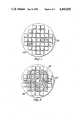
- FIG. 1shows a wafer-scale integrated circuit as it is physically laid out on a semiconducting substrate.
- FIG. 2shows the structure of the chain of individual cells on the wafer.
- FIG. 3shows the inter-cell coupling
- FIG. 4shows the internal structure of a cell.
- FIG. 5shows a simplified schematic drawing of the cells coupled in a chain.
- FIG. 1shows the physical layout of the wafer scale integrated circuit.
- a circular, semiconducting wafer substrate 10has fabricated thereon a plurality of square, shift register data storage cells 12.
- the cells 12form a regular tesselation across the surface of the wafer 10 with the exception of the omission of one cell from the the tesselation to form a coupling port 14.
- the coupling port 14is preferably but not necessarily at or near the the center of the wafer 10.
- the cells 12 bordering the coupling port 14are provided with coupling pads 16 by which they may be connected to the outside world.
- the cells 12are operable to couple to any selectable one neighbouring cell 12 for the transfer of data thereto and therefrom.
- one of the neighbouring cells 12 to the port 14is subjected to a functional test from the port 14 via the coupling pads 16. If the cell 12 is functional and therefore passes the functional test, it is instructed to couple to a further neighbouring cell 12 and that further cell 12 is tested.
- FIG. 2shows how the cells 12 can be formed into a data storage chain 18 on the wafer. It is to be understood that cells 12 which do not pass the functional test can be omitted from the chain 18 by its being steered around their positions.
- FIG. 3shows the connections on the boundaries of a cell 12.
- the square cell 12has four boundaries, designated the north boundary N, the south boundary S, the east boundary E and the west boundary W.
- the north boundary Nis contiguous with the south boundary S of a first neighbouring cell 12.
- the east boundary Eis contiguous with the west boundary W of a second neighbouring cell 12
- the south boundary Sis contiguous with the north boundary N of a third neighbouring cell 12
- the west boundary Wis contiguous with the east boundary E of a fourth neighbouring cell 12.
- Each boundary N, S, E, Whas a first line 20N, 20S, 20E, 20W respectively for transferring data out of the cell 12 to a neighbouring cell 12.
- Each boundary N, S, E, Whas a second line 22N, 22S, 22E, 22W respectively for transferring the master clock signal to a neighbouring cell 12.
- Each boundary N, S, E, Whas a third line 24N, 24S, 24E, 24W respectively for receiving the master clock signal from a neighbouring cell.
- Each boundary N, S, E, Whas a fourth line 26N, 26S, 26E, 26W for receiving data from a neighbouring cell.
- Table 1shows the interconnection between the lines shown and the lines on the neighbouring cells.
- a cell 12can pass data and clock signals to and receive data and clock signals from any neighbouring cell 12.
- FIG. 4shows the internal structure of a cell 12.
- the input and output lines to the cell 12are shown dissociated from their associated boundaries N, S, E, W to enhance the clarity of the figure.
- the data input lines 26N, 26S, 26E, 26Ware provided as the inputs to a forward data input gate 30 and to a reverse data input gate 32.
- the data output lines 20N, 20S, 20E, 20Ware provided as the output of a forward data output gate 34 and of a reverse data output gate 36.
- the forward data input gate 30selects the signal from one of the data input lines 26N, 26S, 26E, 26W for provision as input to a forward data shift register store 38.
- the reverse data input gate 32selects the signal from another of the data input lines 26N, 26S, 26E, 26W as the input to a reverse data shift register store 40.
- the forward data store 38 and the reverse data store 40can both be the same length and each comprise a plurality of shift register, bit storage cells coupled in tandem, or they can be of different lengths. After a predetermined number of clock pulses have been applied to a clock input to each of the stores 38, 40, the informational data originally presented at their input reappears at their output.
- the stores 38, 40according to various proposed and known cell configurations, can be means whereby data can be stored in or retrieved from other, main storage elements in the cell 12 as well as passed through the cell 12 up and down the chain 18.
- the output of the forward data store 38is provided as the input to the forward data output gate 34 which provides the output of the store 38 as the signal on a selectable one of the data output lines 20N, 20S, 20E, 20W.
- the output of the reverse data store 40is provided as the input to the reverse data output gate which provides the output of the reverse store 40 as the signal on another selectable one of the data output lines 20N, 20S, 20E, 20W.
- the master clock input lines 24N, 24S, 24E, 24Ware provided as the inputs to the master clock input gate which provides, as its output, the signal on a selectable one of the lines 24N, 24S, 24E, 24W.
- the output of the master clock input gateis provided firstly as the input to a master clock output gate 44 which provides, as its output, the signal on its input to a selectable one of the master clock output lines 22N, 22S, 22E, 22W.
- the output of the master clock input gate 42is provided secondly as the input to a clock signal generator 46.
- the clock signal generator 46generates a first clock signal on a first clock line 48 for controlling the data aquisition activity of the forward data input gate 30 and the data shifting activity of the forward store 38, and a second clock signal on a second clock line 50 for controlling the data aquisition activity of the reverse data input gate 32 and for controlling the data shifting activity of the reverse store 40.
- the switching action of the gates 30, 32, 34, 36, 42 and 44is determined by the state of a controller 52 which is coupled to control each of them to select in the case of the input gates 30, 32, 42, from which line a signal will be received or in the case of the output gates 34, 36, 44 to which line a signal will be delivered up.
- the exact manner in which the controller 52 receives instructions to be in a particular statedoes not constitute part of the present invention.
- the state of the controller 52can be established via Global control signals, command words intermingled with data, and the like, those skilled in the art being aware of numerous other ways in which this aim can be accomplished.
- the switching control action of the controller 52is shown in table 2. As is seen, at any one time one face N, S, E or W of the cell 12 is selected as the source of forward data, as a source of the master clock signal, and as a sink for the reverse data, and another face N, S, E or W of the cell 12 is chosen as the sink for the forward data, as the sink for the master clock signal, and as the source of the reverse data.
- FIG. 5shows a simplified configuration of the memory chain 18 which is formed on the wafer scale circuit.
- the forward registers 38 of the cells 12are coupled in series.
- the reverse registers 40 of the cells 12are similarly coupled in series.
- the chain of forward registers 38leads data from the port 14 to a last cell 12' and the chain of reverse registers 40' lead data back from the last cell 12' to the port 14.
- the last cell 12'has a loop data coupling 60 whereby the output of the last cell forward register 38' is provided as the input to the last cell reverse register 40'. All cells 12 have the facility for forming the loop coupling 60, but it is only used in that cell 12' which happens to find itself at the end of the chain.
- the master clock signalis coupled from the port 16 from clock generator 46 to clock generator 46 along the chain 18 up to and including the clock generator 46' of the last cell 12'. There being no cell 12 beyond the last cell 12', the propagation of the master clock signal stops thereat.
- the master clock signalis passed on by the clock generators 46 from cell 12 to cell, and is subject to a delay between the cells. If the delay in propagating the clock signal between cells 12 is designated by Td, then the clock signal will reach the Nth cell away from the port NTd later than if it had been propagated in the usual manner by parallel Global lines to all cells at the same time. If the last cell 12' is the Mth cell counting from the port 14, then forward data enters the last cell 12' MTd late. However, the same clock signal is used to clock the forward data as is used to control the flow of reverse data. The flow of data, in passing from the forward to the reverse direction, experiences an advance in position relative to the propagated clock signal which increases with the distance a cell 12 is away from the last cell 12' in the direction of the port 14.
- the clocked forward datain coming back from the last cell 12', encounters the forward propagated master clock signal not with increasing lateness, as had been the case in the propagation of the data in the forward chain, but with increasing earliness.
- This lateness and earlinessis of course measured with respect to the application of the master clock signal at the port 14 to the first cell 12.
- the present inventionworks equally well in any chain-connectable wafer-scale integrated circuit having a forward data path and a reverse data path. Those skilled in the art will be aware of many variations on this type of chain connectable wafer-scale circuit.
- the present inventionmight be employed in a wafer-scale circuit wherein data enters a directional chain at one port and leaves at another, the clock signal being propagated therebetween from the data entry port to the data exit port.
- the inventionequally applies to those circuits where data is propagated only so far down a chain for storage in a selectable cell, and where data is retrieved from storage from a selectable cell in the chain to be propagated back to a port.
- the clock generator 46can be of any kind consistent with the operation of the particular type of cell in conjunction with which the present invention is applied.
- the clock generator 46includes clock signal buffering means to prevent progressive attenuation of the master clock signal as it progresses down the chain.
- the cellsneed not be four-sided, nor need the clock and data signals be propagatable across every edge of the cells.
- the cellsneed not necessarily be all of the same shape or function.
- the present inventionmight equally be used to clock data into and out of, for example, arithmetic units in a wafer scale processor integrated circuit.
Landscapes
- Semiconductor Integrated Circuits (AREA)
Abstract
Description
TABLE 1 ______________________________________ INTER-CELL CONNECTIONS ______________________________________ 20N joins to 26S of neighbouring cell toNorth 22N joins to 24S of neighbouring cell toNorth 24N joins to 22S of neighbouring cell toNorth 26N joins to 20S of neighbouring cell toNorth 20E joins to 26W of neighbouring cell toEast 22E joins to 24W of neighbouring cell toEast 24E joins to 22W of neighbouring cell toEast 26E joins to 20W of neighbouring cell toEast 20S joins to 26N of neighbouring cell toSouth 22S joins to 24N of neighbouring cell toSouth 24S joins to 22N of neighbouring cell to South 26S joins to 20N of neighbouring cell toSouth 20W joins to 26E of neighbouring cell toWest 22W joins to 24E of neighbouring cell toWest 24W joins to 22E of neighbouring cell toWest 26W joins to 20E of neighbouring cell to West ______________________________________
TABLE 2 __________________________________________________________________________INPUT AND OUTPUT ROUTING FUNCTION OF THE CELL (12) SOURCE OF SOURCE OF SINK FOR SOURCE OF SINK FOR SINK FOR FORWARD DATA MASTER FORWARD REVERSE REVERSE MASTER CLOCK INPUT CLOCK INPUT DATA OUTPUT DATA INPUT DATA OUTPUT OUTPUT (TO 38) (TO 46,44) (FROM 38) (TO 40) (FROM 40) (FROM 42) __________________________________________________________________________26N 24NNOT 20N NOT 26N 20NNOT 22N26S 24S NOT20S NOT 22N26S 20S NOT 22S26E 24ENOT 20E NOT 26E 20E NOT 22E26W 24WNOT 20W NOT 26W 20WNOT 22WNOT 26N NOT 24N20N 26N NOT 20NNOT 26S NOT 24S20S 22W __________________________________________________________________________26S NOT 20S 22SNOT 26E NOT 24E20E 26E NOT 20E 22ENOT 26W NOT 24W20W 26W NOT 20W
Claims (22)
Applications Claiming Priority (2)
| Application Number | Priority Date | Filing Date | Title |
|---|---|---|---|
| GB8039902AGB2089536B (en) | 1980-12-12 | 1980-12-12 | Improvement in or relating to wafer scale integrated circuits |
| GB8039902 | 1980-12-12 |
Publications (1)
| Publication Number | Publication Date |
|---|---|
| US4493055Atrue US4493055A (en) | 1985-01-08 |
Family
ID=10517951
Family Applications (1)
| Application Number | Title | Priority Date | Filing Date |
|---|---|---|---|
| US06/330,539Expired - LifetimeUS4493055A (en) | 1980-12-12 | 1981-12-14 | Wafer-scale integrated circuits |
Country Status (2)
| Country | Link |
|---|---|
| US (1) | US4493055A (en) |
| GB (1) | GB2089536B (en) |
Cited By (12)
| Publication number | Priority date | Publication date | Assignee | Title |
|---|---|---|---|---|
| US4675717A (en)* | 1984-10-09 | 1987-06-23 | American Telephone And Telegraph Company, At&T Bell Laboratories | Water-scale-integrated assembly |
| US4773071A (en)* | 1986-10-02 | 1988-09-20 | Grumman Aerospace Corporation | Memory for storing response patterns in an automatic testing instrument |
| US4798976A (en)* | 1987-11-13 | 1989-01-17 | International Business Machines Corporation | Logic redundancy circuit scheme |
| US4868789A (en)* | 1985-12-13 | 1989-09-19 | Anamartic Limited | Random access memory system with circuitry for avoiding use of defective memory cells |
| US4943946A (en)* | 1985-07-12 | 1990-07-24 | Anamartic Limited | Control system for chained circuit modules |
| DE4033981A1 (en)* | 1989-10-26 | 1991-05-02 | Olympus Optical Co | Memory circuit board with semiconductor recording medium - has SRAM or EEPROM with preset wafer size for estimated storage capacity |
| US5072424A (en)* | 1985-07-12 | 1991-12-10 | Anamartic Limited | Wafer-scale integrated circuit memory |
| US5134539A (en)* | 1990-12-17 | 1992-07-28 | Nchip, Inc. | Multichip module having integral decoupling capacitor |
| US5203005A (en)* | 1989-05-02 | 1993-04-13 | Horst Robert W | Cell structure for linear array wafer scale integration architecture with capability to open boundary i/o bus without neighbor acknowledgement |
| US5214844A (en)* | 1990-12-17 | 1993-06-01 | Nchip, Inc. | Method of assembling integrated circuits to a silicon board |
| US5274270A (en)* | 1990-12-17 | 1993-12-28 | Nchip, Inc. | Multichip module having SiO2 insulating layer |
| US10964682B2 (en)* | 2016-09-30 | 2021-03-30 | Intel Corporation | Data storage system using wafer-level packaging |
Families Citing this family (1)
| Publication number | Priority date | Publication date | Assignee | Title |
|---|---|---|---|---|
| GB2236415B (en)* | 1989-09-28 | 1993-05-19 | Anamartic Ltd | Improvements relating to inter-chip timing for circuit modules |
Citations (5)
| Publication number | Priority date | Publication date | Assignee | Title |
|---|---|---|---|---|
| US3913072A (en)* | 1972-08-03 | 1975-10-14 | Ivor Catt | Digital integrated circuits |
| US3972031A (en)* | 1974-08-15 | 1976-07-27 | Zonic Technical Laboratories, Inc. | Variable length shift register alternately operable to store and recirculate data and addressing circuit therefor |
| GB2021825A (en)* | 1978-05-25 | 1979-12-05 | Aubusson R C | Improvements in or relating to semi conductor circuits |
| GB2035637A (en)* | 1978-11-08 | 1980-06-18 | Vmei Lenin Nis | Digital stack memory devices |
| US4229699A (en)* | 1978-05-22 | 1980-10-21 | Data General Corporation | Multiple clock selection system |
- 1980
- 1980-12-12GBGB8039902Apatent/GB2089536B/ennot_activeExpired
- 1981
- 1981-12-14USUS06/330,539patent/US4493055A/ennot_activeExpired - Lifetime
Patent Citations (5)
| Publication number | Priority date | Publication date | Assignee | Title |
|---|---|---|---|---|
| US3913072A (en)* | 1972-08-03 | 1975-10-14 | Ivor Catt | Digital integrated circuits |
| US3972031A (en)* | 1974-08-15 | 1976-07-27 | Zonic Technical Laboratories, Inc. | Variable length shift register alternately operable to store and recirculate data and addressing circuit therefor |
| US4229699A (en)* | 1978-05-22 | 1980-10-21 | Data General Corporation | Multiple clock selection system |
| GB2021825A (en)* | 1978-05-25 | 1979-12-05 | Aubusson R C | Improvements in or relating to semi conductor circuits |
| GB2035637A (en)* | 1978-11-08 | 1980-06-18 | Vmei Lenin Nis | Digital stack memory devices |
Cited By (13)
| Publication number | Priority date | Publication date | Assignee | Title |
|---|---|---|---|---|
| US4675717A (en)* | 1984-10-09 | 1987-06-23 | American Telephone And Telegraph Company, At&T Bell Laboratories | Water-scale-integrated assembly |
| US5072424A (en)* | 1985-07-12 | 1991-12-10 | Anamartic Limited | Wafer-scale integrated circuit memory |
| US4943946A (en)* | 1985-07-12 | 1990-07-24 | Anamartic Limited | Control system for chained circuit modules |
| US4868789A (en)* | 1985-12-13 | 1989-09-19 | Anamartic Limited | Random access memory system with circuitry for avoiding use of defective memory cells |
| US4773071A (en)* | 1986-10-02 | 1988-09-20 | Grumman Aerospace Corporation | Memory for storing response patterns in an automatic testing instrument |
| US4798976A (en)* | 1987-11-13 | 1989-01-17 | International Business Machines Corporation | Logic redundancy circuit scheme |
| US5203005A (en)* | 1989-05-02 | 1993-04-13 | Horst Robert W | Cell structure for linear array wafer scale integration architecture with capability to open boundary i/o bus without neighbor acknowledgement |
| US5287472A (en)* | 1989-05-02 | 1994-02-15 | Tandem Computers Incorporated | Memory system using linear array wafer scale integration architecture |
| DE4033981A1 (en)* | 1989-10-26 | 1991-05-02 | Olympus Optical Co | Memory circuit board with semiconductor recording medium - has SRAM or EEPROM with preset wafer size for estimated storage capacity |
| US5134539A (en)* | 1990-12-17 | 1992-07-28 | Nchip, Inc. | Multichip module having integral decoupling capacitor |
| US5214844A (en)* | 1990-12-17 | 1993-06-01 | Nchip, Inc. | Method of assembling integrated circuits to a silicon board |
| US5274270A (en)* | 1990-12-17 | 1993-12-28 | Nchip, Inc. | Multichip module having SiO2 insulating layer |
| US10964682B2 (en)* | 2016-09-30 | 2021-03-30 | Intel Corporation | Data storage system using wafer-level packaging |
Also Published As
| Publication number | Publication date |
|---|---|
| GB2089536B (en) | 1984-05-23 |
| GB2089536A (en) | 1982-06-23 |
Similar Documents
| Publication | Publication Date | Title |
|---|---|---|
| US4493055A (en) | Wafer-scale integrated circuits | |
| Koren | A reconfigurable and fault-tolerant VLSI multiprocessor array | |
| AU638454B2 (en) | Linear array wafer scale integration architecture | |
| US9455707B2 (en) | Superconductive gate system | |
| US4467422A (en) | Array processor | |
| US5086427A (en) | Clocked logic circuitry preventing double driving on shared data bus | |
| KR19990008270A (en) | Scalable multilevel interconnect architecture | |
| JPS59203299A (en) | Clock generator of memory with redundancy bit | |
| US20240005986A1 (en) | Superconducting distributed bidirectional current driver system | |
| US7733734B2 (en) | Semiconductor memory device with control block sharing row decoders | |
| US20090066164A1 (en) | Power Controlling Integrated Circuit Cell | |
| EP0097148B1 (en) | Improvements in or relating to wafer scale integrated circuits | |
| US4471483A (en) | Branched labyrinth wafer-scale integrated circuit | |
| US5287345A (en) | Data handling arrays | |
| US4633439A (en) | Superconducting read-only memories or programable logic arrays having the same | |
| Hashimoto et al. | Implementation of a 4/spl times/4 switch with passive interconnects | |
| KR100518597B1 (en) | Semiconductor memory device for consuming low power capable of changing input output data width selectively and data input/output method of the same | |
| EP0217905A1 (en) | Wafer scale integrated circuit | |
| CN101083142A (en) | Semiconductor device | |
| US4096580A (en) | Multiple redundancy loop bubble domain memory | |
| US6577159B1 (en) | Method and apparatus for automatic high-speed bypass routing in a cell matrix self-configurable hardware system | |
| JPH04254998A (en) | Redundancy circuit for semiconductor memory | |
| CA1201529A (en) | Superconducting read-only memories or programable logic arrays having the same | |
| EP0172311A2 (en) | Memory element for a wafer scale integrated circuit | |
| KR0157340B1 (en) | Array method for cell array of semiconductor memory device |
Legal Events
| Date | Code | Title | Description |
|---|---|---|---|
| AS | Assignment | Owner name:BURROUGHS CORPORATION, DETROIT, MI A CORP. OF MI Free format text:ASSIGNMENT OF ASSIGNORS INTEREST.;ASSIGNOR:OSMAN, ISMET M. F. M.;REEL/FRAME:003968/0766 Effective date:19811201 | |
| AS | Assignment | Owner name:BURROUGHS CORPORATION Free format text:MERGER;ASSIGNORS:BURROUGHS CORPORATION A CORP OF MI (MERGED INTO);BURROUGHS DELAWARE INCORPORATED A DE CORP. (CHANGED TO);REEL/FRAME:004312/0324 Effective date:19840530 | |
| STCF | Information on status: patent grant | Free format text:PATENTED CASE | |
| AS | Assignment | Owner name:ADVANCED TECHNOLOGY VENTURES, FOR ITSELF AND AS AG Free format text:SECURITY INTEREST;ASSIGNOR:MOSAIC SYSTEMS, INC., A DE CORP;REEL/FRAME:004583/0088 Effective date:19860430 | |
| AS | Assignment | Owner name:MOSAIC SYSTEMS, INC. Free format text:RELEASED BY SECURED PARTY;ASSIGNOR:ADVANCED TECHNOLOGY VENTURES;REEL/FRAME:004755/0730 Effective date:19870304 | |
| FPAY | Fee payment | Year of fee payment:4 | |
| AS | Assignment | Owner name:ADVANCED TECHNOLOGY VENTURES Free format text:SECURITY INTEREST;ASSIGNOR:MOSAIC SYSTEMS, INC.;REEL/FRAME:004993/0243 Effective date:19880826 | |
| AS | Assignment | Owner name:UNISYS CORPORATION, PENNSYLVANIA Free format text:MERGER;ASSIGNOR:BURROUGHS CORPORATION;REEL/FRAME:005012/0501 Effective date:19880509 | |
| AS | Assignment | Owner name:ROTHSCHILD VENTURES, INC. Free format text:SECURITY INTEREST;ASSIGNOR:MOSAIC SYSTEMS, INC.;REEL/FRAME:005244/0803 Effective date:19890228 | |
| AS | Assignment | Owner name:MOSAIC SYSTEMS, INC., CALIFORNIA Free format text:RELEASED BY SECURED PARTY;ASSIGNOR:ROTHSCHILD VENTURES, INC.;REEL/FRAME:005505/0647 Effective date:19900125 | |
| FEPP | Fee payment procedure | Free format text:PAYOR NUMBER ASSIGNED (ORIGINAL EVENT CODE: ASPN); ENTITY STATUS OF PATENT OWNER: LARGE ENTITY | |
| FPAY | Fee payment | Year of fee payment:8 | |
| FPAY | Fee payment | Year of fee payment:12 |