US4486846A - Numerically controlled oscillator using quadrant replication and function decomposition - Google Patents
Numerically controlled oscillator using quadrant replication and function decompositionDownload PDFInfo
- Publication number
- US4486846A US4486846AUS06/392,852US39285282AUS4486846AUS 4486846 AUS4486846 AUS 4486846AUS 39285282 AUS39285282 AUS 39285282AUS 4486846 AUS4486846 AUS 4486846A
- Authority
- US
- United States
- Prior art keywords
- coarse
- fine
- digital
- quadrant
- values
- Prior art date
- Legal status (The legal status is an assumption and is not a legal conclusion. Google has not performed a legal analysis and makes no representation as to the accuracy of the status listed.)
- Expired - Lifetime
Links
Images


Classifications
- G—PHYSICS
- G06—COMPUTING OR CALCULATING; COUNTING
- G06F—ELECTRIC DIGITAL DATA PROCESSING
- G06F1/00—Details not covered by groups G06F3/00 - G06F13/00 and G06F21/00
- G06F1/02—Digital function generators
- G06F1/03—Digital function generators working, at least partly, by table look-up
- G06F1/035—Reduction of table size
- G06F1/0356—Reduction of table size by using two or more smaller tables, e.g. addressed by parts of the argument
- G—PHYSICS
- G06—COMPUTING OR CALCULATING; COUNTING
- G06F—ELECTRIC DIGITAL DATA PROCESSING
- G06F2101/00—Indexing scheme relating to the type of digital function generated
- G06F2101/04—Trigonometric functions
Definitions
- Conventional frequency synthesizersaccomplish the generation of many different frequencies from one or more stable sources by means of analog circuits or by a combination of analog and digital circuits. In these approaches, the generation of frequencies is performed in the analog or continuous sense by division, phase lock, mixing, or some combination of these techniques.
- NCOnumerically controlled oscillator
- the present inventionpertains to a function generator and more particularly to a function generator for use in or as a numerically controlled oscillator.
- the present inventionis a function generator for generating generally sinusoidal waves having a digitally controlled frequency, said generator including coarse digital memory means for storing a plurality of digital values coarsely defining one quadrant of a sinusoidal wave, fine digital memory means for storing a plurality of digital values which when added to predetermined values stored in said coarse memory means substantially define the one quadrant of the sinusoidal wave, digital addition means connected to combine outputs of said coarse and fine memories to substantially define the one quadrant of the sinusoidal wave, digital logic means for shifting the combined output values to substantially define second, third and fourth quadrants of the sinusoidal wave, and address generating means for controlling the coarse and fine memory means and the digital logic means to generate a continuous sinusoidal wave at a frequency dictated by an input digital signal.
- the output data from the function generatorcan be applied to a conventional D/A converter and a low pass filter which results in a nearly perfect sine wave at the desired frequency.
- the entire digital frequency control and generation circuitryis available on one low power, radiation hardened semiconductor chip.
- the stability of the function generator/synthesizeris determined by the stability of one external fixed frequency oscillator. There are no analog control elements or variable oscillators to introduce instability.
- the outputis generated digitally from the single external oscillator, which can be built with higher radiation resistance, better thermal and aging characteristics, and greater stability than would be possible if analog control elements and variable oscillators were required.
- FIG. 1is a block diagram of the address generating portion of a numerically controlled oscillator embodying the present invention
- FIG. 2is a block diagram of the remaining portion of the numerically controlled oscillator illustrated in FIG. 1, illustrating the memories and combining portions of the generator;
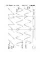
- FIGS. 3A, B, C and Dare analog representations of the output of the digital address generator of FIG. 1, the sinusoidally varying digital output of the combining circuits of FIG. 2, the 90° phase shifted sinusoidally varying digital output of the combining circuits of FIG. 2, and a waveform illustrating step phase shifts applied to the apparatus of FIG. 1, respectively;
- FIG. 4is a diagram of the inputs and outputs of a chip containing the numerically controlled oscillator of FIGS. 1 and 2;
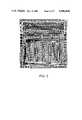
- FIG. 5is a view in top plan of a semiconductor chip including the apparatus illustrated in block form in FIGS. 1 and 2;
- FIG. 6is a simplified block diagram of a modification of the apparatus illustrated in FIG. 2.
- FIGS. 1 and 2A specific embodiment of the present invention is illustrated in FIGS. 1 and 2. The following is a general description of the construction and operation of the specific embodiment illustrated.
- a 16 line input data bus, designated 30,serves as an input for all phase and frequency information.
- the 16 bit busis designed to interface compatably with microprocessors and the like and is connected to an input latch 32 which is enabled by a system strobe signal.
- the input latch 32is enabled by the system strobe to facilitate proper input latching of potentially asynchronous input data on the data bus 30.
- a second set of latches 34, 35, and 36are operated by a system clock, which is a steady, crystal-controlled clock (not shown) that is the reference used to clock all internal timing of the numerically controlled oscillator.
- the second set of latches 34, 35, and 36are connected to the input latch 32 and the data contained in the latch 32 is transferred, on the occurrence of the next system clock pulse.
- the function of the two sets of latchesis to re-time the data before it is input to the succeeding circuitry.
- Latch 34is a phase latch for 10 bits of information representative of the desired phase of the output signal, as instructed by the input data.
- the phase latch 34supplies the 10 bits of phase data to an add circuit or accumulator 38 and to a first input of a multiplexer 40.
- the output of the accumulator 38is supplied to a second input of the multiplexer 40.
- the multiplexer 40selects the 10 bits supplied to the first input from the latch 34 and supplies it to a latch 42 which is operated by a phase strobe.
- the phase strobeis internal timing pulses necessary to properly coordinate the phase data which is to be input to the next stage.
- phase integrate modea signal is supplied to a control input of the multiplexer 40 to select the output from the accumulator 38.
- the output from the latch 42is supplied to a second input of the accumulator 38 to supply the required feedback for integration in the integrate mode of operation.
- the 10 bit word at the output of the latch 42represents a desired output phase.
- the latch 35is a latch for 8 bits of the input data representing high frequency while the latch 36 is a latch for 16 bits of the input data representing low frequency and the two are combined to form a 24 bit word which is supplied to a first input of an add circuit or accumulator 44 and to a first input of a multiplexer 46.
- the output of the accumulator 44is supplied to a second input of the multiplexer 46 and a control input of the multiplexer 46 controls the multiplexer between the first input in a normal mode of operation and the second input in a frequency low-order bits integrate mode (FLIM).
- FLIMfrequency low-order bits integrate mode
- the output of the multiplexer 46is supplied to a latch 48 which is controlled by a frequency strobe consisting of internal timing pulses necessary to properly coordinate the frequency data which is to be input to the next stages.
- the output of the latch 48is fed back to a second input of the accumulator 44 to provide the integration in the integrating mode of operation.
- the output of the latch 48is a 24 bit word representing a desired output frequency.
- the two most significant bits of the 10 bit phase word from the latch 42are supplied to an input of an add circuit 50.
- the add circuit 50has two other inputs for receiving phase shift commands of 180° and 90° (see FIG. 3D).
- the two most significant bitsare modified if a 180° or 90° command is supplied to the add circuit 50, otherwise they remain constant and are supplied along with the 8 least significant bits to a first input of a second add circuit 52.
- the 24 bit frequency word from the latch 48must be added to the 24 bit binary value stored in latches 70, 64, 58 on every system clock pulse to produce the linearly stepped digital signal illustrated in FIG. 3A.
- a parallel 24 bit adderwould slow down the system considerably so a concept known as pipelining is used here to increase the speed three-fold. Although throughput speed is increased by the pipelining concept, throughput delay is concommittently increased by 3 system clock periods.
- the 24 bit frequency wordis supplied to a clocked latch 54.
- the 8 least significant bits of the 24 bit input wordare supplied to a first input of an add circuit 56, the output of which is supplied to a clocked latch 58 and the output of the clocked latch is supplied to a second input of the add circuit 56.
- Carry signals from the addition processare supplied through the latch 58 to the carry input of an add circuit 60.
- the 16 remaining bits of the 24 bit wordare supplied from the latch 54 to a clocked latch 62.
- 8 of the 16 bits supplied to the latch 62are supplied to a first input of the add circuit 60, the output of which is supplied to a clocked latch 64.
- the 8 output bits of the latch 64are supplied to a second input of the add circuit 60 to provide the constant updating.
- the two most significant bits in the output of the latch 64are supplied through a clocked latch 65 as two least significant bits of a 10 bit frequency word.
- the remaining 8 bits from the latch 62are supplied to a clocked latch 66, the output of which is supplied to a first input of an add circuit 68.
- the output of the add circuit 68is connected to a clocked latch 70, the output of which is connected to a second input of the add circuit 68 to produce the constant updating of the frequency word.
- the 8 bits out of the latch 70are also combined with the two bits from the latch 65 to produce a 10 bit frequency word which is connected to a second input of the add circuit 52.
- the 10 bit phase word supplied to the first input of the add circuit 52is added to the 10 bit frequency word supplied to the second input of the add circuit 52 to produce a 10 bit address word which is supplied to a clocked latch 72.
- the 10 bit address word available at the output of the latch 72is depicted by the waveform illustrated in FIG. 3A. It should be noted that the word is continuously updated at each system clock pulse. Also, at a first point 74 a 90° phase shift command is inserted (FIG. 3D) into the add circuit 50 and at a second point 76 a 180° phase shift command is inserted (FIG. 3D) into the add circuit 50 to illustrate the operation of the circuits.
- phase increments of 90° and 180°are instantly available by simple commands, and any other phase increment from 0° to 360° in 0.35° steps is available by means of the input data at the data bus 30.
- Frequency steps of 0.24 Hzare available over the entire operating range of DC to 1 MHz through the information supplied at the data bus 30.
- the 24 bit frequency word at the output of the latch 48adjusts the constantly updated addresses developed by the pipelined accumulator to alter the number of steps in the address waveform of FIG. 3A and, thereby, alter the frequency at the output of the numerically controlled oscillator. It will of course be understood that the size and number of phase and frequency adjustments available depends upon the number of bits utilized in the various words throughout the system disclosed and more or less steps can be incorporated by utilizing more or less bits.
- the two most significant bits of the 10 bit address word from the latch 72are supplied to a clocked latch 80 as a quadrant control.
- a third input 81 to the latch 80serves as an output sine/cosine lag/lead control which allows the output quadrature sine and cosine signals to instantly be switched in phase with respect to each other.
- Six of the bits of the 10 bit wordare supplied, by way of a bus 82, to a fine sine read-only-memory (ROM) 84 and to a fine cosine ROM 86.
- Six of the bits of the 10 bit address word from the latch 72are supplied by way of a bus 88 to a coarse sine ROM 90 and to a coarse cosine ROM 92.
- the ROMs 84, 86, 90 and 92serve as lookup tables with the desired data being addressed by the 6 bit words supplied to the busses 82 and 88.
- the output data from the ROMs 84, 86, 90 and 92are supplied to clocked latches 94, 96, 100, and 102, respectively.
- the clocked latches 94 and 96then supply data to first inputs of add circuits 104 and 105, respectively, and the clocked latches 100 and 102 supply data to second inputs of the add circuits 104 and 105, respectively.
- the sum data, including the carry, from the add circuit 104is supplied through OR gates 107 to a first input of a multiplexer 109 and to a second input of a multiplexer 110.
- the OR gates 107are included to compensate for the single instance where all of the bits from the add circuit 104 are 1 and a 1 is added, which without compensation would provide an all 0 (or erroneous) output.
- the output data from the add circuit 105is supplied directly to a first input of the multiplexer 110 and a second input of the multiplexer 109.
- both size and speed barriersexist which tend to preclude the incorporation of a waveform generation ROM on the same semiconductor chip as the generator and remainder of the circuitry. Since the function performed by the ROM is essential to generation of high spectral purity waveforms, these barriers necessitate the high power consumption of off chip ROMs, with interconnection and associated propagation delays limiting the attainable operating speed of the functional ensemble.
- any attempt to apply the decomposition technique without carefully considering the effects of significant amplitude quantization effectswill yield unsatisfactory results; the resultant spectral purity will generally correspond to that obtainable using only the coarse phase bits.
- the difficulty associated with exploiting the decomposition propertyis compounded enormously because the NCO is so constrained for space and speed that it must make use of a second ROM size reduction technique, to be explained presently, referred to as the quadrant replication property. It is not obvious that the decomposition and quadrant replication properties are compatible in a quantized processor.
- the taskconsists of creating the best discrete-point fit to the error waveform subject to constraints on the number of bits available for both phase and amplitude resolution of the fine ROM values.
- the constraint upon the number of phase bitsis quite complicated, involving a subtle interaction of system design and chip architecture desirerata.
- the access time of the coarse and fine ROMsmust be identical (i.e., same number of address bits); otherwise, the slower one is limiting the maximum operating speed.
- reduction of address decoder sizedictates that the MSBs of the coarse and fine ROM addresses be identical.
- the phase address input to the waveform generatoris partitioned as shown below.
- the optimization routineoperates by choosing the best possible fit (correction) to the error waveform for any specified manner of partitioning the phase address word, generating in the process the rms and maximum residual error associated with that particular partition.
- the selection of the particular implementationreduces to matching the speed/size characteristics of the waveform generation portion of the speed/size characteristics of the rest of the chip.
- ROM addressesno greater than 6-bit ROM addresses were practical.
- a 10-bit ROM wordprovided the necessary speed match to this address size, and the 10-bit amplitude quantization dictated a 10-bit phase quantization.
- the attainable rms error associated with the selected architectureis only 2 units (1 bit) out of 13 bits, where 13 bits were carried for the ideal value to guarantee effectively "infinite resolution" relative to the 10-bit quantization effects under consideration.
- the maximum erroris seen to be only 0.75 of the LSB in a 10-bit representation. Effectively, this approach provides a full 10-bits of both phase and amplitude resolution.
- Table 3The effective savings in ROM size is summarized in Table 3.
- the 10-bit output words from the multiplexers 109 and 110are each supplied to 10 exclusive OR gates 112 and 114, respectively.
- Outputs of the latch 80are supplied directly to the select inputs of the multiplexers 109 and 110 and to a pair of exclusive OR gates 116 and 117, the outputs of which are connected to the exclusive OR gates 112 and 114, respectively.
- the quadrant replication propertyis implemented by means of the multiplexers 109 and 110, the latch 80, the exclusive OR gates 112, 114, 116 and 117.
- the sine and cosine values in each of the other three quadrantsmay be obtained by changing polarity and exchanging sine and cosine VALUES according to the scheme defined by Table 1 above.
- This schemereduces the required memory by a factor of 4, trading off the reduced memory for additional multiplexing and arithmatic operations. It is possible to further reduce the arithmatic complexity by converting the polarity inversion operation, requiring an M-bit ripple-add, to a simple parallel inversion of all M-bits; this conversion requires only that an appropriate bias be added to each sinusoidal value.
- the quadrant controls supplied to the latch 80select the correct input at each of the multiplexers 109 and 110 and the exclusive OR gates 112 and 114 provide inversion when required according to Table 1.
- a continuous digital sinusoidal waveis provided at the output of each of the exclusive OR gates 112 and 114, which sinusoidal waves are supplied to clock latches 118 and 119, respectively.
- the sinusoidal wave applied to the latch 118is illustrated in FIG. 3B and the sinusoidal wave applied to the latch 119 is illustrated in FIG. 3C.
- continuous sinusoidal wavesit is meant that the four quadrants are assembled in a continuous fashion (as illustrated in FIG. 3) and so that no discontinuities appear at the demarkation points of each quadrant.
- Digital-to-analog converters 120 and 121are connected to receive the outputs of the latches 118 and 119, respectively, the digital-to-analog converters 120 and 121 are external to the chip containing the NCO. Additional smoothing filters may be incorporated if desired to obtain the analog version of the output frequency.
- the numerically controlled oscillator disclosed in FIGS. 1 and 2is illustrated as a semiconductor chip 125 with the inputs and outputs thereto illustrated.
- the 16 line data bus 30is used to input all phase and frequency information.
- a three line function select bus 127selects one of 8 possible modes of operation and can be modified every 4 system clock periods. The various modes of operation are illustrated in Table 4 below.
- a single input line 128is connected to the external system clock, which is a steady, crystal controlled clock that is the reference used to clock all internal timing of the numerically controlled oscillator.
- a single input line 129is a system strobe input to the numerically controlled oscillator internal system timing to facilitate proper input latching of potentially asynchronous input data (on the 16 line data bus 30).
- a single input line 130receives a reset signal which allows the numerically controlled oscillator programmer to set all accumulators and registers internal to the NCO to a 0 state.
- a single input line 132receives an output sine/cosine lag/lead control signal which allows the output quadrature sine and cosine signals to instantly be switched in phase 180 with respect to each other.
- a test address input line 134, a test enable line 135 and a test address output line 136allow quick entry of test addresses to the numerically controlled oscillator's internal ROMs and allows rapid visibility of all bits of the 24 bit accumulator preceding the ROMS.
- An input line 138is adapted to receive a tri-state control signal which switches outputs to high impedence state of high/low logic levels.
- the chip 125includes a 6 lead output bus 140 which is attached to test transistors on the chip 125.
- the test transistorsare N and P channel thin oxide and an N channel thick oxide device to allow on chip monitoring of radiation degradation. Referring specifically to FIG. 5, a view in top plan of the actual chip 125 is illustrated, increased approximately 25 times in size. All of the apparatus illustrated in FIGS. 1 and 2 is contained on the chip 125, except the D to A converters 120 and 121.
- FIG. 6a simplified block diagram of a modification of the apparatus illustrated in FIG. 2 is illustrated. Components which are similar to those illustrated in FIG. 2 have a similar number designation with a prime added to indicate that it is a modified embodiment thereof.
- the 10 lead output bus from latch 72(FIG. 1) is connected to a 10 lead input 150.
- the two most significant bitsare connected to latch 80', as in the embodiment of FIG. 2 and the remaining 8 bits are supplied to 7 exclusive OR gates 152 and 7 exclusive OR gates 153.
- the most significant bit of the 8 bitsis connected to latch 80' and to a first input of each of the 7 exclusive OR gates 152 and, through an inverter 154, to a first input of each of the 7 exclusive OR gates 153.
- the 7 remaining bitsare each connected to a second input of a different one of the 7 exclusive OR gates 152 and to a second input of a different one of the 7 exclusive OR gates 153.
- Five of the seven leads from the exclusive OR gates 152are connected as an address to a first coarse ROM 156, 5 of the leads are connected as an address to a first fine ROM 158.
- 5 of the 7 output leads from the exclusive OR gates 153are connected as an address to a second coarse ROM 160 and 5 leads are connected to a second fine ROM 162.
- a second coarse ROM 160As in the embodiment illustrated in FIG.
- the outputs of the first coarse and fine ROMs 156 and 158are supplied to closed latches 94', 96', respectively, which then supply data to an add circuit 104' and the outputs of the ROMs 160 and 162 are supplied to clocked latches 100' and 102', respectively, which the supply data to an add circuit 105'.
- the outputs of the add circuits 104' and 105'are then connected to two inputs of a pair of multiplexers 109' and 110' as disclosed in the embodiment of FIG. 2.
- the multiplex selection circuit for the present embodimentdiffers from that of FIG. 2 in that an exclusive OR gate 170 is connected between the latch 80' and the selecting inputs of the multiplexers 109' and 110' for purposes that will become apparent presently.
- all of the values for defining a coarse approximation of the first quadrant of a sine or cosine waveare stored in the first or second coarse ROMs 156 and 160. All of the fine values to be added to the coarse values to specifically define the first quadrant are stored in the fine ROMs 158 and 162.
- the addressessimply step through the values stored in the first coarse ROM 156 and then continue to step through the values stored in the second coarse ROM 160. For purposes of this explanation this can be considered a forward sequence.
- the address supplied to the first coarse ROM 156 by the exclusive OR gates 152is stepping through the values stored therein in a forward sequence
- the address supplied to the second coarse ROM 160 by the exclusive OR gates 153can be stepping through the values therein in a reverse direction. Assuming that the same number of values are stored in both the first and second coarse ROMs 156 and 160, when the values in the first coarse ROM have been read out in a forward direction the values in the second coarse ROM will have been read out in a reverse direction and the order in which the values in each of the ROMs are supplied to the add circuits 104' and 105' can be reversed and multiplexer 109' selected to exchange the add circuits' outputs to complete the generation of a full quadrant.
- the second and fourth quadrantsare generated by reading the ROMs in reverse order for the sine and forward order for the cosine.
- fine ROMs 158 and 162can be addressed to supply the fine components required to complete a simulation of the desired quadrants.
- a single quadrant of a sine or cosine waveformis stored in the four ROMs of the embodiment illustrated in FIG. 6, whereas a first quadrant of a sine and cosine waveform are stored in the four ROMs of the embodiment of FIG. 2. It is estimated that this modification of the numerically controlled oscillator reduces the number of memory bits required in the ROMs by 832 bits.
- phase word applied to the ROMsis stepped linearly through a complete sequence, the phase word can actually be used as a coarse approximation of the sine wave.
- the values in the coarse ROMcan then be used to correct the coarse approximation rather than supply the whole value as in the embodiments illustrated. In this fashion fewer coarse ROM bits need to be stored. For example, the two most significant bits can be eliminated to reduce the storage required in the ROMs by another 128 bits.
- the values stored in the fine ROMsare periodically 0.
- the address to this ROMmay be partially decoded so that only one physical location containing 0 will respond to all addresses that should contain 0. Additional applications of this principle eliminating identical storage locations may be possible in specific cases.
- the elimination of the multiple stored O'ssaves 21 more bits in the storage and it is estimated that as many as 60 bits could be saved, or eliminated.
- a numerically controlled oscillatorwherein the entire digital frequency control and generation circuitry is available on one low power, radiation-hardened chip.
- the stability of the synthesizer/oscillatoris determined by the stability of one external fixed frequency oscillator.
- Frequency multiplying with the NCOcan be performed by connecting the 10 outputs of each chip to a multiplexer having a 10 lead input for each chip used and a single 20 lead output. The 10 bit output of the multiplexer is then supplied to a 10 bit D to A converter which must be capable of processing the incoming digital data fast enough to produce a clear sinusoidal wave at the output.
Landscapes
- Engineering & Computer Science (AREA)
- Theoretical Computer Science (AREA)
- Physics & Mathematics (AREA)
- General Engineering & Computer Science (AREA)
- General Physics & Mathematics (AREA)
- Stabilization Of Oscillater, Synchronisation, Frequency Synthesizers (AREA)
Abstract
Description
TABLE 1 __________________________________________________________________________SINUSOID QUADRANT REPLICATION FIRST QUADRANT SECOND THIRD FOURTH (Assumed QUADRANT QUADRANT QUADRANT known) (TBD) (TBD) (TBD) __________________________________________________________________________ SIN(X) SIN(X) = A ##STR1## SIN(X + π) = -A ##STR2## COS(X) COS(X) = B ##STR3## COS(X + π) = -B ##STR4## __________________________________________________________________________
______________________________________ NQ NA NC NF ______________________________________
TABLE 2 __________________________________________________________________________SUMMARY OF ROM COMPRESSION PERFORMANCE FOR AVAILABLE OPTIONS Number Of Amp. ERROR NA + NC = NA + NF NQ + NA + NC + NF = N NA Bits RMS(X2.sup.13) MAX(X2.sup.13) __________________________________________________________________________5 11 1 8 19.8 72 5 11 1 10 17.7 67 6 11 3 8 9.5 24 6 11 3 10 3.1 11 7 11 5 8 28.4 78 7 11 5 10 15.2 45 5 10 2 8 13.2 43 5 10 2 10 8.7 30 6 10 4 8 8.5 24 6 10 4 10 2.3 6 7 10 6 8 27.3 65 7 10 6 10 12.7 34 4 9 1 8 34.3 119 4 9 1 10 33.3 117 5 9 3 8 9.4 24 5 9 3 10 4.2 14 6 9 5 8 29.7 94 6 9 5 10 19.1 57 __________________________________________________________________________
TABLE 3 __________________________________________________________________________RELATIVE ROM SIZES FOR VARIOUS COMPRESSION TECHNIQUES ROM SIZE TO ACCOMMODATE 10-BIT PHASE AND TECHNIQUE AMPLITUDE RESOLUTION __________________________________________________________________________NO COMPRESSION 20,480 QUADRANT REPLICATION ONLY 5,120 QUADRANT REPLICATION PLUS 1,728 DECOMPOSITION __________________________________________________________________________
TABLE 4 __________________________________________________________________________MNCO FUNCTION SELECT COMMANDS MNEMONIC FUNCTION L .sup.--R I.sub.2 I.sub.1 I.sub.0 __________________________________________________________________________NOP NOOPERATION X 1 0 0 0 FLAM FREQUENCY LOW-ORDERBITS ADDITIVE X 1 0 0 1 P180 180°PHASE BUMP X 1 0 1 0 PIM PHASE INTEGRATEMODE X 1 0 1 1 P090 90°PHASE BUMP X 1 1 0 0 FHAM FREQUENCY HIGH-ORDER BITS X 1 1 0 1 ADDITIVE MODE PAM PHASEADDITIVE MODE X 1 1 1 0 FLIM FREQUENCY LOW-ORDER BITS X 1 1 1 1 INTEGRATE MODE RST RESET X 0 X X X LGLD LEAD (I = Q + 90°) 0 1 X X X LAG (I = Q - 90°) 1 1 X X X __________________________________________________________________________
Claims (17)
sin (X+Y)=sin X+Y cos X
cos (X+Y)=cos X-Y sin X
Priority Applications (1)
| Application Number | Priority Date | Filing Date | Title |
|---|---|---|---|
| US06/392,852US4486846A (en) | 1982-06-28 | 1982-06-28 | Numerically controlled oscillator using quadrant replication and function decomposition |
Applications Claiming Priority (1)
| Application Number | Priority Date | Filing Date | Title |
|---|---|---|---|
| US06/392,852US4486846A (en) | 1982-06-28 | 1982-06-28 | Numerically controlled oscillator using quadrant replication and function decomposition |
Publications (1)
| Publication Number | Publication Date |
|---|---|
| US4486846Atrue US4486846A (en) | 1984-12-04 |
Family
ID=23552277
Family Applications (1)
| Application Number | Title | Priority Date | Filing Date |
|---|---|---|---|
| US06/392,852Expired - LifetimeUS4486846A (en) | 1982-06-28 | 1982-06-28 | Numerically controlled oscillator using quadrant replication and function decomposition |
Country Status (1)
| Country | Link |
|---|---|
| US (1) | US4486846A (en) |
Cited By (42)
| Publication number | Priority date | Publication date | Assignee | Title |
|---|---|---|---|---|
| US4604719A (en)* | 1983-10-21 | 1986-08-05 | Crown International, Inc. | Oscillator having a sixteen bit signal generation utilizing an eight bit processor |
| US4618966A (en)* | 1983-06-01 | 1986-10-21 | Cincinnati Electronics Corporation | Frequency shift key modulator |
| US4631694A (en)* | 1984-04-27 | 1986-12-23 | National Semiconductor Corporation | Sine wave synthesizer |
| US4635279A (en)* | 1985-07-25 | 1987-01-06 | Rca Corporation | Arrangement for coherently generating sinusoids of different frequencies, and angle modulation data receiver using the arrangement |
| US4694417A (en)* | 1982-07-21 | 1987-09-15 | Raytheon Company | Method and apparatus for determining the magnitude of a square root of a sum of squared value using vernier addressing |
| US4715046A (en)* | 1986-06-20 | 1987-12-22 | Science Applications International Corporation | Frequency agile signal generator for emulating communications environments |
| US4740995A (en)* | 1983-08-24 | 1988-04-26 | Texas Instruments Incorporated | Variable frequency sinusoidal signal generator, in particular for a modem |
| WO1988004861A1 (en)* | 1986-12-23 | 1988-06-30 | Joseph Charles Lyons | Audible or visual digital waveform generating system |
| US4809205A (en)* | 1986-11-19 | 1989-02-28 | Rockwell International Corporation | Digital sine conversion circuit for use in direct digital synthesizers |
| US4819196A (en)* | 1985-10-17 | 1989-04-04 | Ampex Corporation | Digital-based phase control system |
| US4845436A (en)* | 1985-05-29 | 1989-07-04 | Trio Kabushiki Kaisha | Frequency synthesizer suited for use in a time division multiplexing system |
| US4855946A (en)* | 1987-10-22 | 1989-08-08 | Motorola, Inc. | Reduced size phase-to-amplitude converter in a numerically controlled oscillator |
| US4905177A (en)* | 1988-01-19 | 1990-02-27 | Qualcomm, Inc. | High resolution phase to sine amplitude conversion |
| US4926130A (en)* | 1988-01-19 | 1990-05-15 | Qualcomm, Inc. | Synchronous up-conversion direct digital synthesizer |
| US4958310A (en)* | 1987-11-19 | 1990-09-18 | Goldberg Bar Giora | Digital frequency synthesizer having multiple processing paths |
| US5010585A (en)* | 1990-06-01 | 1991-04-23 | Garcia Rafael A | Digital data and analog radio frequency transmitter |
| US5073869A (en)* | 1989-08-25 | 1991-12-17 | Titan Linkabit Corporation | Suppression of spurious frequency components in direct digital frequency synthesizer |
| WO1992002872A1 (en)* | 1990-08-02 | 1992-02-20 | Harris Corporation | Sin/cos generator implementation |
| EP0462714A3 (en)* | 1990-06-21 | 1992-02-26 | Tektronix, Inc. | Generation of phase related waveforms |
| US5329260A (en)* | 1992-07-17 | 1994-07-12 | Ii Morrow Inc. | Numerically-controlled modulated oscillator and modulation method |
| US5517535A (en)* | 1994-10-13 | 1996-05-14 | Westinghouse Electric Corp. | Numerically controlled oscillator with complex exponential outputs using recursion technique |
| US5631586A (en)* | 1995-01-06 | 1997-05-20 | Yamaha Corporation | Sine-wave generator circuit |
| US5673212A (en)* | 1995-09-01 | 1997-09-30 | Motorola, Inc. | Method and apparatus for numerically controlled oscillator with partitioned phase accumulator |
| WO1999012089A1 (en)* | 1997-09-02 | 1999-03-11 | Rohde & Schwarz Gmbh & Co. Kg | Digital sine wave generator |
| US5931891A (en)* | 1997-09-18 | 1999-08-03 | Landry; Michael William | Digital frequency synthesizer |
| US5952890A (en)* | 1997-02-05 | 1999-09-14 | Fox Enterprises, Inc. | Crystal oscillator programmable with frequency-defining parameters |
| US5960405A (en)* | 1997-02-05 | 1999-09-28 | Fox Enterprises, Inc. | Worldwide marketing logistics network including strategically located centers for frequency programming crystal oscillators to customer specification |
| USRE36388E (en)* | 1992-08-14 | 1999-11-09 | Harris Corporation | Sine/cosine generator and method |
| US6173301B1 (en)* | 1996-12-18 | 2001-01-09 | Nokia Telecommunications Oy | Method of generating signal amplitude responsive to desired function, and converter |
| WO2001007992A1 (en)* | 1999-07-27 | 2001-02-01 | Raytheon Company | Method and system for generating a trigonometric function |
| US6320431B1 (en) | 1999-10-08 | 2001-11-20 | National Semiconductor Corporation | Apparatus and method of generating numerically controlled oscillator signals |
| EP1213889A1 (en)* | 2000-12-07 | 2002-06-12 | Motorola, Inc. | Waveform generator for use in quadrature modulation (I/Q) |
| US6434582B1 (en)* | 1999-06-18 | 2002-08-13 | Advanced Micro Devices, Inc. | Cosine algorithm for relatively small angles |
| DE10129628A1 (en)* | 2001-06-20 | 2003-01-02 | Juergen Kaesser | Generating sinusoidal signals and clock signals for frequencies of pattern in radio equipment involves multiplying two pairs of digital values together and adding results of multiplication |
| US6587516B2 (en)* | 1989-08-14 | 2003-07-01 | Interdigital Technology Corporation | Subscriber unit producing a modulated digital frequency |
| US6590948B1 (en) | 2000-03-17 | 2003-07-08 | Raytheon Company | Parallel asynchronous sample rate reducer |
| US6647075B1 (en) | 2000-03-17 | 2003-11-11 | Raytheon Company | Digital tuner with optimized clock frequency and integrated parallel CIC filter and local oscillator |
| US6661852B1 (en) | 1999-07-21 | 2003-12-09 | Raytheon Company | Apparatus and method for quadrature tuner error correction |
| US20080084721A1 (en)* | 2006-09-13 | 2008-04-10 | Hypertherm, Inc. | Linear, inductance based control of regulated electrical properties in a switch mode power supply of a thermal processing system |
| US20090300088A1 (en)* | 2008-05-29 | 2009-12-03 | Harris Corporation | Sine/cosine generator |
| US9904311B1 (en) | 2016-08-09 | 2018-02-27 | Stmicroelectronics S.R.L. | System and a method for a waveform generator |
| US11226792B2 (en)* | 2019-07-01 | 2022-01-18 | Lapis Semiconductor Co., Ltd. | Trigonometric function calculating device |
Citations (9)
| Publication number | Priority date | Publication date | Assignee | Title |
|---|---|---|---|---|
| US3898446A (en)* | 1974-09-06 | 1975-08-05 | Us Army | Quadratic phase memory |
| US4068178A (en)* | 1976-10-01 | 1978-01-10 | Telenetics, Inc. | Variable frequency waveform synthesizer |
| US4134072A (en)* | 1977-09-06 | 1979-01-09 | Rca Corporation | Direct digital frequency synthesizer |
| US4159526A (en)* | 1977-08-08 | 1979-06-26 | Ncr Corporation | Digitally controlled variable frequency oscillator |
| US4159527A (en)* | 1978-01-19 | 1979-06-26 | Tokyo Shibaura Electric Co., Ltd. | Wave generator |
| US4172286A (en)* | 1977-01-18 | 1979-10-23 | Siemens Aktiengesellschaft | System for the generation of sine oscillations |
| US4342245A (en)* | 1979-10-26 | 1982-08-03 | Norlin Industries, Inc. | Complex waveform generator for musical instrument |
| US4346448A (en)* | 1978-11-23 | 1982-08-24 | The General Electric Company, Limited | Generation of electric signals having approximately sinusoidal waveforms |
| US4410955A (en)* | 1981-03-30 | 1983-10-18 | Motorola, Inc. | Method and apparatus for digital shaping of a digital data stream |
- 1982
- 1982-06-28USUS06/392,852patent/US4486846A/ennot_activeExpired - Lifetime
Patent Citations (9)
| Publication number | Priority date | Publication date | Assignee | Title |
|---|---|---|---|---|
| US3898446A (en)* | 1974-09-06 | 1975-08-05 | Us Army | Quadratic phase memory |
| US4068178A (en)* | 1976-10-01 | 1978-01-10 | Telenetics, Inc. | Variable frequency waveform synthesizer |
| US4172286A (en)* | 1977-01-18 | 1979-10-23 | Siemens Aktiengesellschaft | System for the generation of sine oscillations |
| US4159526A (en)* | 1977-08-08 | 1979-06-26 | Ncr Corporation | Digitally controlled variable frequency oscillator |
| US4134072A (en)* | 1977-09-06 | 1979-01-09 | Rca Corporation | Direct digital frequency synthesizer |
| US4159527A (en)* | 1978-01-19 | 1979-06-26 | Tokyo Shibaura Electric Co., Ltd. | Wave generator |
| US4346448A (en)* | 1978-11-23 | 1982-08-24 | The General Electric Company, Limited | Generation of electric signals having approximately sinusoidal waveforms |
| US4342245A (en)* | 1979-10-26 | 1982-08-03 | Norlin Industries, Inc. | Complex waveform generator for musical instrument |
| US4410955A (en)* | 1981-03-30 | 1983-10-18 | Motorola, Inc. | Method and apparatus for digital shaping of a digital data stream |
Cited By (56)
| Publication number | Priority date | Publication date | Assignee | Title |
|---|---|---|---|---|
| US4694417A (en)* | 1982-07-21 | 1987-09-15 | Raytheon Company | Method and apparatus for determining the magnitude of a square root of a sum of squared value using vernier addressing |
| US4618966A (en)* | 1983-06-01 | 1986-10-21 | Cincinnati Electronics Corporation | Frequency shift key modulator |
| US4740995A (en)* | 1983-08-24 | 1988-04-26 | Texas Instruments Incorporated | Variable frequency sinusoidal signal generator, in particular for a modem |
| US4604719A (en)* | 1983-10-21 | 1986-08-05 | Crown International, Inc. | Oscillator having a sixteen bit signal generation utilizing an eight bit processor |
| US4631694A (en)* | 1984-04-27 | 1986-12-23 | National Semiconductor Corporation | Sine wave synthesizer |
| US4845436A (en)* | 1985-05-29 | 1989-07-04 | Trio Kabushiki Kaisha | Frequency synthesizer suited for use in a time division multiplexing system |
| US4635279A (en)* | 1985-07-25 | 1987-01-06 | Rca Corporation | Arrangement for coherently generating sinusoids of different frequencies, and angle modulation data receiver using the arrangement |
| US4819196A (en)* | 1985-10-17 | 1989-04-04 | Ampex Corporation | Digital-based phase control system |
| US4715046A (en)* | 1986-06-20 | 1987-12-22 | Science Applications International Corporation | Frequency agile signal generator for emulating communications environments |
| US4809205A (en)* | 1986-11-19 | 1989-02-28 | Rockwell International Corporation | Digital sine conversion circuit for use in direct digital synthesizers |
| WO1988004861A1 (en)* | 1986-12-23 | 1988-06-30 | Joseph Charles Lyons | Audible or visual digital waveform generating system |
| US4855946A (en)* | 1987-10-22 | 1989-08-08 | Motorola, Inc. | Reduced size phase-to-amplitude converter in a numerically controlled oscillator |
| US4958310A (en)* | 1987-11-19 | 1990-09-18 | Goldberg Bar Giora | Digital frequency synthesizer having multiple processing paths |
| US4905177A (en)* | 1988-01-19 | 1990-02-27 | Qualcomm, Inc. | High resolution phase to sine amplitude conversion |
| US4926130A (en)* | 1988-01-19 | 1990-05-15 | Qualcomm, Inc. | Synchronous up-conversion direct digital synthesizer |
| US6724851B2 (en) | 1989-08-14 | 2004-04-20 | David Norton Critchlow | FIR chip for use in a wireless subscriber unit |
| US6587516B2 (en)* | 1989-08-14 | 2003-07-01 | Interdigital Technology Corporation | Subscriber unit producing a modulated digital frequency |
| US5073869A (en)* | 1989-08-25 | 1991-12-17 | Titan Linkabit Corporation | Suppression of spurious frequency components in direct digital frequency synthesizer |
| US5010585A (en)* | 1990-06-01 | 1991-04-23 | Garcia Rafael A | Digital data and analog radio frequency transmitter |
| EP0462714A3 (en)* | 1990-06-21 | 1992-02-26 | Tektronix, Inc. | Generation of phase related waveforms |
| WO1992002872A1 (en)* | 1990-08-02 | 1992-02-20 | Harris Corporation | Sin/cos generator implementation |
| US5113361A (en)* | 1990-08-02 | 1992-05-12 | Harris Corporation | Sin/cos generator implementation |
| US5329260A (en)* | 1992-07-17 | 1994-07-12 | Ii Morrow Inc. | Numerically-controlled modulated oscillator and modulation method |
| USRE36388E (en)* | 1992-08-14 | 1999-11-09 | Harris Corporation | Sine/cosine generator and method |
| US5517535A (en)* | 1994-10-13 | 1996-05-14 | Westinghouse Electric Corp. | Numerically controlled oscillator with complex exponential outputs using recursion technique |
| US5631586A (en)* | 1995-01-06 | 1997-05-20 | Yamaha Corporation | Sine-wave generator circuit |
| US5673212A (en)* | 1995-09-01 | 1997-09-30 | Motorola, Inc. | Method and apparatus for numerically controlled oscillator with partitioned phase accumulator |
| US6173301B1 (en)* | 1996-12-18 | 2001-01-09 | Nokia Telecommunications Oy | Method of generating signal amplitude responsive to desired function, and converter |
| US6954113B2 (en) | 1997-02-05 | 2005-10-11 | Fox Electronics, Inc. | Programmable oscillator circuit |
| US5952890A (en)* | 1997-02-05 | 1999-09-14 | Fox Enterprises, Inc. | Crystal oscillator programmable with frequency-defining parameters |
| US6664860B2 (en) | 1997-02-05 | 2003-12-16 | Fox Enterprises, Inc. | Programmable oscillator circuit and method |
| US6188290B1 (en) | 1997-02-05 | 2001-02-13 | Fox Enterprises, Inc. | Method of initializing an oscillator circuit |
| US6965272B2 (en) | 1997-02-05 | 2005-11-15 | Fox Enterprises, Inc. | Worldwide marketing logistics network including strategically located centers for frequency programming crystal oscillators to customer specification |
| US5960405A (en)* | 1997-02-05 | 1999-09-28 | Fox Enterprises, Inc. | Worldwide marketing logistics network including strategically located centers for frequency programming crystal oscillators to customer specification |
| WO1999012089A1 (en)* | 1997-09-02 | 1999-03-11 | Rohde & Schwarz Gmbh & Co. Kg | Digital sine wave generator |
| DE19738357B4 (en)* | 1997-09-02 | 2005-01-05 | Rohde & Schwarz Gmbh & Co. Kg | Method for operating a digital sine-wave generator |
| US5931891A (en)* | 1997-09-18 | 1999-08-03 | Landry; Michael William | Digital frequency synthesizer |
| US6434582B1 (en)* | 1999-06-18 | 2002-08-13 | Advanced Micro Devices, Inc. | Cosine algorithm for relatively small angles |
| US6661852B1 (en) | 1999-07-21 | 2003-12-09 | Raytheon Company | Apparatus and method for quadrature tuner error correction |
| US6640237B1 (en) | 1999-07-27 | 2003-10-28 | Raytheon Company | Method and system for generating a trigonometric function |
| WO2001007992A1 (en)* | 1999-07-27 | 2001-02-01 | Raytheon Company | Method and system for generating a trigonometric function |
| US6320431B1 (en) | 1999-10-08 | 2001-11-20 | National Semiconductor Corporation | Apparatus and method of generating numerically controlled oscillator signals |
| US6647075B1 (en) | 2000-03-17 | 2003-11-11 | Raytheon Company | Digital tuner with optimized clock frequency and integrated parallel CIC filter and local oscillator |
| US6590948B1 (en) | 2000-03-17 | 2003-07-08 | Raytheon Company | Parallel asynchronous sample rate reducer |
| WO2002047344A3 (en)* | 2000-12-07 | 2002-10-10 | Motorola Inc | Waveform generator for use in iq modulation |
| US20040019620A1 (en)* | 2000-12-07 | 2004-01-29 | Nadim Khlat | Waveform generator for use in iq modulation |
| EP1376968A1 (en)* | 2000-12-07 | 2004-01-02 | Motorola, Inc. | A transceiver |
| EP1213889A1 (en)* | 2000-12-07 | 2002-06-12 | Motorola, Inc. | Waveform generator for use in quadrature modulation (I/Q) |
| US7117234B2 (en) | 2000-12-07 | 2006-10-03 | Freescale Semiconductor, Inc. | Waveform generator for use in IQ modulation |
| DE10129628A1 (en)* | 2001-06-20 | 2003-01-02 | Juergen Kaesser | Generating sinusoidal signals and clock signals for frequencies of pattern in radio equipment involves multiplying two pairs of digital values together and adding results of multiplication |
| US20080084721A1 (en)* | 2006-09-13 | 2008-04-10 | Hypertherm, Inc. | Linear, inductance based control of regulated electrical properties in a switch mode power supply of a thermal processing system |
| US7911816B2 (en) | 2006-09-13 | 2011-03-22 | Hypertherm, Inc. | Linear, inductance based control of regulated electrical properties in a switch mode power supply of a thermal processing system |
| US20090300088A1 (en)* | 2008-05-29 | 2009-12-03 | Harris Corporation | Sine/cosine generator |
| US8200728B2 (en)* | 2008-05-29 | 2012-06-12 | Harris Corporation | Sine/cosine generator |
| US9904311B1 (en) | 2016-08-09 | 2018-02-27 | Stmicroelectronics S.R.L. | System and a method for a waveform generator |
| US11226792B2 (en)* | 2019-07-01 | 2022-01-18 | Lapis Semiconductor Co., Ltd. | Trigonometric function calculating device |
Similar Documents
| Publication | Publication Date | Title |
|---|---|---|
| US4486846A (en) | Numerically controlled oscillator using quadrant replication and function decomposition | |
| US4809205A (en) | Digital sine conversion circuit for use in direct digital synthesizers | |
| US4905177A (en) | High resolution phase to sine amplitude conversion | |
| US4482974A (en) | Apparatus and method of phase-to-amplitude conversion in a sine function generator | |
| US5371765A (en) | Binary phase accumulator for decimal frequency synthesis | |
| US4951237A (en) | Direct digital synthesizer with selectably randomized accumulator | |
| Vankka | Methods of mapping from phase to sine amplitude in direct digital synthesis | |
| JP2645525B2 (en) | Frequency synthesizer with spurious compensation | |
| WO1989006009A1 (en) | Pseudorandom dither for frequency synthetis noise | |
| US5430764A (en) | Direct digital frequency synthesizer | |
| US5673212A (en) | Method and apparatus for numerically controlled oscillator with partitioned phase accumulator | |
| JP2776515B2 (en) | Digital frequency synthesizer | |
| US6281823B1 (en) | Direct digital synthesis using a sine weighted DAC | |
| US5986483A (en) | Direct digital frequency systhesizer | |
| US5365182A (en) | Method and apparatus for low power clock generation for high speed applications | |
| US4855946A (en) | Reduced size phase-to-amplitude converter in a numerically controlled oscillator | |
| US4636734A (en) | Low spurious numerically controlled oscillator apparatus and method | |
| US4835721A (en) | Frequency synthesizer | |
| US7071787B2 (en) | Method and apparatus for the reduction of phase noise | |
| EP1307960B1 (en) | Frequency synthesizer | |
| US6317457B1 (en) | Pulse density modulator | |
| Sodagar et al. | Reduced-memory direct digital frequency synthesizer using parabolic initial guess | |
| US5517156A (en) | Digital phase shifter | |
| US4805508A (en) | Sound synthesizing circuit | |
| RU90915U1 (en) | DIGITAL FREQUENCY SYNTHESIS |
Legal Events
| Date | Code | Title | Description |
|---|---|---|---|
| AS | Assignment | Owner name:MOTOROLA, INC.; SCHAUMBURG, IL. A CORP OF IL. Free format text:ASSIGNMENT OF ASSIGNORS INTEREST.;ASSIGNORS:MC CALLISTER, RONALD D.;SHEARER, DANIEL III;REEL/FRAME:004020/0326 Effective date:19820624 Owner name:MOTOROLA, INC.; A CORP OF, ILLINOIS Free format text:ASSIGNMENT OF ASSIGNORS INTEREST;ASSIGNORS:MC CALLISTER, RONALD D.;SHEARER, DANIEL III;REEL/FRAME:004020/0326 Effective date:19820624 | |
| STCF | Information on status: patent grant | Free format text:PATENTED CASE | |
| FPAY | Fee payment | Year of fee payment:4 | |
| FEPP | Fee payment procedure | Free format text:PAYOR NUMBER ASSIGNED (ORIGINAL EVENT CODE: ASPN); ENTITY STATUS OF PATENT OWNER: LARGE ENTITY | |
| FPAY | Fee payment | Year of fee payment:8 | |
| FPAY | Fee payment | Year of fee payment:12 | |
| AS | Assignment | Owner name:GENERAL DYNAMICS DECISION SYSTEMS, INC., ARIZONA Free format text:ASSIGNMENT OF ASSIGNORS INTEREST;ASSIGNOR:MOTOROLA, INC.;REEL/FRAME:012435/0219 Effective date:20010928 |