US4485477A - Fast frequency/code search - Google Patents
Fast frequency/code searchDownload PDFInfo
- Publication number
- US4485477A US4485477AUS06/399,879US39987982AUS4485477AUS 4485477 AUS4485477 AUS 4485477AUS 39987982 AUS39987982 AUS 39987982AUS 4485477 AUS4485477 AUS 4485477A
- Authority
- US
- United States
- Prior art keywords
- prs
- received
- codes
- code
- correction
- Prior art date
- Legal status (The legal status is an assumption and is not a legal conclusion. Google has not performed a legal analysis and makes no representation as to the accuracy of the status listed.)
- Expired - Lifetime
Links
- 238000001228spectrumMethods0.000claimsabstractdescription8
- 238000000034methodMethods0.000claimsdescription10
- 230000004075alterationEffects0.000claimsdescription2
- 230000000875corresponding effectEffects0.000description10
- 230000006870functionEffects0.000description6
- 238000010586diagramMethods0.000description5
- 230000000694effectsEffects0.000description5
- 230000005540biological transmissionEffects0.000description2
- 230000002596correlated effectEffects0.000description2
- 230000008569processEffects0.000description2
- 230000009471actionEffects0.000description1
- 230000008859changeEffects0.000description1
Images


Classifications
- H—ELECTRICITY
- H04—ELECTRIC COMMUNICATION TECHNIQUE
- H04B—TRANSMISSION
- H04B1/00—Details of transmission systems, not covered by a single one of groups H04B3/00 - H04B13/00; Details of transmission systems not characterised by the medium used for transmission
- H04B1/69—Spread spectrum techniques
- H04B1/707—Spread spectrum techniques using direct sequence modulation
- H04B1/709—Correlator structure
Definitions
- This inventionrelates generally to communication systems employing a pseudo random sequence (PRS) code and more particularly, to a decoder and a decoding method in such a communication system for providing a fast search for received PRS code synchronization signals even when they have Doppler shift thereon.
- PRSpseudo random sequence
- phase modulationsuch as bi-phase or quadraphase
- phase modulationwithout a PRS code.
- the receiver/demodulatormust first search for the frequency offset before phase lock can be attempted.
- U.S. Pat. No. 4,291,269 entitled “System And Method For Frequency Discrimination” and issued to Nossen on Sept. 22, 1981describes a fast search technique for frequency uncertainties due to Doppler or oscillator drift encountered in carrier or FSK systems.
- the techniques of the aforementioned U.S. Pat. No. 4,291,269are also applicable to phase modulated systems where the modulation is first stripped or detected by doubling or quadrupling the frequency of the received signal.
- PRS codescan be effectively employed to protect the transmission link against distortion produced by multi-path or other types of interference.
- the received signalis a modulated PRS signal employed to protect against interference
- the multiplication processnullifies the protection which might otherwise be afforded by the phase coded technique.
- a search for each possible frequency offsetsuch as Doppler
- Possible frequency offsets employed in such a searchare usually discrete frequency offsets and should be spaced sufficiently close together so that one of them will simulate the received Doppler shifted signal within a close frequency tolerance.
- a serial searchis performed which must be repeated for each of the possible frequency offsets. The foregoing implies slewing a plurality of reference PRS codes, each having a different one of the several possible frequency offsets, relative to the received signal and then determining which of the reference PRS codes produced the largest correlation pulse with the received PRS code. The frequency offset of such a reference PRS code is then the Doppler offset of the received signal.
- a pseudo random sequenceis a signal made up of a number of N chips where N is usually some integral power of 2 such as 16, 32, 64, or more.
- a chip in a PRS codeis defined as a smallest segment forming the PRS code and usually has a time period equal to the period of a cycle of the clock signal generating the PRS signal.
- a PRS data codeis defined as a complete N chip PRS data code and excludes any chips from an adjacent PRS data code.
- a PRS reference codeis a complete N chip reference PRS code and excludes any chips from an adjacent PRS reference code.
- PRS reference codesthere are 64 PRS reference codes and 64 PRS data codes which are duplicates of each other and are employed in the correlation process at the receiver (note that PRS data codes can have undesirable frequency shift thereon which is compensated for by means to be discussed later herein).
- the 64 PRS data codesare generated by the use of 6-bit data symbols, each data symbol being converted to a PRS data code at a transmitter (the signal source 100).
- the present inventionprovides structure which will perform a rapid time search of a received PRS code with far less hardware than is required by prior art structures.
- a basic premise of the inventionis that a received PRS code with a frequency error due to Doppler shift (or from some other cause) may be viewed as distinguishable from the same PRS code without the Doppler shift even though both signals will have similar chip patterns.
- the Doppler shift in the received PRS codescan be recreated by combining a PRS with a tone corresponding to the frequency error caused by the Doppler effect.
- frequency correction reference PRS codesor correction PRS codes for purposes of brevity
- frequency correction reference PRS codescan be pre-computed at the receiver by combining the nominal transmitted PRS code with a large number of tones and storing each such new correction PRS code in a read only memory (ROM).
- ROMread only memory
- Each of these correction PRS codesis then supplied to a correlator in rapid succession and correlated with a received PRS code to determine which correction PRS code will produce the largest correlation value.
- the correction PRS code which best correlates with the incoming PRS codecontains a frequency offset which is equal to or close to the Doppler offset in the received PRS code.
- the local oscillator of the receiver systemis then altered by an appropriate amount to compensate for the Doppler shift present in the received PRS code thereby, in effect, removing the Doppler shift from subsequently received PRS codes and permitting direct correlation with the stored predetermined reference PRS code words.
- a decoderfor decoding received PRS code modulated upon a carrier signal, having an original chip rate f c , and an unknown frequency shift thereon.
- the decodercompensates for the frequency shift to provide improved correlation of locally generated reference PRS codes of chip rate f c with the received PRS codes and comprises first logic means including a local oscillator for demodulating the received PRS codes, and a signal source for providing X correction PRS codes each having a pattern of chips similar to the chip pattern of a predetermined one of the received PRS codes and each shifted in chip rate from f c by amounts which provide a spectrum of frequencies spanning any expected frequency shift of a received PRS code.
- a correlatorfor correlating each of the X correction PRS codes with a predetermined received PRS code at a rate f x to determine which particular correction PRS code produces the greatest correlation signal, where f x >>f c , and other logic means responsive to the chip rate of the particular correction PRS code which corrects the frequency of the output of the local oscillator to compensate for the unknown frequency shift during the reception of subsequently received PRS codes.
- FIG. 1shows a generalized block diagram of the invention
- FIG. 2shows a more detailed block diagram of the invention including the timing logic
- FIG. 3is a set of timing waveforms to facilitate an understanding of the start mode of operation of the structure of FIG. 2;
- FIG. 4is another set of timing waveforms to facilitate an understanding of the run mode of operation of the structure of FIG. 2.
- FIG. 1there is shown a somewhat generalized block diagram of the invention which is included to facilitate an understanding of the more complete block diagram of FIG. 2.
- a continuous stream of 64 chip PRS codesis received from signal source (e.g., a transmitter) 100 by receiver 102 which down-converts the received signal to an IF frequency and supplies such down-converted signal to mixers 104 and 106.
- Also supplied to mixers 104 and 106are the quadrature outputs of hybrid circuit 108 to which is supplied the output of local oscillator 110.
- local oscillator 110is equal to the IF frequency generated in receiver 102. However, due to frequency drift or Doppler effects, the uncorrected frequency of local oscillator 110 and the IF frequency generated in receiver 102 are not equal. It is this frequency difference that the invention identifies and corrects.
- the outputs of mixers 104 and 106which now represent the demodulated or detected I and Q components of the received PRS code, are supplied to low pass filters 112 and 114, respectively, which remove undesirable high frequency components from the signal.
- the smoothed I and Q components of the received PRS signalsare then supplied to first inputs of the I and Q correlators 116 and 118, respectively.
- Second input signalsare supplied to the I and Q correlators 116 and 118, via leads 150 and 152 corresponding to correction PRS codes obtained from ROM 136.
- These I and Q correction PRS codes supplied from ROM 136are correlated with the incoming I and Q signals from filters 112 and 114 to produce correlation output pulses whose magnitude varies in accordance with the degree of correlation.
- Magnitude determining circuits 120 and 122function to determine the absolute magnitudes of the correlation pulses generated in the I and Q correlators 116 and 118 and supply such absolute magnitude signals to summer 124.
- the operation of the circuitis divided into two modes, a start or synchronization mode and the run of operating mode.
- the logicperforms the function of determining the frequency shift, such as might be caused by the Doppler effect, in the received signal and generates a frequency correcting value which is stored in the frequency control latch 128.
- such valuefunctions to alter the frequency of local oscillator 110 so that such altered frequency is, in fact, equal to the IF frequency generated in receiver 102, thereby enabling the adjusted local oscillator 110 output to properly demodulate subsequently received IF signals from receiver 102 without the distortion that would otherwise be produced due to Doppler shift in such received signal.
- switches 149 and 151are opened (and switch 153 closed) thus isolating the determined value in latch 128 and preventing further alteration by the action of the circuit.
- the systemwill receive and properly decode subsequently received PRS signals, of which there can be 64 different ones in the described embodiment of the invention.
- the ROM 136in one form of the invention, is divided into two parts which will be discussed in more detail in connection with FIG. 2.
- one part of ROM 136stores a plurality of correction PRS codes each of which are offset in frequency but which have a bit pattern similar to that of a predetermined received PRS code. More specifically, each of these plurality of correction PRS codes has been offset in frequency, one from the other, to form a spectrum of frequencies which covers the expected maximum frequency shift of the predetermined received PRS code and therefore of any of the other 63 PRS codes which are subsequently randomly received in the run mode.
- each of these plurality of frequency-offset correction PRS codeswill be supplied in rapid succession at a rate f x to the I and Q reference inputs 251 and 253 of I and Q correlators 116 and 118.
- the corresponding 32 correction PRS codeswill all be supplied to I and Q correlators 116 and 118 each time a new chip is received from signal source 100 by receiver 102.
- the predetermined received PRS signalwill be received by receiver 102 and will produce increasingly larger correlation output pulses from the I and Q correlators 116 and 118 as the predetermined PRS signal becomes more fully entered into correlators 116 and 118 and ultimately occupies all 64 stages thereof. As such predetermined PRS signal begins to move out of correlators 116 and 118 the magnitude of the correlation pulses will gradually decrease.
- these correlation pulses produced by I and Q correlators 116 and 118are processed by magnitude determining circuits 120 and 122 and then supplied to summer 124.
- the output from summer 124is supplied to A/D converter 126 which, in turn, supplies a digitized form of the output of summer 124 both to amplitude latch 132 and to comparator 134.
- Amplitude latch 132 and comparator 134act together to store the last largest received correlation pulse (digitized) from A/D converter 126, and, when an even larger digitized pulse is received, to replace such last largest pulse with the subsequently received larger digitized pulse from A/D converter 126.
- each digitized output word from A/D converter 126is supplied to comparator 134 it is compared with the magnitude of the word already stored in amplitude latch 132. If the magnitude of the new word supplied to comparator 134 is larger than the stored in latch 132, then latch 132 is enabled via lead 139 to store therein the new digitized value supplied from A/D converter 126.
- the frequency control latch 128will store successive values over a period of time equal to the reception of 64 code chips by receiver 102 measured from the generation of a correlation pulse at the output of summer 124 which exceeds a certain threshold value, thereby ensuring that offset frequency correction PRS codes will be compared with the received predetermined PRS signal at a time when said predetermined PRS code completely occupies the 16 stages of the I and Q correlators 116 and 118.
- the frequency control latch 128will thus contain that value which corresponds to the frequency offset correction PRS code which produced the largest correlation output pulses from I and Q correlators 116 and 118. Accordingly, at the end of such period of time the timing and search control logic 142 will open switches 151 and 149 and close switch 153, thereby disconnecting the first portion of ROM 136 from frequency control latch 128 and connecting another portion of ROM 136 to correlators 116 and 118 and also switching the system to its run mode. The opening of switch 151 prevents further changes in the frequency output of local oscillator 110 from occurring.
- amplitude latch 132 and comparator 134will function in the same manner as they did in the start mode except that latch 132 will store the last largest received correlation pulse created by the correlation of any received PRS data code, which can be any one of the 64 possible PRS data codes, and the 64 reference PRS codes (with no frequency offsets) stored in the second part of ROM 136.
- Such 64 reference PRS signalsare supplied in rapid sequence to the second inputs of I and Q correlators 116 and 118 each time a new chip is received by the receiver 102 and entered into the I and Q correlators, after demodulation, as discussed above.
- the data symbol code latch logic 140responds to each new correlation value stored in latch 132 by virtue of an output signal appearing on lead 139 from comparator 134, as discussed above, to store therein a unique word identifying each particular reference PRS code which produced such latest largest correlation pulse. More specifically, data symbol latch logic 140 receives such identifying words from the output of control logic 142 which addresses ROM 136.
- the encoding scheme employed in the systemis designed so that the address of a memory location in ROM 136 during the run mode is, in fact, the corresponding data symbol. Thus, the address of the memory location in ROM 136 containing the reference PRS code corresponding to the largest correlation pulse is the desired data symbol output.
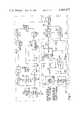
- FIG. 2there is shown a more detailed combined block and logic diagram of the invention which will be discussed with the aid of the timing waveforms of FIGS. 3 and 4.
- the timing waveformswill be referred to herein as waveforms 3A, 3B, 3C, etc. or waveforms 4A, 4B, etc. rather than as waveform A of FIG. 3 or waveform B of FIG. 4.
- the waveforms of FIG. 3which represent signals at various points in the structure of FIG. 2, are identified by encircled legends in FIG. 2 which correspond to the designations of the waveforms of FIG. 3.
- the encircled legend "3A"appearing at the output of clock source 200 of FIG. 2 and indicates that the signal represented by waveform 3A appears at that point.
- the logic within dashed line block 148corresponds to the logic within dashed line block 148 of FIG. 1.
- the remaining logic of FIG. 2corresponds to the logic within the dashed line block 146 of FIG. 1 but is shown in considerably more detail.
- the ROM 136 of FIG. 1is, in fact, the three ROM's 230, 218 and 220 of FIG. 2 with ROM's 218 and 220 being employed in the start mode of the system, and ROM 230 being employed during the steady state or run mode.
- the timing portion within block 142 of FIG. 1includes, in FIG. 2, clock source 200, divider 202, and counters 206, 204, 232 and 236.
- Frequency control latch 128a and latch 130 of FIG. 2together correspond to frequency control latch 128 of FIG. 1 and data symbol latch 140 of FIG. 1 corresponds to data symbol latch 140 of FIG. 2.
- a start pulse 231sets flip-flop 216 and resets flip-flop 226 (waveforms 3F and 3H) at time t 0 .
- the setting of flip-flop 216enables counters 204 and 206, ROMS 218 and 220 (waveform 3H), latch 130, and threshold detector 228.
- the resetting of flip-flop 226 at time t 0 in waveform 3Fdisables AND gates 244 and 248 and permits counters 206 and 204 to continue to run freely, as indicated in waveforms 3I, 3E, and 3D.
- the subsequent setting of flip-flop 226 at time t 1will reset counters 206 and 204 to 0 count for purposes that will become clearer later herein.
- the output from clock source 200(waveform 3A) is divided by two in divider 202 to produce a 2 5 ⁇ 9.6 KHz signal (waveform 3B) which is supplied to the clock input of 0--31 count counter 204.
- Counter 204will iteratively count through its 32 count capacity supplying each count of 0 (waveform 3D) to the clock input 208 of counter 206 and will also supply its actual count values to decoder 214 which will in turn supply the decoded count values to ROMS 218 and 220 to access the 32 word locations of said ROMS in successive order and supply the contents thereof, respectively, to OR gate 242 and to frequency control latch 128.
- the contents of the 32 word locations of ROM 218are the 32 correction PRS codes whose patterns are similar to the predetermined received PRS code mentioned above but whose frequencies are offset by varying amounts to cover the spectrum of frequencies of any expected Doppler shift in the predetermined received PRS code.
- These offset frequency correction PRS codesare employed to obtain synchronization of the system in the start mode and are comprised of I and Q components.
- Such offset correction PRS codesare supplied through OR gate 242 to the second input terminals 251 and 253 of I and Q correlators 116 and 118.
- Such 32 offset correction PRS codesare repeatedly supplied to I and Q correlators 116 and 118 during each chip period of the received PRS signal from signal source 100. This recirculation of the 32 offset correction PRS codes will continue until the predetermined received PRS code is supplied from signal source 100 to receiver 102. As the predetermined received PRS code begins to fill up the 64 stages of I and Q correlators 116 and 118 correlation pulses of increasing magnitude will be generated each time the corresponding offset correction PRS code is entered into correlators 116 and 118. The summed output of the correlation pulses, as they begin to occur, are supplied from summer 124 to A/D converter 126 and then to threshold detector 228 from summer 124.
- flip-flop 226When one of such correlation pulses (waveform 3C) exceeds a certain magnitude, as determined by threshold detector 228, flip-flop 226 is set to prime AND gate 244 and also to reset counters 204 and 206 to 0. The resetting of counters 204 and 206 to 0 enables the comparison (correlation) of the 32 offset correction PRS code signals with the received PRS code during the next 64 chip periods of said incoming PRS code, thereby assuring that said 32 offset correction PRS codes will, in fact, at some point during the following 64 input chip periods, be compared with the predetermined received PRS code when it is completely entered into the I and Q correlators 116 and 118, thereby providing maximum correlation.
- AND gate 244is primed so that when a pulse appears at the output of comparator 134 frequency control latch 128a is enabled to receive and store the contents of that memory location of ROM 220 which is being accessed at the time the pulse from comparator 134 occurs.
- the contents of the 32 memory locations of ROM 220are values which, when supplied to local oscillator 110, will alter the frequency of said local oscillator 110 by an amount equal to the offset frequency of that correction PRS code of the corresponding word location of memory ROM 218 which is causing the output signal from comparator 134.
- Worded in another mannereach time a correction PRS signal accessed in ROM 218 and supplied to I and Q correlators 116 and 118 produces a correlation pulse larger than the last largest one stored in amplitude latch 132 the output signal produced by comparator 134 will enable frequency control latch 128a through AND gate 244 to supply the value in the corresponding word location of ROM 220 to control latch 128a.
- the frequency control latch 128awill contain the value supplied from ROM 220 which represents the frequency error in the received signal.
- flip-flop 216At the end of the start mode flip-flop 216 is reset as discussed above and as shown in waveforms 3J at time t 2 .
- the resetting of flip-flop 216enables latch 130 to receive and store the contents of frequency control latch 128a, thereby finally implementing the required change in frequency of local oscillator 110 to compensate for the frequency error.
- Resetting of flip-flop 216also functions to disable ROM 218, enable ROM 230, and disable counters 204 and 206, and also threshold detector 228.
- the start mode of the systemhas now been completely disabled and will remain so until another start pulse 231 is supplied to the system.
- Enabling of ROM 230permits the contents of the 64 memory locations therein to be supplied through OR gate 242 to I and Q correlators 116 and 118. As discussed above, the 64 memory locations of ROM 230 contain the 64 possible received PRS codes although they are referred to as reference PRS codes herein.
- the count value output 0-63 of counter 232provides addresses to the 64 word locations in ROM 230.
- addresses of the word locations of ROM 230which addresses are the count value output of counter 232, are, in fact the data symbols corresponding individually to the 64 reference PRS codes stored in ROM 230.
- Each count of zero of counter 232is supplied to receiver 102 and is, in fact, the 9600 Hz sample rate of the signal received from source 100. Since counter 232 has the capacity of 64 counts it is apparent that all of the 64 reference PRS codes stored in ROM 230 will be completely recirculated through correlators 116 and 118 during each chip period of the received signal from source 100.
- each count of counter 232(waveform 4A) is also supplied to 0-63 counter 236 which was reset to 0 when flip-flop 216 was reset.
- the counter 236will count through its capacity to the count of 63 (waveform 4B) when it will read the contents of data symbol latch 140 into utilization means 240 (waveform 4D).
- data symbol latch 140each time the output of summer 124 produces a correlation signal larger than the one stored in amplitude latch 132, the comparator 134 will detect that the newly generated correlation pulse is greater than the stored one, and will output a signal on lead 139 (waveform 4C) to cause latch 132 to store the newly generated correlation signal. Such signal on lead 139 will also cause the data symbol latch 140, when switch 153 is closed, to store the address for ROM 230 which caused the new largest correlation pulse to be generated at the output of summer 124. Thus, data symbol latch 140 will always contain the address code word for the reference PRS signal which generated the last largest correlation pulse.
- the largest correlation pulseswill occur each time the corresponding reference PRS code is entered into correlators 116 and 118 and as the received PRS code becomes more fully entered into correlators 116 and 118.
- the correlation pulses 133 and 135are caused by the 23rd reference PRS code, arbitrarily selected, each time it appears in the correlators 116 and 118.
- the data symbol latch 140At the end of the 64 chip periods of the received signal defined by the output of counter 236 the data symbol latch 140 will contain the 6-bit address code for the reference PRS signal which generated the largest correlation pulse during the 64 chip periods of the received signal. Then at the trailing edge of the count of 63 of counter 236 the contents of data symbol latch 140 will be supplied to utilization means 240, as shown in waveform 4D.
Landscapes
- Engineering & Computer Science (AREA)
- Computer Networks & Wireless Communication (AREA)
- Signal Processing (AREA)
- Synchronisation In Digital Transmission Systems (AREA)
Abstract
Description
Claims (5)
Priority Applications (1)
| Application Number | Priority Date | Filing Date | Title |
|---|---|---|---|
| US06/399,879US4485477A (en) | 1982-07-19 | 1982-07-19 | Fast frequency/code search |
Applications Claiming Priority (1)
| Application Number | Priority Date | Filing Date | Title |
|---|---|---|---|
| US06/399,879US4485477A (en) | 1982-07-19 | 1982-07-19 | Fast frequency/code search |
Publications (1)
| Publication Number | Publication Date |
|---|---|
| US4485477Atrue US4485477A (en) | 1984-11-27 |
Family
ID=23581335
Family Applications (1)
| Application Number | Title | Priority Date | Filing Date |
|---|---|---|---|
| US06/399,879Expired - LifetimeUS4485477A (en) | 1982-07-19 | 1982-07-19 | Fast frequency/code search |
Country Status (1)
| Country | Link |
|---|---|
| US (1) | US4485477A (en) |
Cited By (38)
| Publication number | Priority date | Publication date | Assignee | Title |
|---|---|---|---|---|
| US4554672A (en)* | 1983-02-21 | 1985-11-19 | Nippon Telegraph & Telephone Public Corp. | Phase and frequency variable oscillator |
| US4601005A (en)* | 1981-12-31 | 1986-07-15 | The Secretary Of State For Defence In Her Britannic Majesty's Government Of The United Kingdom Of Great Britain And Northern Ireland | Receivers for navigation satellite systems |
| US4630283A (en)* | 1985-07-17 | 1986-12-16 | Rca Corporation | Fast acquisition burst mode spread spectrum communications system with pilot carrier |
| US4653076A (en)* | 1984-03-23 | 1987-03-24 | Sangamo Weston, Inc. | Timing signal correction system for use in direct sequence spread signal receiver |
| US4672629A (en)* | 1984-07-23 | 1987-06-09 | Standard Elektrik Lorenz Aktiengesellschaft | Receiver for bandspread signals |
| US4754465A (en)* | 1984-05-07 | 1988-06-28 | Trimble Navigation, Inc. | Global positioning system course acquisition code receiver |
| US4761795A (en)* | 1986-01-21 | 1988-08-02 | Standard Elektrik Lorenz Ag | Receiver for bandspread signals |
| US4847862A (en)* | 1988-04-07 | 1989-07-11 | Trimble Navigation, Ltd. | Global positioning system course acquisition code receiver |
| US4888788A (en)* | 1986-11-20 | 1989-12-19 | Matsushita Electric Industrial Co., Ltd. | Transmitting and receiving systems |
| US4908837A (en)* | 1987-08-04 | 1990-03-13 | Clarion Co., Ltd. | Receiver for spread spectrum communication |
| US4947409A (en)* | 1987-11-27 | 1990-08-07 | Telefonaktiebolaget L M Ericsson | Apparatus for correcting frequency in a coherent receiver |
| US5014066A (en)* | 1982-03-01 | 1991-05-07 | Western Atlas International, Inc. | System for simultaneously deriving position information from a plurality of satellite transmissions |
| US5081652A (en)* | 1989-05-31 | 1992-01-14 | Technophone Ltd. | Offset correction |
| US5090028A (en)* | 1989-07-28 | 1992-02-18 | U.S. Philips Corporation | Method of and apparatus for synchronization by means of correlation |
| US5132985A (en)* | 1990-07-04 | 1992-07-21 | Clarion Co., Ltd. | Spread spectrum receiver |
| US5148451A (en)* | 1989-11-10 | 1992-09-15 | Nec Corporation | Carrier regeneration device correctly operable in mobile satellite communication |
| US5230076A (en)* | 1984-10-30 | 1993-07-20 | The Secretary Of State For Defence In Her Britannic Majesty's Government Of The United Kingdom Of Great Britain And Northern Ireland | Ionospheric sounding |
| US5237587A (en)* | 1992-11-20 | 1993-08-17 | Magnavox Electronic Systems Company | Pseudo-noise modem and related digital correlation method |
| US5255290A (en)* | 1992-08-21 | 1993-10-19 | Teknekron Communications System, Inc. | Method and apparatus for combined frequency offset and timing offset estimation |
| US5267260A (en)* | 1992-11-19 | 1993-11-30 | Samsung Electronics Co., Ltd. | Spread spectrum receiver using the code division multiple access mode |
| US5276710A (en)* | 1991-07-30 | 1994-01-04 | Nec Corporation | Carrier frequency error detector capable of accurately detecting a carrier frequency error |
| US5303257A (en)* | 1992-12-31 | 1994-04-12 | Gte Government Systems Corporation | Carrier frequency correction for a DSSS communication system |
| US5329546A (en)* | 1992-11-27 | 1994-07-12 | Samsung Electronics Co., Ltd. | Clock recovery stabilization method and circuit in a receiver of a code division multiple access/direct sequence (CDMA/DS) system |
| US5509034A (en)* | 1994-02-14 | 1996-04-16 | Beukema; Troy J. | Frequency synchronizing method for a reference oscillator |
| WO1996041425A3 (en)* | 1995-06-07 | 1997-02-20 | Sanconix Inc | Direct sequence frequency ambiguity resolving receiver |
| US5619212A (en)* | 1982-03-01 | 1997-04-08 | Western Atlas International, Inc. | System for determining position from suppressed carrier radio waves |
| US5726974A (en)* | 1995-06-20 | 1998-03-10 | Matsushita Electric Industrial Co., Ltd. | Receiving circuit having a frequency compensated local oscillation circuit |
| US5812591A (en)* | 1994-09-23 | 1998-09-22 | Garmin Corporation | Dual conversion GPS frequency converter and frequency plan for same |
| US5943329A (en)* | 1995-09-11 | 1999-08-24 | Hitachi, Ltd. | Code division multiple access mobile communication system |
| US6005889A (en)* | 1997-07-17 | 1999-12-21 | Nokia | Pseudo-random noise detector for signals having a carrier frequency offset |
| US6195343B1 (en)* | 1996-03-15 | 2001-02-27 | Matsushita Electric Industrial Co., Ltd. | Spectrum spread communication system |
| US6765895B1 (en) | 1996-03-15 | 2004-07-20 | Matsushita Electric Industrial Co., Ltd. | Spectrum spread communication system |
| US20070046536A1 (en)* | 2005-08-31 | 2007-03-01 | Zhike Jia | Fast fourier transform with down sampling based navigational satellite signal tracking |
| US7545854B1 (en)* | 1998-09-01 | 2009-06-09 | Sirf Technology, Inc. | Doppler corrected spread spectrum matched filter |
| US7711038B1 (en) | 1998-09-01 | 2010-05-04 | Sirf Technology, Inc. | System and method for despreading in a spread spectrum matched filter |
| US7908080B2 (en) | 2004-12-31 | 2011-03-15 | Google Inc. | Transportation routing |
| US20200044687A1 (en)* | 2017-04-11 | 2020-02-06 | Fraunhofer-Gesellschaft zur Förderung der angewandten Forschung e.V | Specific hopping patterns for telegram splitting |
| CN114372307A (en)* | 2021-12-30 | 2022-04-19 | 国网江苏省电力工程咨询有限公司 | Construction management system and method for power substation based on BIM + GIS technology |
Citations (4)
| Publication number | Priority date | Publication date | Assignee | Title |
|---|---|---|---|---|
| US3868686A (en)* | 1973-04-16 | 1975-02-25 | Us Navy | Range tracking device for a portable attack warning radar |
| US4042925A (en)* | 1975-11-24 | 1977-08-16 | International Telephone And Telegraph Corporation | Pseudo-random code (PRC) surveilance radar |
| US4328588A (en)* | 1980-07-17 | 1982-05-04 | Rockwell International Corporation | Synchronization system for digital data |
| US4418393A (en)* | 1980-10-27 | 1983-11-29 | Sperry Corporation | Matched filter spread spectrum code recovery apparatus |
- 1982
- 1982-07-19USUS06/399,879patent/US4485477A/ennot_activeExpired - Lifetime
Patent Citations (4)
| Publication number | Priority date | Publication date | Assignee | Title |
|---|---|---|---|---|
| US3868686A (en)* | 1973-04-16 | 1975-02-25 | Us Navy | Range tracking device for a portable attack warning radar |
| US4042925A (en)* | 1975-11-24 | 1977-08-16 | International Telephone And Telegraph Corporation | Pseudo-random code (PRC) surveilance radar |
| US4328588A (en)* | 1980-07-17 | 1982-05-04 | Rockwell International Corporation | Synchronization system for digital data |
| US4418393A (en)* | 1980-10-27 | 1983-11-29 | Sperry Corporation | Matched filter spread spectrum code recovery apparatus |
Cited By (54)
| Publication number | Priority date | Publication date | Assignee | Title |
|---|---|---|---|---|
| US4601005A (en)* | 1981-12-31 | 1986-07-15 | The Secretary Of State For Defence In Her Britannic Majesty's Government Of The United Kingdom Of Great Britain And Northern Ireland | Receivers for navigation satellite systems |
| US5014066A (en)* | 1982-03-01 | 1991-05-07 | Western Atlas International, Inc. | System for simultaneously deriving position information from a plurality of satellite transmissions |
| US5619212A (en)* | 1982-03-01 | 1997-04-08 | Western Atlas International, Inc. | System for determining position from suppressed carrier radio waves |
| US5805200A (en)* | 1982-03-01 | 1998-09-08 | Western Atlas International, Inc. | System for determining position from pseudorandomly modulated radio signals |
| US4554672A (en)* | 1983-02-21 | 1985-11-19 | Nippon Telegraph & Telephone Public Corp. | Phase and frequency variable oscillator |
| US4653076A (en)* | 1984-03-23 | 1987-03-24 | Sangamo Weston, Inc. | Timing signal correction system for use in direct sequence spread signal receiver |
| US4754465A (en)* | 1984-05-07 | 1988-06-28 | Trimble Navigation, Inc. | Global positioning system course acquisition code receiver |
| US4672629A (en)* | 1984-07-23 | 1987-06-09 | Standard Elektrik Lorenz Aktiengesellschaft | Receiver for bandspread signals |
| US5230076A (en)* | 1984-10-30 | 1993-07-20 | The Secretary Of State For Defence In Her Britannic Majesty's Government Of The United Kingdom Of Great Britain And Northern Ireland | Ionospheric sounding |
| US4630283A (en)* | 1985-07-17 | 1986-12-16 | Rca Corporation | Fast acquisition burst mode spread spectrum communications system with pilot carrier |
| US4761795A (en)* | 1986-01-21 | 1988-08-02 | Standard Elektrik Lorenz Ag | Receiver for bandspread signals |
| US4888788A (en)* | 1986-11-20 | 1989-12-19 | Matsushita Electric Industrial Co., Ltd. | Transmitting and receiving systems |
| US4908837A (en)* | 1987-08-04 | 1990-03-13 | Clarion Co., Ltd. | Receiver for spread spectrum communication |
| US4947409A (en)* | 1987-11-27 | 1990-08-07 | Telefonaktiebolaget L M Ericsson | Apparatus for correcting frequency in a coherent receiver |
| US4847862A (en)* | 1988-04-07 | 1989-07-11 | Trimble Navigation, Ltd. | Global positioning system course acquisition code receiver |
| US5081652A (en)* | 1989-05-31 | 1992-01-14 | Technophone Ltd. | Offset correction |
| US5090028A (en)* | 1989-07-28 | 1992-02-18 | U.S. Philips Corporation | Method of and apparatus for synchronization by means of correlation |
| US5148451A (en)* | 1989-11-10 | 1992-09-15 | Nec Corporation | Carrier regeneration device correctly operable in mobile satellite communication |
| US5132985A (en)* | 1990-07-04 | 1992-07-21 | Clarion Co., Ltd. | Spread spectrum receiver |
| US5276710A (en)* | 1991-07-30 | 1994-01-04 | Nec Corporation | Carrier frequency error detector capable of accurately detecting a carrier frequency error |
| US5255290A (en)* | 1992-08-21 | 1993-10-19 | Teknekron Communications System, Inc. | Method and apparatus for combined frequency offset and timing offset estimation |
| US5267260A (en)* | 1992-11-19 | 1993-11-30 | Samsung Electronics Co., Ltd. | Spread spectrum receiver using the code division multiple access mode |
| US5237587A (en)* | 1992-11-20 | 1993-08-17 | Magnavox Electronic Systems Company | Pseudo-noise modem and related digital correlation method |
| US5329546A (en)* | 1992-11-27 | 1994-07-12 | Samsung Electronics Co., Ltd. | Clock recovery stabilization method and circuit in a receiver of a code division multiple access/direct sequence (CDMA/DS) system |
| US5303257A (en)* | 1992-12-31 | 1994-04-12 | Gte Government Systems Corporation | Carrier frequency correction for a DSSS communication system |
| US5509034A (en)* | 1994-02-14 | 1996-04-16 | Beukema; Troy J. | Frequency synchronizing method for a reference oscillator |
| US5812591A (en)* | 1994-09-23 | 1998-09-22 | Garmin Corporation | Dual conversion GPS frequency converter and frequency plan for same |
| WO1996041425A3 (en)* | 1995-06-07 | 1997-02-20 | Sanconix Inc | Direct sequence frequency ambiguity resolving receiver |
| US6111911A (en)* | 1995-06-07 | 2000-08-29 | Sanconix, Inc | Direct sequence frequency ambiguity resolving receiver |
| US5726974A (en)* | 1995-06-20 | 1998-03-10 | Matsushita Electric Industrial Co., Ltd. | Receiving circuit having a frequency compensated local oscillation circuit |
| US6721296B2 (en) | 1995-09-11 | 2004-04-13 | Hitachi, Ltd. | Code division multiple access mobile communication system |
| US7336697B2 (en) | 1995-09-11 | 2008-02-26 | Hitachi, Ltd. | Code division multiple access mobile communication system |
| US6292477B1 (en) | 1995-09-11 | 2001-09-18 | Hitachi, Ltd. | Code division multiple access mobile communication system |
| US6456609B2 (en) | 1995-09-11 | 2002-09-24 | Hitachi, Ltd. | Code division multiple access mobile communication system |
| US5943329A (en)* | 1995-09-11 | 1999-08-24 | Hitachi, Ltd. | Code division multiple access mobile communication system |
| US20040165651A1 (en)* | 1995-09-11 | 2004-08-26 | Yasuo Ohgoshi | Code division multiple access mobile communication system |
| US6195343B1 (en)* | 1996-03-15 | 2001-02-27 | Matsushita Electric Industrial Co., Ltd. | Spectrum spread communication system |
| US6765895B1 (en) | 1996-03-15 | 2004-07-20 | Matsushita Electric Industrial Co., Ltd. | Spectrum spread communication system |
| US6005889A (en)* | 1997-07-17 | 1999-12-21 | Nokia | Pseudo-random noise detector for signals having a carrier frequency offset |
| US7711038B1 (en) | 1998-09-01 | 2010-05-04 | Sirf Technology, Inc. | System and method for despreading in a spread spectrum matched filter |
| US7852905B2 (en) | 1998-09-01 | 2010-12-14 | Sirf Technology, Inc. | System and method for despreading in a spread spectrum matched filter |
| US7545854B1 (en)* | 1998-09-01 | 2009-06-09 | Sirf Technology, Inc. | Doppler corrected spread spectrum matched filter |
| US8798917B2 (en) | 2004-12-31 | 2014-08-05 | Google Inc. | Transportation routing |
| US7908080B2 (en) | 2004-12-31 | 2011-03-15 | Google Inc. | Transportation routing |
| US8606514B2 (en) | 2004-12-31 | 2013-12-10 | Google Inc. | Transportation routing |
| US9709415B2 (en) | 2004-12-31 | 2017-07-18 | Google Inc. | Transportation routing |
| US9778055B2 (en) | 2004-12-31 | 2017-10-03 | Google Inc. | Transportation routing |
| US9945686B2 (en) | 2004-12-31 | 2018-04-17 | Google Llc | Transportation routing |
| US11092455B2 (en) | 2004-12-31 | 2021-08-17 | Google Llc | Transportation routing |
| US8466836B2 (en)* | 2005-08-31 | 2013-06-18 | CSR Technology Holdings Inc. | Fast fourier transform with down sampling based navigational satellite signal tracking |
| US20070046536A1 (en)* | 2005-08-31 | 2007-03-01 | Zhike Jia | Fast fourier transform with down sampling based navigational satellite signal tracking |
| US20200044687A1 (en)* | 2017-04-11 | 2020-02-06 | Fraunhofer-Gesellschaft zur Förderung der angewandten Forschung e.V | Specific hopping patterns for telegram splitting |
| US11742893B2 (en)* | 2017-04-11 | 2023-08-29 | Fraunhofer-Gesellschaft zur Förderung der Angewandten Forschung, E.V. | Specific hopping patterns for telegram splitting |
| CN114372307A (en)* | 2021-12-30 | 2022-04-19 | 国网江苏省电力工程咨询有限公司 | Construction management system and method for power substation based on BIM + GIS technology |
Similar Documents
| Publication | Publication Date | Title |
|---|---|---|
| US4485477A (en) | Fast frequency/code search | |
| US4527275A (en) | Correlation data communications system | |
| US4477912A (en) | Correlation data communications system | |
| US5132986A (en) | Csk communication system | |
| US5396515A (en) | Asymmetric spread spectrum correlator | |
| KR100201798B1 (en) | Spread spectrum correlator | |
| US4347616A (en) | Digital multi-level multi-phase modulation communication system | |
| US3980825A (en) | System for the transmission of split-phase Manchester coded bivalent information signals | |
| US5864585A (en) | Cosine segment communications system | |
| US4290140A (en) | Combined coherent frequency and phase shift keying modulation system | |
| US5090028A (en) | Method of and apparatus for synchronization by means of correlation | |
| KR100301407B1 (en) | Manchester - Modulated FM signal modulator | |
| EP0540664A4 (en) | Sawc phase-detection method and apparatus | |
| KR100470000B1 (en) | FREQUENCY TRACKING FOR COMMUNICATION SIGNALS USING M-ary ORTHOGONAL WALSH MODULATION | |
| EP0119008A2 (en) | Improved coherent phase shift keyed demodulator for power line communication systems | |
| US5031192A (en) | Synthetic demodulation of spread spectrum signals | |
| US4276650A (en) | Method of synchronizing a quadphase receiver and clock synchronization device for carrying out the method | |
| US4652838A (en) | Phase randomization to reduce detectability of phase or frequency-modulated digital signals | |
| US7221696B1 (en) | Communication system and method for acquiring pseudonoise codes or carrier signals under conditions of relatively large chip rate uncertainty | |
| US4352194A (en) | System and method for frequency discrimination | |
| US6700940B1 (en) | Carrier reproduction circuit | |
| US4412302A (en) | Digital phase demodulation and correlation | |
| JP3278311B2 (en) | Data transceiver | |
| KR100280044B1 (en) | Receiver in Direct Diffusion System | |
| SU1573550A1 (en) | Device for transmission and reception of discrete messages |
Legal Events
| Date | Code | Title | Description |
|---|---|---|---|
| AS | Assignment | Owner name:RCA CORPORATION A CORP OF DE Free format text:ASSIGNMENT OF ASSIGNORS INTEREST.;ASSIGNOR:NOSSEN, EDWARD J.;REEL/FRAME:004026/0877 Effective date:19820708 | |
| STCF | Information on status: patent grant | Free format text:PATENTED CASE | |
| FPAY | Fee payment | Year of fee payment:4 | |
| FPAY | Fee payment | Year of fee payment:8 | |
| AS | Assignment | Owner name:MARTIN MARIETTA CORPORATION, MARYLAND Free format text:ASSIGNMENT OF ASSIGNORS INTEREST;ASSIGNOR:GENERAL ELECTRIC COMPANY;REEL/FRAME:007046/0736 Effective date:19940322 | |
| FPAY | Fee payment | Year of fee payment:12 | |
| AS | Assignment | Owner name:LOCKHEED MARTIN CORPORATION, MARYLAND Free format text:ASSIGNMENT OF ASSIGNORS INTEREST;ASSIGNOR:MARTIN MARIETTA CORPORATION;REEL/FRAME:008628/0518 Effective date:19960128 | |
| AS | Assignment | Owner name:L-3 COMMUNICATIONS CORPORATION, NEW YORK Free format text:ASSIGNMENT OF ASSIGNORS INTEREST;ASSIGNOR:LOCKHEED MARTIN CORPORATION, A CORP. OF MD;REEL/FRAME:010180/0073 Effective date:19970430 |