US4484143A - CCD Demodulator circuit - Google Patents
CCD Demodulator circuitDownload PDFInfo
- Publication number
- US4484143A US4484143AUS06/448,570US44857082AUS4484143AUS 4484143 AUS4484143 AUS 4484143AUS 44857082 AUS44857082 AUS 44857082AUS 4484143 AUS4484143 AUS 4484143A
- Authority
- US
- United States
- Prior art keywords
- output
- signal
- gate
- input
- carrier signal
- Prior art date
- Legal status (The legal status is an assumption and is not a legal conclusion. Google has not performed a legal analysis and makes no representation as to the accuracy of the status listed.)
- Expired - Lifetime
Links
- 238000012545processingMethods0.000claimsdescription5
- 230000005540biological transmissionEffects0.000claimsdescription4
- 239000004065semiconductorSubstances0.000abstractdescription54
- 230000005669field effectEffects0.000abstractdescription8
- 238000005516engineering processMethods0.000abstractdescription4
- 238000005070samplingMethods0.000abstract2
- 238000010586diagramMethods0.000description24
- 238000009792diffusion processMethods0.000description14
- 238000012546transferMethods0.000description14
- 239000000758substrateSubstances0.000description9
- 239000002019doping agentSubstances0.000description4
- 229910021420polycrystalline siliconInorganic materials0.000description4
- 229920005591polysiliconPolymers0.000description4
- XUIMIQQOPSSXEZ-UHFFFAOYSA-NSiliconChemical compound[Si]XUIMIQQOPSSXEZ-UHFFFAOYSA-N0.000description3
- XAGFODPZIPBFFR-UHFFFAOYSA-NaluminiumChemical compound[Al]XAGFODPZIPBFFR-UHFFFAOYSA-N0.000description3
- 229910052782aluminiumInorganic materials0.000description3
- 239000000463materialSubstances0.000description3
- 229910052710siliconInorganic materials0.000description3
- 239000010703siliconSubstances0.000description3
- VYPSYNLAJGMNEJ-UHFFFAOYSA-NSilicium dioxideChemical compoundO=[Si]=OVYPSYNLAJGMNEJ-UHFFFAOYSA-N0.000description2
- 238000000034methodMethods0.000description2
- 230000006978adaptationEffects0.000description1
- 238000005513bias potentialMethods0.000description1
- 230000008859changeEffects0.000description1
- 150000001875compoundsChemical class0.000description1
- 238000010276constructionMethods0.000description1
- 238000001514detection methodMethods0.000description1
- 238000011982device technologyMethods0.000description1
- 239000012777electrically insulating materialSubstances0.000description1
- 238000011067equilibrationMethods0.000description1
- 238000012986modificationMethods0.000description1
- 230000004048modificationEffects0.000description1
- 229910021421monocrystalline siliconInorganic materials0.000description1
- 230000035515penetrationEffects0.000description1
- 238000005036potential barrierMethods0.000description1
- 235000012239silicon dioxideNutrition0.000description1
- 239000000377silicon dioxideSubstances0.000description1
- 230000003068static effectEffects0.000description1
Images


Classifications
- H—ELECTRICITY
- H03—ELECTRONIC CIRCUITRY
- H03D—DEMODULATION OR TRANSFERENCE OF MODULATION FROM ONE CARRIER TO ANOTHER
- H03D1/00—Demodulation of amplitude-modulated oscillations
- H03D1/22—Homodyne or synchrodyne circuits
- G—PHYSICS
- G11—INFORMATION STORAGE
- G11C—STATIC STORES
- G11C27/00—Electric analogue stores, e.g. for storing instantaneous values
- G11C27/04—Shift registers
- H—ELECTRICITY
- H03—ELECTRONIC CIRCUITRY
- H03D—DEMODULATION OR TRANSFERENCE OF MODULATION FROM ONE CARRIER TO ANOTHER
- H03D13/00—Circuits for comparing the phase or frequency of two mutually-independent oscillations
- H—ELECTRICITY
- H10—SEMICONDUCTOR DEVICES; ELECTRIC SOLID-STATE DEVICES NOT OTHERWISE PROVIDED FOR
- H10D—INORGANIC ELECTRIC SEMICONDUCTOR DEVICES
- H10D30/00—Field-effect transistors [FET]
- H10D30/60—Insulated-gate field-effect transistors [IGFET]
- H—ELECTRICITY
- H10—SEMICONDUCTOR DEVICES; ELECTRIC SOLID-STATE DEVICES NOT OTHERWISE PROVIDED FOR
- H10D—INORGANIC ELECTRIC SEMICONDUCTOR DEVICES
- H10D44/00—Charge transfer devices
- H10D44/40—Charge-coupled devices [CCD]
- H10D44/45—Charge-coupled devices [CCD] having field effect produced by insulated gate electrodes
- H10D44/452—Input structures
Definitions
- FIG. 2also shows the amplifier portion 13 of the circuit according to the present invention including a second semiconductor region 15 of a second conductivity type (i.e. n type) adjacent the major surface and extends from the surface to a predetermined depth into a body.
- the second semiconductor region 15is spaced from the first semiconductor region 14 and electrically isolated therefrom by the substrate 40.
- This second semiconductor region of second conductivity typefurther contains first and second spaced-apart semiconductor subregions 43 and 44 respectively of the same second conductivity type adjacent said major surface.
- the first and second subregionshave a second conductivity type forming dopant concentration higher than that of the second semiconductor region itself, such as having n+ type conductivity.
- Such first and second subregionsform the source and drain zones of a field effect transistor which is used as an amplifier for the output signal generated in the present circuit.
- a first signal line 32is physically and electrically connected to the first subregion 43 by means of the contact 33.
- a second signal line 34makes physical and electrical contact with the second subregion 44 by means of the contact 35.
- the source and drain electrodesmay therefore be connected to other elements of the circuit in order to further amplify or utilize the signal, as is known by those skilled in the art.
- a signal known as a reset gate (RG) signalis applied during a third subsequent time interval for the purpose of making the field effect transistor constituted by the subregions 42 and 46 and gate electrode 47 conductive so as to drain the charge located on the output gate 31 at an appropriate time, thereby "resetting" the storage gate to receive further charge from the input.
- a signal line 50is further provided which makes contact with the second subregion 46 at the contact 51, which functions to DC bias the amplifier gate during reset.
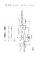
- FIG. 3bshows a sequence of four potential well diagrams taken at successive time interval t 0 , t 1 , t 2 , and t 3 , and two further potential well diagrams at a much later time during subsequent time intervals t N and t N+1 .
- the potential barrier under the gate G 1is seen to decrease from the period t 0 to t 1 and increase from the period t 2 to t 3 .
- the stored charge in the region under the gate G 2slowly begins to diffuse in the left hand direction.
- the potential underneath the gate G 1is at a potential level V 1
- the potential under the gate G 1is at a lower level.
- the level V INis the initial input voltage applied to the charge storage areas by means of the input line 16.
- the shaded portionrepresents charge storage in the semiconductor region between the subregions 41 and 42.
- the ⁇ 2 signal shown in FIG. 4 applied to the output transfer gateis defined by a waveform going from a relatively negative voltage level to a relatively positive level for a time internval of at least 100 ns. for a typical 6 ⁇ m gate dimension.
- the function of the output transfer gate signalis to transfer the charge stored in the region underneath G 2 into the semiconductor region 42 and thence onto the gate 31.
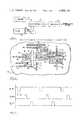
- FIG. 5is a timing diagram of the operation of the present invention in demodulating the applied radio frequency signal.
- the FIGURE's first waveformshows the typical amplitude modulated radio frequency signal that might be applied to the G 1 gate at frequency f.
- the second waveform shownis the sample pulse or the ⁇ 1 waveform. It is noted from the diagram that the sample frequency of ⁇ is much less than the frequency of the RF signal, so that the sample frequency undersamples the applied radio frequency signal.
- the thirdshows the output waveform produced by the present invention having as an input the radio frequency input signal shown in FIG. 4.
- the output signalrepresents the demodulation of the radio frequency signal shown above in FIG. 4.
- the output signal shown in FIG. 4is produced by a voltage or current variation of a signal in the conduction path of the field effect transistor defined by 43, 31, and 44 in FIG. 2.
- diode switch 60off, diode switch 61 on
- diode switch 60off, diode switch 61 off
- phase and amplitude modulated carrier signalis applied to the input of one of the diode switches, e.g. diode switch 60, and a reference signal applied to the other diode switch, e.g. diode switch 61.
- the diode switches 60 and 61are then sequentially switched on and off by the timing and bias circuit 63 so that the four possible output signals are generated.
- the output signalsare applied to the A/D converter 64 to produce digital signals which are applied to the microprocessor 65.
- the microprocessorproduces a multibit digital output representing the phase difference between the input signal and the reference signal.
Landscapes
- Engineering & Computer Science (AREA)
- Power Engineering (AREA)
- Solid State Image Pick-Up Elements (AREA)
Abstract
Description
Claims (3)
Priority Applications (1)
| Application Number | Priority Date | Filing Date | Title |
|---|---|---|---|
| US06/448,570US4484143A (en) | 1982-05-17 | 1982-12-10 | CCD Demodulator circuit |
Applications Claiming Priority (2)
| Application Number | Priority Date | Filing Date | Title |
|---|---|---|---|
| US06/379,244US4389615A (en) | 1979-08-29 | 1982-05-17 | CCD Demodulator circuit |
| US06/448,570US4484143A (en) | 1982-05-17 | 1982-12-10 | CCD Demodulator circuit |
Related Parent Applications (1)
| Application Number | Title | Priority Date | Filing Date |
|---|---|---|---|
| US06/379,244DivisionUS4389615A (en) | 1979-08-29 | 1982-05-17 | CCD Demodulator circuit |
Publications (1)
| Publication Number | Publication Date |
|---|---|
| US4484143Atrue US4484143A (en) | 1984-11-20 |
Family
ID=27008537
Family Applications (1)
| Application Number | Title | Priority Date | Filing Date |
|---|---|---|---|
| US06/448,570Expired - LifetimeUS4484143A (en) | 1982-05-17 | 1982-12-10 | CCD Demodulator circuit |
Country Status (1)
| Country | Link |
|---|---|
| US (1) | US4484143A (en) |
Cited By (40)
| Publication number | Priority date | Publication date | Assignee | Title |
|---|---|---|---|---|
| US5896061A (en)* | 1992-10-29 | 1999-04-20 | Sican Gesellschaft Fur Silizium-Anwendungen Und Cad/Cat | Homodyne receiver and process for correcting the converted received signal |
| WO2001047202A3 (en)* | 1999-12-22 | 2002-02-14 | Parkervision Inc | Phase comparator using undersampling |
| US6542722B1 (en) | 1998-10-21 | 2003-04-01 | Parkervision, Inc. | Method and system for frequency up-conversion with variety of transmitter configurations |
| US6560301B1 (en) | 1998-10-21 | 2003-05-06 | Parkervision, Inc. | Integrated frequency translation and selectivity with a variety of filter embodiments |
| US6580902B1 (en) | 1998-10-21 | 2003-06-17 | Parkervision, Inc. | Frequency translation using optimized switch structures |
| US6647250B1 (en) | 1998-10-21 | 2003-11-11 | Parkervision, Inc. | Method and system for ensuring reception of a communications signal |
| US6694128B1 (en) | 1998-08-18 | 2004-02-17 | Parkervision, Inc. | Frequency synthesizer using universal frequency translation technology |
| US6704549B1 (en) | 1999-03-03 | 2004-03-09 | Parkvision, Inc. | Multi-mode, multi-band communication system |
| US6704558B1 (en) | 1999-01-22 | 2004-03-09 | Parkervision, Inc. | Image-reject down-converter and embodiments thereof, such as the family radio service |
| US6798351B1 (en) | 1998-10-21 | 2004-09-28 | Parkervision, Inc. | Automated meter reader applications of universal frequency translation |
| US6813485B2 (en) | 1998-10-21 | 2004-11-02 | Parkervision, Inc. | Method and system for down-converting and up-converting an electromagnetic signal, and transforms for same |
| US6873836B1 (en) | 1999-03-03 | 2005-03-29 | Parkervision, Inc. | Universal platform module and methods and apparatuses relating thereto enabled by universal frequency translation technology |
| US6879817B1 (en) | 1999-04-16 | 2005-04-12 | Parkervision, Inc. | DC offset, re-radiation, and I/Q solutions using universal frequency translation technology |
| US6963734B2 (en) | 1999-12-22 | 2005-11-08 | Parkervision, Inc. | Differential frequency down-conversion using techniques of universal frequency translation technology |
| US6975848B2 (en) | 2002-06-04 | 2005-12-13 | Parkervision, Inc. | Method and apparatus for DC offset removal in a radio frequency communication channel |
| US7006805B1 (en) | 1999-01-22 | 2006-02-28 | Parker Vision, Inc. | Aliasing communication system with multi-mode and multi-band functionality and embodiments thereof, such as the family radio service |
| US7010286B2 (en) | 2000-04-14 | 2006-03-07 | Parkervision, Inc. | Apparatus, system, and method for down-converting and up-converting electromagnetic signals |
| US7010559B2 (en) | 2000-11-14 | 2006-03-07 | Parkervision, Inc. | Method and apparatus for a parallel correlator and applications thereof |
| US7027786B1 (en) | 1998-10-21 | 2006-04-11 | Parkervision, Inc. | Carrier and clock recovery using universal frequency translation |
| US7039372B1 (en) | 1998-10-21 | 2006-05-02 | Parkervision, Inc. | Method and system for frequency up-conversion with modulation embodiments |
| US7054296B1 (en) | 1999-08-04 | 2006-05-30 | Parkervision, Inc. | Wireless local area network (WLAN) technology and applications including techniques of universal frequency translation |
| US7072390B1 (en) | 1999-08-04 | 2006-07-04 | Parkervision, Inc. | Wireless local area network (WLAN) using universal frequency translation technology including multi-phase embodiments |
| US7072427B2 (en) | 2001-11-09 | 2006-07-04 | Parkervision, Inc. | Method and apparatus for reducing DC offsets in a communication system |
| US7082171B1 (en) | 1999-11-24 | 2006-07-25 | Parkervision, Inc. | Phase shifting applications of universal frequency translation |
| US7085335B2 (en) | 2001-11-09 | 2006-08-01 | Parkervision, Inc. | Method and apparatus for reducing DC offsets in a communication system |
| US7110435B1 (en) | 1999-03-15 | 2006-09-19 | Parkervision, Inc. | Spread spectrum applications of universal frequency translation |
| US7110444B1 (en) | 1999-08-04 | 2006-09-19 | Parkervision, Inc. | Wireless local area network (WLAN) using universal frequency translation technology including multi-phase embodiments and circuit implementations |
| US7236754B2 (en) | 1999-08-23 | 2007-06-26 | Parkervision, Inc. | Method and system for frequency up-conversion |
| US7292835B2 (en) | 2000-01-28 | 2007-11-06 | Parkervision, Inc. | Wireless and wired cable modem applications of universal frequency translation technology |
| US7295826B1 (en) | 1998-10-21 | 2007-11-13 | Parkervision, Inc. | Integrated frequency translation and selectivity with gain control functionality, and applications thereof |
| US7321640B2 (en) | 2002-06-07 | 2008-01-22 | Parkervision, Inc. | Active polyphase inverter filter for quadrature signal generation |
| US7379883B2 (en) | 2002-07-18 | 2008-05-27 | Parkervision, Inc. | Networking methods and systems |
| US7454453B2 (en) | 2000-11-14 | 2008-11-18 | Parkervision, Inc. | Methods, systems, and computer program products for parallel correlation and applications thereof |
| US7460584B2 (en) | 2002-07-18 | 2008-12-02 | Parkervision, Inc. | Networking methods and systems |
| US7515896B1 (en) | 1998-10-21 | 2009-04-07 | Parkervision, Inc. | Method and system for down-converting an electromagnetic signal, and transforms for same, and aperture relationships |
| US7554508B2 (en) | 2000-06-09 | 2009-06-30 | Parker Vision, Inc. | Phased array antenna applications on universal frequency translation |
| US7693230B2 (en) | 1999-04-16 | 2010-04-06 | Parkervision, Inc. | Apparatus and method of differential IQ frequency up-conversion |
| US7724845B2 (en) | 1999-04-16 | 2010-05-25 | Parkervision, Inc. | Method and system for down-converting and electromagnetic signal, and transforms for same |
| US7773688B2 (en) | 1999-04-16 | 2010-08-10 | Parkervision, Inc. | Method, system, and apparatus for balanced frequency up-conversion, including circuitry to directly couple the outputs of multiple transistors |
| US8295406B1 (en) | 1999-08-04 | 2012-10-23 | Parkervision, Inc. | Universal platform module for a plurality of communication protocols |
Citations (3)
| Publication number | Priority date | Publication date | Assignee | Title |
|---|---|---|---|---|
| US4253067A (en)* | 1978-12-11 | 1981-02-24 | Rockwell International Corporation | Baseband differentially phase encoded radio signal detector |
| US4292593A (en)* | 1979-03-26 | 1981-09-29 | U.S. Philips Corporation | Method of demodulating a quadphase coded data signal and receiver for carrying out the method |
| US4412181A (en)* | 1980-04-01 | 1983-10-25 | Thomson-Csf | Process for the demodulation of an amplitude modulated signal and demodulator performing this process |
- 1982
- 1982-12-10USUS06/448,570patent/US4484143A/ennot_activeExpired - Lifetime
Patent Citations (3)
| Publication number | Priority date | Publication date | Assignee | Title |
|---|---|---|---|---|
| US4253067A (en)* | 1978-12-11 | 1981-02-24 | Rockwell International Corporation | Baseband differentially phase encoded radio signal detector |
| US4292593A (en)* | 1979-03-26 | 1981-09-29 | U.S. Philips Corporation | Method of demodulating a quadphase coded data signal and receiver for carrying out the method |
| US4412181A (en)* | 1980-04-01 | 1983-10-25 | Thomson-Csf | Process for the demodulation of an amplitude modulated signal and demodulator performing this process |
Cited By (96)
| Publication number | Priority date | Publication date | Assignee | Title |
|---|---|---|---|---|
| US5896061A (en)* | 1992-10-29 | 1999-04-20 | Sican Gesellschaft Fur Silizium-Anwendungen Und Cad/Cat | Homodyne receiver and process for correcting the converted received signal |
| US6694128B1 (en) | 1998-08-18 | 2004-02-17 | Parkervision, Inc. | Frequency synthesizer using universal frequency translation technology |
| US7321735B1 (en) | 1998-10-21 | 2008-01-22 | Parkervision, Inc. | Optical down-converter using universal frequency translation technology |
| US7826817B2 (en) | 1998-10-21 | 2010-11-02 | Parker Vision, Inc. | Applications of universal frequency translation |
| US6580902B1 (en) | 1998-10-21 | 2003-06-17 | Parkervision, Inc. | Frequency translation using optimized switch structures |
| US6647250B1 (en) | 1998-10-21 | 2003-11-11 | Parkervision, Inc. | Method and system for ensuring reception of a communications signal |
| US6687493B1 (en) | 1998-10-21 | 2004-02-03 | Parkervision, Inc. | Method and circuit for down-converting a signal using a complementary FET structure for improved dynamic range |
| US6542722B1 (en) | 1998-10-21 | 2003-04-01 | Parkervision, Inc. | Method and system for frequency up-conversion with variety of transmitter configurations |
| US7308242B2 (en) | 1998-10-21 | 2007-12-11 | Parkervision, Inc. | Method and system for down-converting and up-converting an electromagnetic signal, and transforms for same |
| US7376410B2 (en) | 1998-10-21 | 2008-05-20 | Parkervision, Inc. | Methods and systems for down-converting a signal using a complementary transistor structure |
| US6798351B1 (en) | 1998-10-21 | 2004-09-28 | Parkervision, Inc. | Automated meter reader applications of universal frequency translation |
| US6813485B2 (en) | 1998-10-21 | 2004-11-02 | Parkervision, Inc. | Method and system for down-converting and up-converting an electromagnetic signal, and transforms for same |
| US6836650B2 (en) | 1998-10-21 | 2004-12-28 | Parkervision, Inc. | Methods and systems for down-converting electromagnetic signals, and applications thereof |
| US7245886B2 (en) | 1998-10-21 | 2007-07-17 | Parkervision, Inc. | Method and system for frequency up-conversion with modulation embodiments |
| US7620378B2 (en) | 1998-10-21 | 2009-11-17 | Parkervision, Inc. | Method and system for frequency up-conversion with modulation embodiments |
| US8340618B2 (en) | 1998-10-21 | 2012-12-25 | Parkervision, Inc. | Method and system for down-converting an electromagnetic signal, and transforms for same, and aperture relationships |
| US8233855B2 (en) | 1998-10-21 | 2012-07-31 | Parkervision, Inc. | Up-conversion based on gated information signal |
| US7936022B2 (en) | 1998-10-21 | 2011-05-03 | Parkervision, Inc. | Method and circuit for down-converting a signal |
| US7529522B2 (en) | 1998-10-21 | 2009-05-05 | Parkervision, Inc. | Apparatus and method for communicating an input signal in polar representation |
| US7515896B1 (en) | 1998-10-21 | 2009-04-07 | Parkervision, Inc. | Method and system for down-converting an electromagnetic signal, and transforms for same, and aperture relationships |
| US7016663B2 (en) | 1998-10-21 | 2006-03-21 | Parkervision, Inc. | Applications of universal frequency translation |
| US7027786B1 (en) | 1998-10-21 | 2006-04-11 | Parkervision, Inc. | Carrier and clock recovery using universal frequency translation |
| US7039372B1 (en) | 1998-10-21 | 2006-05-02 | Parkervision, Inc. | Method and system for frequency up-conversion with modulation embodiments |
| US7050508B2 (en) | 1998-10-21 | 2006-05-23 | Parkervision, Inc. | Method and system for frequency up-conversion with a variety of transmitter configurations |
| US7937059B2 (en) | 1998-10-21 | 2011-05-03 | Parkervision, Inc. | Converting an electromagnetic signal via sub-sampling |
| US7693502B2 (en) | 1998-10-21 | 2010-04-06 | Parkervision, Inc. | Method and system for down-converting an electromagnetic signal, transforms for same, and aperture relationships |
| US8190116B2 (en) | 1998-10-21 | 2012-05-29 | Parker Vision, Inc. | Methods and systems for down-converting a signal using a complementary transistor structure |
| US7076011B2 (en) | 1998-10-21 | 2006-07-11 | Parkervision, Inc. | Integrated frequency translation and selectivity |
| US8190108B2 (en) | 1998-10-21 | 2012-05-29 | Parkervision, Inc. | Method and system for frequency up-conversion |
| US8160534B2 (en) | 1998-10-21 | 2012-04-17 | Parkervision, Inc. | Applications of universal frequency translation |
| US6560301B1 (en) | 1998-10-21 | 2003-05-06 | Parkervision, Inc. | Integrated frequency translation and selectivity with a variety of filter embodiments |
| US7697916B2 (en) | 1998-10-21 | 2010-04-13 | Parkervision, Inc. | Applications of universal frequency translation |
| US7389100B2 (en) | 1998-10-21 | 2008-06-17 | Parkervision, Inc. | Method and circuit for down-converting a signal |
| US7295826B1 (en) | 1998-10-21 | 2007-11-13 | Parkervision, Inc. | Integrated frequency translation and selectivity with gain control functionality, and applications thereof |
| US7194246B2 (en) | 1998-10-21 | 2007-03-20 | Parkervision, Inc. | Methods and systems for down-converting a signal using a complementary transistor structure |
| US8019291B2 (en) | 1998-10-21 | 2011-09-13 | Parkervision, Inc. | Method and system for frequency down-conversion and frequency up-conversion |
| US7218907B2 (en) | 1998-10-21 | 2007-05-15 | Parkervision, Inc. | Method and circuit for down-converting a signal |
| US7865177B2 (en) | 1998-10-21 | 2011-01-04 | Parkervision, Inc. | Method and system for down-converting an electromagnetic signal, and transforms for same, and aperture relationships |
| US7006805B1 (en) | 1999-01-22 | 2006-02-28 | Parker Vision, Inc. | Aliasing communication system with multi-mode and multi-band functionality and embodiments thereof, such as the family radio service |
| US6704558B1 (en) | 1999-01-22 | 2004-03-09 | Parkervision, Inc. | Image-reject down-converter and embodiments thereof, such as the family radio service |
| US7483686B2 (en) | 1999-03-03 | 2009-01-27 | Parkervision, Inc. | Universal platform module and methods and apparatuses relating thereto enabled by universal frequency translation technology |
| US6873836B1 (en) | 1999-03-03 | 2005-03-29 | Parkervision, Inc. | Universal platform module and methods and apparatuses relating thereto enabled by universal frequency translation technology |
| US6704549B1 (en) | 1999-03-03 | 2004-03-09 | Parkvision, Inc. | Multi-mode, multi-band communication system |
| US7599421B2 (en) | 1999-03-15 | 2009-10-06 | Parkervision, Inc. | Spread spectrum applications of universal frequency translation |
| US7110435B1 (en) | 1999-03-15 | 2006-09-19 | Parkervision, Inc. | Spread spectrum applications of universal frequency translation |
| US8036304B2 (en) | 1999-04-16 | 2011-10-11 | Parkervision, Inc. | Apparatus and method of differential IQ frequency up-conversion |
| US7894789B2 (en) | 1999-04-16 | 2011-02-22 | Parkervision, Inc. | Down-conversion of an electromagnetic signal with feedback control |
| US7272164B2 (en) | 1999-04-16 | 2007-09-18 | Parkervision, Inc. | Reducing DC offsets using spectral spreading |
| US7224749B2 (en) | 1999-04-16 | 2007-05-29 | Parkervision, Inc. | Method and apparatus for reducing re-radiation using techniques of universal frequency translation technology |
| US7190941B2 (en) | 1999-04-16 | 2007-03-13 | Parkervision, Inc. | Method and apparatus for reducing DC offsets in communication systems using universal frequency translation technology |
| US7773688B2 (en) | 1999-04-16 | 2010-08-10 | Parkervision, Inc. | Method, system, and apparatus for balanced frequency up-conversion, including circuitry to directly couple the outputs of multiple transistors |
| US8077797B2 (en) | 1999-04-16 | 2011-12-13 | Parkervision, Inc. | Method, system, and apparatus for balanced frequency up-conversion of a baseband signal |
| US7724845B2 (en) | 1999-04-16 | 2010-05-25 | Parkervision, Inc. | Method and system for down-converting and electromagnetic signal, and transforms for same |
| US7929638B2 (en) | 1999-04-16 | 2011-04-19 | Parkervision, Inc. | Wireless local area network (WLAN) using universal frequency translation technology including multi-phase embodiments |
| US8223898B2 (en) | 1999-04-16 | 2012-07-17 | Parkervision, Inc. | Method and system for down-converting an electromagnetic signal, and transforms for same |
| US8594228B2 (en) | 1999-04-16 | 2013-11-26 | Parkervision, Inc. | Apparatus and method of differential IQ frequency up-conversion |
| US7693230B2 (en) | 1999-04-16 | 2010-04-06 | Parkervision, Inc. | Apparatus and method of differential IQ frequency up-conversion |
| US8224281B2 (en) | 1999-04-16 | 2012-07-17 | Parkervision, Inc. | Down-conversion of an electromagnetic signal with feedback control |
| US8229023B2 (en) | 1999-04-16 | 2012-07-24 | Parkervision, Inc. | Wireless local area network (WLAN) using universal frequency translation technology including multi-phase embodiments |
| US7539474B2 (en) | 1999-04-16 | 2009-05-26 | Parkervision, Inc. | DC offset, re-radiation, and I/Q solutions using universal frequency translation technology |
| US6879817B1 (en) | 1999-04-16 | 2005-04-12 | Parkervision, Inc. | DC offset, re-radiation, and I/Q solutions using universal frequency translation technology |
| US7054296B1 (en) | 1999-08-04 | 2006-05-30 | Parkervision, Inc. | Wireless local area network (WLAN) technology and applications including techniques of universal frequency translation |
| US7653145B2 (en) | 1999-08-04 | 2010-01-26 | Parkervision, Inc. | Wireless local area network (WLAN) using universal frequency translation technology including multi-phase embodiments and circuit implementations |
| US8295406B1 (en) | 1999-08-04 | 2012-10-23 | Parkervision, Inc. | Universal platform module for a plurality of communication protocols |
| US7072390B1 (en) | 1999-08-04 | 2006-07-04 | Parkervision, Inc. | Wireless local area network (WLAN) using universal frequency translation technology including multi-phase embodiments |
| US7110444B1 (en) | 1999-08-04 | 2006-09-19 | Parkervision, Inc. | Wireless local area network (WLAN) using universal frequency translation technology including multi-phase embodiments and circuit implementations |
| US7546096B2 (en) | 1999-08-23 | 2009-06-09 | Parkervision, Inc. | Frequency up-conversion using a harmonic generation and extraction module |
| US7236754B2 (en) | 1999-08-23 | 2007-06-26 | Parkervision, Inc. | Method and system for frequency up-conversion |
| US7082171B1 (en) | 1999-11-24 | 2006-07-25 | Parkervision, Inc. | Phase shifting applications of universal frequency translation |
| US7379515B2 (en) | 1999-11-24 | 2008-05-27 | Parkervision, Inc. | Phased array antenna applications of universal frequency translation |
| WO2001047202A3 (en)* | 1999-12-22 | 2002-02-14 | Parkervision Inc | Phase comparator using undersampling |
| US6963734B2 (en) | 1999-12-22 | 2005-11-08 | Parkervision, Inc. | Differential frequency down-conversion using techniques of universal frequency translation technology |
| US7292835B2 (en) | 2000-01-28 | 2007-11-06 | Parkervision, Inc. | Wireless and wired cable modem applications of universal frequency translation technology |
| US7386292B2 (en) | 2000-04-14 | 2008-06-10 | Parkervision, Inc. | Apparatus, system, and method for down-converting and up-converting electromagnetic signals |
| US7107028B2 (en) | 2000-04-14 | 2006-09-12 | Parkervision, Inc. | Apparatus, system, and method for up converting electromagnetic signals |
| US7496342B2 (en) | 2000-04-14 | 2009-02-24 | Parkervision, Inc. | Down-converting electromagnetic signals, including controlled discharge of capacitors |
| US7822401B2 (en) | 2000-04-14 | 2010-10-26 | Parkervision, Inc. | Apparatus and method for down-converting electromagnetic signals by controlled charging and discharging of a capacitor |
| US8295800B2 (en) | 2000-04-14 | 2012-10-23 | Parkervision, Inc. | Apparatus and method for down-converting electromagnetic signals by controlled charging and discharging of a capacitor |
| US7010286B2 (en) | 2000-04-14 | 2006-03-07 | Parkervision, Inc. | Apparatus, system, and method for down-converting and up-converting electromagnetic signals |
| US7218899B2 (en) | 2000-04-14 | 2007-05-15 | Parkervision, Inc. | Apparatus, system, and method for up-converting electromagnetic signals |
| US7554508B2 (en) | 2000-06-09 | 2009-06-30 | Parker Vision, Inc. | Phased array antenna applications on universal frequency translation |
| US7433910B2 (en) | 2000-11-14 | 2008-10-07 | Parkervision, Inc. | Method and apparatus for the parallel correlator and applications thereof |
| US7233969B2 (en) | 2000-11-14 | 2007-06-19 | Parkervision, Inc. | Method and apparatus for a parallel correlator and applications thereof |
| US7991815B2 (en) | 2000-11-14 | 2011-08-02 | Parkervision, Inc. | Methods, systems, and computer program products for parallel correlation and applications thereof |
| US7010559B2 (en) | 2000-11-14 | 2006-03-07 | Parkervision, Inc. | Method and apparatus for a parallel correlator and applications thereof |
| US7454453B2 (en) | 2000-11-14 | 2008-11-18 | Parkervision, Inc. | Methods, systems, and computer program products for parallel correlation and applications thereof |
| US7072427B2 (en) | 2001-11-09 | 2006-07-04 | Parkervision, Inc. | Method and apparatus for reducing DC offsets in a communication system |
| US7085335B2 (en) | 2001-11-09 | 2006-08-01 | Parkervision, Inc. | Method and apparatus for reducing DC offsets in a communication system |
| US8446994B2 (en) | 2001-11-09 | 2013-05-21 | Parkervision, Inc. | Gain control in a communication channel |
| US7653158B2 (en) | 2001-11-09 | 2010-01-26 | Parkervision, Inc. | Gain control in a communication channel |
| US6975848B2 (en) | 2002-06-04 | 2005-12-13 | Parkervision, Inc. | Method and apparatus for DC offset removal in a radio frequency communication channel |
| US7321640B2 (en) | 2002-06-07 | 2008-01-22 | Parkervision, Inc. | Active polyphase inverter filter for quadrature signal generation |
| US8160196B2 (en) | 2002-07-18 | 2012-04-17 | Parkervision, Inc. | Networking methods and systems |
| US7460584B2 (en) | 2002-07-18 | 2008-12-02 | Parkervision, Inc. | Networking methods and systems |
| US7379883B2 (en) | 2002-07-18 | 2008-05-27 | Parkervision, Inc. | Networking methods and systems |
| US8407061B2 (en) | 2002-07-18 | 2013-03-26 | Parkervision, Inc. | Networking methods and systems |
Similar Documents
| Publication | Publication Date | Title |
|---|---|---|
| US4484143A (en) | CCD Demodulator circuit | |
| US4156818A (en) | Operating circuitry for semiconductor charge coupled devices | |
| US4139784A (en) | CCD Input circuits | |
| EP0122918A4 (en) | ACOUSTIC CARGO TRANSPORT DEVICE AND METHOD. | |
| US4389615A (en) | CCD Demodulator circuit | |
| Kirov et al. | A simple charge‐based DLTS technique | |
| US4035667A (en) | Input circuit for inserting charge packets into a charge-transfer-device | |
| US4159430A (en) | Charge transfer device for processing video-frequency signals | |
| US3882531A (en) | Apparatus for sensing radiation and providing electrical read out | |
| US3971055A (en) | Analog memory circuit utilizing a field effect transistor for signal storage | |
| US4084256A (en) | Sampled data analog multiplier apparatus | |
| EP0028675B1 (en) | Ccd integrated circuit | |
| US4538287A (en) | Floating gate amplifier using conductive coupling for charge coupled devices | |
| US4771175A (en) | Parallel scan thermal camera | |
| US4005377A (en) | Conductivity coupled split capacitor signal processing device and apparatus therefor | |
| US4241421A (en) | Solid state imaging apparatus | |
| JPS63501394A (en) | Filling spill for charge input to CCD | |
| US4124861A (en) | Charge transfer filter | |
| US4374334A (en) | Signal comparator apparatus | |
| US4178519A (en) | Input circuit for charge transfer apparatus | |
| USRE31612E (en) | CCD Input circuits | |
| US4393357A (en) | High speed transient recorder systems | |
| US4333022A (en) | Semiconductor device for digitizing an electric analog signal | |
| US4028715A (en) | Use of floating diffusion for low-noise electrical inputs in CCD's | |
| US4321584A (en) | Charge coupled digital-to-analog converter |
Legal Events
| Date | Code | Title | Description |
|---|---|---|---|
| STCF | Information on status: patent grant | Free format text:PATENTED CASE | |
| FPAY | Fee payment | Year of fee payment:4 | |
| FEPP | Fee payment procedure | Free format text:PAYOR NUMBER ASSIGNED (ORIGINAL EVENT CODE: ASPN); ENTITY STATUS OF PATENT OWNER: LARGE ENTITY | |
| FPAY | Fee payment | Year of fee payment:8 | |
| FEPP | Fee payment procedure | Free format text:PAYER NUMBER DE-ASSIGNED (ORIGINAL EVENT CODE: RMPN); ENTITY STATUS OF PATENT OWNER: LARGE ENTITY | |
| FPAY | Fee payment | Year of fee payment:12 | |
| AS | Assignment | Owner name:CREDIT SUISSE FIRST BOSTON, NEW YORK Free format text:SECURITY INTEREST;ASSIGNORS:CONEXANT SYSTEMS, INC.;BROOKTREE CORPORATION;BROOKTREE WORLDWIDE SALES CORPORATION;AND OTHERS;REEL/FRAME:009719/0537 Effective date:19981221 | |
| AS | Assignment | Owner name:CONEXANT SYSTEMS, INC., CALIFORNIA Free format text:ASSIGNMENT OF ASSIGNORS INTEREST;ASSIGNOR:ROCKWELL SCIENCE CENTER, LLC;REEL/FRAME:010415/0761 Effective date:19981210 | |
| AS | Assignment | Owner name:CONEXANT SYSTEMS, INC., CALIFORNIA Free format text:RELEASE OF SECURITY INTEREST;ASSIGNOR:CREDIT SUISSE FIRST BOSTON;REEL/FRAME:012252/0413 Effective date:20011018 Owner name:BROOKTREE CORPORATION, CALIFORNIA Free format text:RELEASE OF SECURITY INTEREST;ASSIGNOR:CREDIT SUISSE FIRST BOSTON;REEL/FRAME:012252/0413 Effective date:20011018 Owner name:BROOKTREE WORLDWIDE SALES CORPORATION, CALIFORNIA Free format text:RELEASE OF SECURITY INTEREST;ASSIGNOR:CREDIT SUISSE FIRST BOSTON;REEL/FRAME:012252/0413 Effective date:20011018 Owner name:CONEXANT SYSTEMS WORLDWIDE, INC., CALIFORNIA Free format text:RELEASE OF SECURITY INTEREST;ASSIGNOR:CREDIT SUISSE FIRST BOSTON;REEL/FRAME:012252/0413 Effective date:20011018 |