US4483005A - Affecting laser beam pulse width - Google Patents
Affecting laser beam pulse widthDownload PDFInfo
- Publication number
- US4483005A US4483005AUS06/305,274US30527481AUS4483005AUS 4483005 AUS4483005 AUS 4483005AUS 30527481 AUS30527481 AUS 30527481AUS 4483005 AUS4483005 AUS 4483005A
- Authority
- US
- United States
- Prior art keywords
- voltage
- time
- transistor
- laser
- rotate
- Prior art date
- Legal status (The legal status is an assumption and is not a legal conclusion. Google has not performed a legal analysis and makes no representation as to the accuracy of the status listed.)
- Expired - Fee Related
Links
- 230000010287polarizationEffects0.000claimsabstractdescription25
- 239000013078crystalSubstances0.000claimsdescription43
- GQYHUHYESMUTHG-UHFFFAOYSA-Nlithium niobateChemical compound[Li+].[O-][Nb](=O)=OGQYHUHYESMUTHG-UHFFFAOYSA-N0.000claimsdescription8
- 230000003213activating effectEffects0.000claimsdescription7
- 230000005669field effectEffects0.000claimsdescription7
- 230000003287optical effectEffects0.000claimsdescription7
- 230000005855radiationEffects0.000claims8
- 230000004913activationEffects0.000claims2
- 239000000758substrateSubstances0.000description4
- 239000003990capacitorSubstances0.000description3
- 239000010409thin filmSubstances0.000description3
- 230000003247decreasing effectEffects0.000description2
- 230000003111delayed effectEffects0.000description2
- 238000012544monitoring processMethods0.000description2
- 239000004065semiconductorSubstances0.000description2
- 239000007787solidSubstances0.000description2
- WSMQKESQZFQMFW-UHFFFAOYSA-N5-methyl-pyrazole-3-carboxylic acidChemical compoundCC1=CC(C(O)=O)=NN1WSMQKESQZFQMFW-UHFFFAOYSA-N0.000description1
- 229910001369BrassInorganic materials0.000description1
- 239000008186active pharmaceutical agentSubstances0.000description1
- 239000011324beadSubstances0.000description1
- 239000010951brassSubstances0.000description1
- 239000003638chemical reducing agentSubstances0.000description1
- 238000000576coating methodMethods0.000description1
- 238000010586diagramMethods0.000description1
- 239000010408filmSubstances0.000description1
- PCHJSUWPFVWCPO-UHFFFAOYSA-NgoldChemical compound[Au]PCHJSUWPFVWCPO-UHFFFAOYSA-N0.000description1
- 239000010931goldSubstances0.000description1
- 229910052737goldInorganic materials0.000description1
- 238000010438heat treatmentMethods0.000description1
- 229910000402monopotassium phosphateInorganic materials0.000description1
- 235000019796monopotassium phosphateNutrition0.000description1
- PJNZPQUBCPKICU-UHFFFAOYSA-Nphosphoric acid;potassiumChemical compound[K].OP(O)(O)=OPJNZPQUBCPKICU-UHFFFAOYSA-N0.000description1
- GNSKLFRGEWLPPA-UHFFFAOYSA-Mpotassium dihydrogen phosphateChemical class[K+].OP(O)([O-])=OGNSKLFRGEWLPPA-UHFFFAOYSA-M0.000description1
- 239000010453quartzSubstances0.000description1
- 238000004904shorteningMethods0.000description1
- VYPSYNLAJGMNEJ-UHFFFAOYSA-Nsilicon dioxideInorganic materialsO=[Si]=OVYPSYNLAJGMNEJ-UHFFFAOYSA-N0.000description1
- 238000009966trimmingMethods0.000description1
- 238000009834vaporizationMethods0.000description1
- 230000008016vaporizationEffects0.000description1
- 229910000859α-FeInorganic materials0.000description1
Images

Classifications
- G—PHYSICS
- G02—OPTICS
- G02F—OPTICAL DEVICES OR ARRANGEMENTS FOR THE CONTROL OF LIGHT BY MODIFICATION OF THE OPTICAL PROPERTIES OF THE MEDIA OF THE ELEMENTS INVOLVED THEREIN; NON-LINEAR OPTICS; FREQUENCY-CHANGING OF LIGHT; OPTICAL LOGIC ELEMENTS; OPTICAL ANALOGUE/DIGITAL CONVERTERS
- G02F1/00—Devices or arrangements for the control of the intensity, colour, phase, polarisation or direction of light arriving from an independent light source, e.g. switching, gating or modulating; Non-linear optics
- G02F1/01—Devices or arrangements for the control of the intensity, colour, phase, polarisation or direction of light arriving from an independent light source, e.g. switching, gating or modulating; Non-linear optics for the control of the intensity, phase, polarisation or colour
- G02F1/03—Devices or arrangements for the control of the intensity, colour, phase, polarisation or direction of light arriving from an independent light source, e.g. switching, gating or modulating; Non-linear optics for the control of the intensity, phase, polarisation or colour based on ceramics or electro-optical crystals, e.g. exhibiting Pockels effect or Kerr effect
- G02F1/0327—Operation of the cell; Circuit arrangements
- H—ELECTRICITY
- H01—ELECTRIC ELEMENTS
- H01S—DEVICES USING THE PROCESS OF LIGHT AMPLIFICATION BY STIMULATED EMISSION OF RADIATION [LASER] TO AMPLIFY OR GENERATE LIGHT; DEVICES USING STIMULATED EMISSION OF ELECTROMAGNETIC RADIATION IN WAVE RANGES OTHER THAN OPTICAL
- H01S3/00—Lasers, i.e. devices using stimulated emission of electromagnetic radiation in the infrared, visible or ultraviolet wave range
- H01S3/10—Controlling the intensity, frequency, phase, polarisation or direction of the emitted radiation, e.g. switching, gating, modulating or demodulating
- H01S3/106—Controlling the intensity, frequency, phase, polarisation or direction of the emitted radiation, e.g. switching, gating, modulating or demodulating by controlling devices placed within the cavity
- H01S3/107—Controlling the intensity, frequency, phase, polarisation or direction of the emitted radiation, e.g. switching, gating, modulating or demodulating by controlling devices placed within the cavity using electro-optic devices, e.g. exhibiting Pockels or Kerr effect
- H01S3/1075—Controlling the intensity, frequency, phase, polarisation or direction of the emitted radiation, e.g. switching, gating, modulating or demodulating by controlling devices placed within the cavity using electro-optic devices, e.g. exhibiting Pockels or Kerr effect for optical deflection
Definitions
- the inventionrelates to reducing the widths of pulses in a beam from a laser.
- Q-switched, continuously-pumped neodymium-YAG laserstypically have nominal pulse widths ranging from 50 to 400 nanoseconds, depending upon the type of laser and the rate of repetition of the pulses. It is often desirable to control the pulse width in order to control the energy carried by a single pulse. For example, when a laser is used to trim thin films on a semiconductor substrate, it is desirable to have short pulses to limit the substrate heating, which could cause undesired changes in physical and electrical characteristics of the substrate.
- Laser pulse-width reducers of the typethat pass a beam from a pulsed laser through a crystal that rotates the plane of polarization of the beam when a voltage is applied to the crystal have been used in the past.
- the beam pulse from the crystal, part of it having its initial polarization and part of it having the polarization rotated,is then passed through a polarizer which deflects the portion of the pulse with the rotated polarization into an output beam.
- a lithium niobate crystal1,800 volts are necessary to rotate the plane of polarization 90° so that the rotated portion will be deflected by the polarizer.
- the voltage necessary to rotate the beam 90°can be reduced to 900 volts.
- Avalanche transistors or switching tubes operating at up to 4 or 5 kilovoltshave been used in the past to drive the crystals.
- the avalanche transistor systemsgenerally are not reliable and have short lives, and any fast, high-voltage switching causes significant radio frequency emissions, which must be shielded when trimming films on a semiconductor substrate. This is because otherwise the radio frequency emission will interfere with the circuitry receiving small signals from the workpiece to monitor the vaporization of portions of the thin film.
- the voltageis supplied by a field effect transistor;
- the means to rotate the polarizationis an electro optical crystal (preferably lithium niobate), one transistor is connected to one side of the crystal, and another transistor is connected to the other side of the crystal, whereby initially both transistors are off resulting the zero voltage difference across the crystal, the first transistor is thereafter turned on to begin the laser output pulse, and then the second transistor is turned on to end the laser output pulse;
- meansare provided to turn off the first transistor after a predetermined delay period following the beginning of the pulse from a laser;
- meansare provided to turn off the second transistor after another predetermined time period following the turn off of the first transistor; and means are provided to activate the transistors during selected pulses from the laser but not during other pulses, to vary the repetition rate of the output beam.
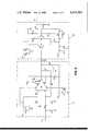
- FIG. 1is a diagram of apparatus for reducing the widths of pulses from a laser according to the invention.
- FIG. 2is an electrical schematic of some elements of the FIG. 1 apparatus.
- FIG. 3is an electrical schematic of some other elements of the FIG. 1 apparatus.
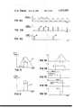
- FIG. 4Ais a graph of laser intensity (ordinate) versus time (abscissa) of a pulsed beam from a laser source.
- FIGS. 4B and 4Care graphs of laser intensity (ordinate) versus time (abscissa) for reduced-width pulses in an output beam according to the invention.
- FIG. 5is a graph of laser intensity (ordinate) versus time (abscissa) for a pulse from a laser source.
- FIG. 6is a graph of laser intensity (ordinate) versus time (abscissa) for the portion of the FIG. 5 pulse that is in the output beam of the FIG. 1 apparatus.
- FIGS. 7 A-Eare five graphs of voltage (ordinate) versus time (abscissa) appearing at different locations within the FIG. 1 circuitry.
- Electro optical crystal 20comprises two 6 cm ⁇ 6 cm ⁇ 30 cm crystals positioned serially lengthwise along the axis for travel of beam 12. Brass electrodes 24, 26 are on opposite lengthwise sides of crystal 20 on top of gold coatings (not shown). Leads 28, 30 connect electrodes 24, 26 to optical crystal driver circuitry 32. Electro optical crystal 20 and its electrodes have a 20 picofarad capacitance.
- Photodiode monitor 34is positioned on the opposite side of laser 14 from its output beam 12 to sense the leakage from the rear reflector of the laser. It provides a signal (peaking at approximately 1 volt) on line 35 to high speed comparator 36 (FIGS. 1 and 2), which senses the initial buildup of the signal from photodiode 34.
- Emitter follower 38(FIGS. 1 and 2) is connected between high speed comparator 36 and optical driver circuitry 32 to translate the comparator output to a 5 volt TTL signal on line 39.
- Variable delay circuit 40 and pulse width delay circuit 42are controlled by computer 44 and provide delayed signals on lines 45, 47 to field effect transistor (FET) drivers 46, 48, which are high speed, high current, low impedance drivers that convert the 5 volt input signal to a 30 volt output signal to drive the high voltage FET switches 50, 52, respectively.
- FETfield effect transistor
- Computer 44, pulse width delay circuit 42 and variable delay circuit 40are provided by a Teradyne M365 computer; alternatively, AM 685 components (available from Advanced Micro Circuits, Sunnyvale, Calif.) connected in the Schmidt trigger configuration can be used for circuits 40, 42.
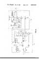
- FET driver 48 and high voltage FET switch 52are shown in detail.
- FET driver 46 and high voltage FET switch 50are identical to driver 48 and switch 52.
- Current drivers U2, U3are connected to drive FET's Q3, Q4 respectively.
- Transformer T(1:1 ratio; 3 turns #30 bifilar wire on a ferrite bead) is connected between U3 and Q4 to supply a signal to the gate of Q4 inverted from that supplied to the gate of Q3.
- Capacitor C29is connected to the 30 volt supply rail through diode D4 and to transistor Q4 to maintain the gate-source voltage of transistor Q4.
- High voltage FET's Q5, Q6, and Q7are connected in series.
- the gate of FET Q5is connected to FET's Q3, Q4, and the output of FET Q7 is connected through line 28 to crystal 20.
- the 40 and 50 volt supply railsare connected to drive the gates of FET's Q6, Q7, and the 450-700 volt supply rail is connected to the output of FET Q7.
- laser 14provides 200 nanosecond width pulses 55 at a repetition rate of up of 10 kHz. (This is shown in FIG. 4A; pulses 55 are in reality spaced from each other in time.)
- Laser beam 12which is polarized, is reflected by 100% reflector 16 so that it passes through polarizer 18 and lithium niobate crystal 20. After passing through crystal 20, beam 12 is reflected by 100% reflector 22, back through crystal 20 and then into polarizer 18. When no voltage appears across crystal 20, the pulses in beam 12 returning to polarizer 18 have the original polarization and pass straight through polarizer 18.
- the plane of polarizationWhen a voltage is applied to crystal 20, during the period that a portion of a pulse is passing through it, the plane of polarization will be rotated 90° (it is rotated by 45° on each passage through crystal 20), and the portion is deflected 90° at polarizer 18 to comprise output beam 54.
- the nominal wave shape of pulse 55 of beam 12is shown with dashed lines identifying the desired pulse width, ⁇ t.
- the delay time, Td, for beginning the desired output pulse after the beginning of pulse 55 of beam 12is also shown.
- the shape of the pulse in output 54is shown in FIG. 6. As is seen from FIGS.
- crystal 20can be activated to provide an output beam 45 with narrow (e.g., as short as ten nanoseconds) pulses 56, having the same repetition rate as the pulses in beam 12, or the repetition rate can be decreased by activating crystal 20 during selected pulses (e.g., 1 out of every 4 pulses) to obtain less-frequent narrow pulses 58.
- narrow pulses 56e.g., as short as ten nanoseconds
- the repetition ratecan be decreased by activating crystal 20 during selected pulses (e.g., 1 out of every 4 pulses) to obtain less-frequent narrow pulses 58.
- Photodiode monitor 34detects the leakage from the rear reflector of pulsed laser 14 and provides a signal (FIG. 7A) that has the same nominal wave shape as pulse 55 in laser beam 12 and peaks at approximately 1 volt.
- High-speed comparator 36senses the initial buildup of a signal from photodiode 34 and produces a trigger signal.
- variable delay circuit 40provides output signals similar to that shown in FIG. 7B; however, they are provided to FET driver 48 and pulse width delay circuit 42 at a time Td after the beginning of laser pulse 55.
- Pulse width delay circuit 42provides a signal which is similar to that shown in FIG. 7B to FET driver 46 and is delayed from the beginning of the pulse by an additional time period equal to the desired pulse width, ⁇ t.
- Computer 44controls variable delay circuit 40 and pulse width delay circuit 42.
- driver U2drives FET Q3 on, and driver U3 and transformer T drive FET Q4 off.
- FET Q3is turned on, a 30-volt, high current signal is provided to FET Q5 in high voltage switch 52, making FET Q5's gate-source voltage positive and turning it on, in turn making the gate-source voltages of FET's Q6 and Q7 positive, thereby causing the voltage on electrode 26 to drop from 450 volts to zero within a 5 nanosecond period, as is shown in FIG. 7C.
- the voltage at electrode 24is similarly decreased at a time ⁇ t later, as is shown in FIG. 7D.
- the effective voltage seen by crystal 20is presented in FIG. 7E.
- the voltage difference across the crystalgoes from zero up to 450 volts, at a time Td after the beginning of pulse 50, and returns to zero, at a time ⁇ t later.
- FET Q3While FET Q3 is on, capacitor C29 is charged by the 30 volt supply rail through diode D1.
- FET Q3When FET Q3 is turned off (at the end of the TTL signal), the gate voltage on FET Q4 goes to the 30 volts of the supply rail.
- the source of FET Q4begins to rise, the voltage across capacitor C29 is maintained, thereby maintaining the gate-source voltage of FET Q4 and turning off FET's Q5, Q6, and Q7.
- crystalscan be fabricated from potassium dihydrogen phosphate, deuterated potassium dihydrogen phosphate, or lithium tantalate.
Landscapes
- Physics & Mathematics (AREA)
- Nonlinear Science (AREA)
- Engineering & Computer Science (AREA)
- Optics & Photonics (AREA)
- Chemical & Material Sciences (AREA)
- Ceramic Engineering (AREA)
- Crystallography & Structural Chemistry (AREA)
- General Physics & Mathematics (AREA)
- Electromagnetism (AREA)
- Plasma & Fusion (AREA)
- Lasers (AREA)
Abstract
Description
Claims (13)
Priority Applications (1)
| Application Number | Priority Date | Filing Date | Title |
|---|---|---|---|
| US06/305,274US4483005A (en) | 1981-09-24 | 1981-09-24 | Affecting laser beam pulse width |
Applications Claiming Priority (1)
| Application Number | Priority Date | Filing Date | Title |
|---|---|---|---|
| US06/305,274US4483005A (en) | 1981-09-24 | 1981-09-24 | Affecting laser beam pulse width |
Publications (1)
| Publication Number | Publication Date |
|---|---|
| US4483005Atrue US4483005A (en) | 1984-11-13 |
Family
ID=23180141
Family Applications (1)
| Application Number | Title | Priority Date | Filing Date |
|---|---|---|---|
| US06/305,274Expired - Fee RelatedUS4483005A (en) | 1981-09-24 | 1981-09-24 | Affecting laser beam pulse width |
Country Status (1)
| Country | Link |
|---|---|
| US (1) | US4483005A (en) |
Cited By (23)
| Publication number | Priority date | Publication date | Assignee | Title |
|---|---|---|---|---|
| US4901323A (en)* | 1987-05-01 | 1990-02-13 | Universities Research Association, Inc. | Laser pulse stretcher method and apparatus |
| US5231536A (en)* | 1992-05-01 | 1993-07-27 | Xrl, Inc. | Robust, LED illumination system for OCR of indicia on a substrate |
| US5648976A (en)* | 1994-04-27 | 1997-07-15 | The United States Of America As Represented By The Secretary Of The Air Force | Laser with variable pulse length |
| US5737122A (en)* | 1992-05-01 | 1998-04-07 | Electro Scientific Industries, Inc. | Illumination system for OCR of indicia on a substrate |
| US5998759A (en)* | 1996-12-24 | 1999-12-07 | General Scanning, Inc. | Laser processing |
| US6141368A (en)* | 1998-05-13 | 2000-10-31 | The United States Of America As Represented By The Administrator Of The National Aeronautics And Space Administration | Method of controlling lasing wavelength(s) |
| US6281471B1 (en) | 1999-12-28 | 2001-08-28 | Gsi Lumonics, Inc. | Energy-efficient, laser-based method and system for processing target material |
| US6526089B1 (en) | 1999-09-29 | 2003-02-25 | Sunx Limited | Laser marker and method of light spot adjustment therefor |
| US20030189032A1 (en)* | 1998-12-16 | 2003-10-09 | General Scanning, A Massachusetts Corporation | Laser processing |
| US6703582B2 (en) | 1999-12-28 | 2004-03-09 | Gsi Lumonics Corporation | Energy-efficient method and system for processing target material using an amplified, wavelength-shifted pulse train |
| LT5168B (en) | 2003-01-22 | 2004-10-25 | Uždaroji akcinė bendrovė "EKSPLA" | Generator of short light pulses |
| US6831936B1 (en) | 1998-06-12 | 2004-12-14 | Gsi Lumonics Corporation | Pulse control in laser systems |
| US20050067388A1 (en)* | 2003-08-19 | 2005-03-31 | Yunlong Sun | Methods of and laser systems for link processing using laser pulses with specially tailored power profiles |
| US20060028655A1 (en)* | 2001-03-29 | 2006-02-09 | Gsil Lumonics Corporation | Methods and systems for precisely relatively positioning a waist of a pulsed laser beam and method and system for controlling energy delivered to a target structure |
| US20060045150A1 (en)* | 2004-09-02 | 2006-03-02 | Newman Leon A | Apparatus for modifying CO2 slab laser pulses |
| US20070233056A1 (en)* | 2006-02-08 | 2007-10-04 | The General Hospital Corporation | Methods, arrangements and systems for obtaining information associated with an anatomical sample using optical microscopy |
| US20080029491A1 (en)* | 2006-07-20 | 2008-02-07 | Gsi Group Corporation | System and method for laser processing at non-constant velocities |
| US7469831B2 (en) | 2004-06-30 | 2008-12-30 | Gsi Group Corporation | Laser-based method and system for processing targeted surface material and article produced thereby |
| US7482551B2 (en) | 2000-01-10 | 2009-01-27 | Electro Scientific Industries, Inc. | Processing a memory link with a set of at least two laser pulses |
| US7723642B2 (en) | 1999-12-28 | 2010-05-25 | Gsi Group Corporation | Laser-based system for memory link processing with picosecond lasers |
| US7838794B2 (en) | 1999-12-28 | 2010-11-23 | Gsi Group Corporation | Laser-based method and system for removing one or more target link structures |
| US8374206B2 (en) | 2008-03-31 | 2013-02-12 | Electro Scientific Industries, Inc. | Combining multiple laser beams to form high repetition rate, high average power polarized laser beam |
| US20130242380A1 (en)* | 2012-03-16 | 2013-09-19 | Kla-Tencor Corporation | Suppression Of Parasitic Optical Feedback In Pulse Laser Systems |
Citations (8)
| Publication number | Priority date | Publication date | Assignee | Title |
|---|---|---|---|---|
| US3564454A (en)* | 1967-11-28 | 1971-02-16 | Trw Inc | Laser apparatus with laser rod birefringence insensitive polarized cavity |
| US3673504A (en)* | 1967-11-28 | 1972-06-27 | Trw Inc | Laser with combined q-switch and synchronized cavity dump circuit |
| US3713032A (en)* | 1970-10-01 | 1973-01-23 | Westinghouse Electric Corp | Q-switching laser system having electronically controlled output coupling |
| US3737231A (en)* | 1970-11-13 | 1973-06-05 | G Low | High pulse rate high resolution optical radar system |
| US3780296A (en)* | 1972-12-22 | 1973-12-18 | Rca Ltd | Automatic optical bias control for light modulators |
| US3879686A (en)* | 1973-09-20 | 1975-04-22 | Us Air Force | Laser system for producing variable duration short pulses |
| US3898583A (en)* | 1972-03-29 | 1975-08-05 | Xerox Corp | Laser stabilization technique |
| US4243951A (en)* | 1978-06-12 | 1981-01-06 | Rca Corporation | High repetition rate driver circuit for modulation of injection lasers |
- 1981
- 1981-09-24USUS06/305,274patent/US4483005A/ennot_activeExpired - Fee Related
Patent Citations (8)
| Publication number | Priority date | Publication date | Assignee | Title |
|---|---|---|---|---|
| US3564454A (en)* | 1967-11-28 | 1971-02-16 | Trw Inc | Laser apparatus with laser rod birefringence insensitive polarized cavity |
| US3673504A (en)* | 1967-11-28 | 1972-06-27 | Trw Inc | Laser with combined q-switch and synchronized cavity dump circuit |
| US3713032A (en)* | 1970-10-01 | 1973-01-23 | Westinghouse Electric Corp | Q-switching laser system having electronically controlled output coupling |
| US3737231A (en)* | 1970-11-13 | 1973-06-05 | G Low | High pulse rate high resolution optical radar system |
| US3898583A (en)* | 1972-03-29 | 1975-08-05 | Xerox Corp | Laser stabilization technique |
| US3780296A (en)* | 1972-12-22 | 1973-12-18 | Rca Ltd | Automatic optical bias control for light modulators |
| US3879686A (en)* | 1973-09-20 | 1975-04-22 | Us Air Force | Laser system for producing variable duration short pulses |
| US4243951A (en)* | 1978-06-12 | 1981-01-06 | Rca Corporation | High repetition rate driver circuit for modulation of injection lasers |
Cited By (57)
| Publication number | Priority date | Publication date | Assignee | Title |
|---|---|---|---|---|
| US4901323A (en)* | 1987-05-01 | 1990-02-13 | Universities Research Association, Inc. | Laser pulse stretcher method and apparatus |
| US5231536A (en)* | 1992-05-01 | 1993-07-27 | Xrl, Inc. | Robust, LED illumination system for OCR of indicia on a substrate |
| US5737122A (en)* | 1992-05-01 | 1998-04-07 | Electro Scientific Industries, Inc. | Illumination system for OCR of indicia on a substrate |
| US5648976A (en)* | 1994-04-27 | 1997-07-15 | The United States Of America As Represented By The Secretary Of The Air Force | Laser with variable pulse length |
| US20020093997A1 (en)* | 1996-12-24 | 2002-07-18 | General Scanning, A Massachusetts Corporation | Laser processing |
| US6791059B2 (en) | 1996-12-24 | 2004-09-14 | Gsi Lumonics Corp. | Laser processing |
| US5998759A (en)* | 1996-12-24 | 1999-12-07 | General Scanning, Inc. | Laser processing |
| US6337462B1 (en) | 1996-12-24 | 2002-01-08 | General Scanning, Inc. | Laser processing |
| US20050173385A1 (en)* | 1996-12-24 | 2005-08-11 | Gsi Lumonics Corp., A Michiga Corporation | Laser processing |
| US6878899B2 (en) | 1996-12-24 | 2005-04-12 | Gsi Lumonics Corp. | Laser processing |
| US6141368A (en)* | 1998-05-13 | 2000-10-31 | The United States Of America As Represented By The Administrator Of The National Aeronautics And Space Administration | Method of controlling lasing wavelength(s) |
| US20050271095A1 (en)* | 1998-06-12 | 2005-12-08 | Smart Donald V | Pulse control in laser systems |
| US6831936B1 (en) | 1998-06-12 | 2004-12-14 | Gsi Lumonics Corporation | Pulse control in laser systems |
| US6973104B2 (en) | 1998-06-12 | 2005-12-06 | Gsi Lumonics Corporation | Pulse control in laser systems |
| EP1097492A4 (en)* | 1998-06-12 | 2005-05-11 | Gen Scanning Inc | PULSE CONTROL IN LASER SYSTEMS |
| US20030189032A1 (en)* | 1998-12-16 | 2003-10-09 | General Scanning, A Massachusetts Corporation | Laser processing |
| US20060283845A1 (en)* | 1998-12-16 | 2006-12-21 | William Lauer | Laser processing |
| US20050211682A1 (en)* | 1998-12-16 | 2005-09-29 | Gsi Lumonics Corp. | Laser processing |
| US6911622B2 (en) | 1998-12-16 | 2005-06-28 | General Scanning, Inc. | Laser processing |
| US6526089B1 (en) | 1999-09-29 | 2003-02-25 | Sunx Limited | Laser marker and method of light spot adjustment therefor |
| US6281471B1 (en) | 1999-12-28 | 2001-08-28 | Gsi Lumonics, Inc. | Energy-efficient, laser-based method and system for processing target material |
| US6703582B2 (en) | 1999-12-28 | 2004-03-09 | Gsi Lumonics Corporation | Energy-efficient method and system for processing target material using an amplified, wavelength-shifted pulse train |
| US8253066B2 (en) | 1999-12-28 | 2012-08-28 | Gsi Group Corporation | Laser-based method and system for removing one or more target link structures |
| US7838794B2 (en) | 1999-12-28 | 2010-11-23 | Gsi Group Corporation | Laser-based method and system for removing one or more target link structures |
| US7750268B2 (en) | 1999-12-28 | 2010-07-06 | Gsi Group Corporation | Energy efficient, laser-based method and system for processing target material |
| US6727458B2 (en) | 1999-12-28 | 2004-04-27 | Gsi Lumonics, Inc. | Energy-efficient, laser-based method and system for processing target material |
| US7723642B2 (en) | 1999-12-28 | 2010-05-25 | Gsi Group Corporation | Laser-based system for memory link processing with picosecond lasers |
| US7679030B2 (en) | 1999-12-28 | 2010-03-16 | Gsi Group Corporation | Energy-efficient, laser-based method and system for processing target material |
| US7582848B2 (en) | 1999-12-28 | 2009-09-01 | Gsi Group Corp | Energy-efficient, laser-based method and system for processing target material |
| US8338746B2 (en) | 2000-01-10 | 2012-12-25 | Electro Scientific Industries, Inc. | Method for processing a memory link with a set of at least two laser pulses |
| US7482551B2 (en) | 2000-01-10 | 2009-01-27 | Electro Scientific Industries, Inc. | Processing a memory link with a set of at least two laser pulses |
| US7671295B2 (en) | 2000-01-10 | 2010-03-02 | Electro Scientific Industries, Inc. | Processing a memory link with a set of at least two laser pulses |
| US7955905B2 (en) | 2001-03-29 | 2011-06-07 | Gsi Group Corporation | Methods and systems for thermal-based laser processing a multi-material device |
| US20060028655A1 (en)* | 2001-03-29 | 2006-02-09 | Gsil Lumonics Corporation | Methods and systems for precisely relatively positioning a waist of a pulsed laser beam and method and system for controlling energy delivered to a target structure |
| US7394476B2 (en) | 2001-03-29 | 2008-07-01 | Gsi Group Corporation | Methods and systems for thermal-based laser processing a multi-material device |
| US8217304B2 (en) | 2001-03-29 | 2012-07-10 | Gsi Group Corporation | Methods and systems for thermal-based laser processing a multi-material device |
| US7382389B2 (en) | 2001-03-29 | 2008-06-03 | Gsi Lumonics Corporation | Methods and systems for thermal-based laser processing a multi-material device |
| US8193468B2 (en) | 2001-03-29 | 2012-06-05 | Gsi Group Corporation | Methods and systems for precisely relatively positioning a waist of a pulsed laser beam and method and system for controlling energy delivered to a target structure |
| US8809734B2 (en) | 2001-03-29 | 2014-08-19 | Electron Scientific Industries, Inc. | Methods and systems for thermal-based laser processing a multi-material device |
| US7955906B2 (en) | 2001-03-29 | 2011-06-07 | Gsi Group Corporation | Methods and systems for thermal-based laser processing a multi-material device |
| LT5168B (en) | 2003-01-22 | 2004-10-25 | Uždaroji akcinė bendrovė "EKSPLA" | Generator of short light pulses |
| US20050067388A1 (en)* | 2003-08-19 | 2005-03-31 | Yunlong Sun | Methods of and laser systems for link processing using laser pulses with specially tailored power profiles |
| US7348516B2 (en) | 2003-08-19 | 2008-03-25 | Electro Scientific Industries, Inc. | Methods of and laser systems for link processing using laser pulses with specially tailored power profiles |
| US7469831B2 (en) | 2004-06-30 | 2008-12-30 | Gsi Group Corporation | Laser-based method and system for processing targeted surface material and article produced thereby |
| WO2006026143A3 (en)* | 2004-09-02 | 2006-07-13 | Coherent Inc | Apparatus for modifying co2 slab laser pulses |
| US20060045150A1 (en)* | 2004-09-02 | 2006-03-02 | Newman Leon A | Apparatus for modifying CO2 slab laser pulses |
| US7508850B2 (en) | 2004-09-02 | 2009-03-24 | Coherent, Inc. | Apparatus for modifying CO2 slab laser pulses |
| US20070233056A1 (en)* | 2006-02-08 | 2007-10-04 | The General Hospital Corporation | Methods, arrangements and systems for obtaining information associated with an anatomical sample using optical microscopy |
| US9777053B2 (en)* | 2006-02-08 | 2017-10-03 | The General Hospital Corporation | Methods, arrangements and systems for obtaining information associated with an anatomical sample using optical microscopy |
| US10351616B2 (en)* | 2006-02-08 | 2019-07-16 | The General Hospital Corporation | Methods, arrangements and systems for obtaining information associated with an anatomical sample using optical microscopy |
| US10800831B2 (en) | 2006-02-08 | 2020-10-13 | The General Hospital Corporation | Systems and methods for obtaining information associated with an anatomical sample using optical microscopy |
| US11319357B2 (en) | 2006-02-08 | 2022-05-03 | The General Hospital Corporation | Methods, arrangements and systems for obtaining information associated with an anatomical sample using optical microscopy |
| US8084706B2 (en) | 2006-07-20 | 2011-12-27 | Gsi Group Corporation | System and method for laser processing at non-constant velocities |
| US20080029491A1 (en)* | 2006-07-20 | 2008-02-07 | Gsi Group Corporation | System and method for laser processing at non-constant velocities |
| US8374206B2 (en) | 2008-03-31 | 2013-02-12 | Electro Scientific Industries, Inc. | Combining multiple laser beams to form high repetition rate, high average power polarized laser beam |
| US20130242380A1 (en)* | 2012-03-16 | 2013-09-19 | Kla-Tencor Corporation | Suppression Of Parasitic Optical Feedback In Pulse Laser Systems |
| US8767291B2 (en)* | 2012-03-16 | 2014-07-01 | Kla-Tencor Corporation | Suppression of parasitic optical feedback in pulse laser systems |
Similar Documents
| Publication | Publication Date | Title |
|---|---|---|
| US4483005A (en) | Affecting laser beam pulse width | |
| CN101983421B (en) | Methods and systems for dynamically generating tailored laser pulses | |
| US5548234A (en) | System and method for control of a Pockel's cell | |
| US7649667B2 (en) | Controlling pockels cells | |
| US11364078B2 (en) | Electro-optic Q-switching double-frequency double-pulse laser lithotripsy system | |
| US5394415A (en) | Method and apparatus for modulating optical energy using light activated semiconductor switches | |
| EP1418460B1 (en) | Driver citcuit for Pockels cell and laser system with such a driver circuit and a pockels cell | |
| US7508850B2 (en) | Apparatus for modifying CO2 slab laser pulses | |
| US20050224469A1 (en) | Efficient micro-machining apparatus and method employing multiple laser beams | |
| EP0281068B1 (en) | Laser marker and method of laser marking | |
| JP2008521611A (en) | High energy pulse suppression method | |
| US8536929B2 (en) | High voltage switch with adjustable current | |
| US4477905A (en) | Short pulse laser | |
| JP3055904B2 (en) | High voltage pulse generator | |
| US4629993A (en) | Pockels cell driver | |
| US6421390B1 (en) | High-speed pulse-shape generator, pulse multiplexer | |
| US4454430A (en) | Universal control grid modulator | |
| US4667161A (en) | Pulse shaping with transmission lines | |
| JPS63276037A (en) | Time modulation frequency multiplying laser light source | |
| US5594256A (en) | High voltage switch for pockels cells | |
| US5546011A (en) | Voltage measuring apparatus | |
| KR960025328A (en) | Magneto-optical recording apparatus using magnetic head driving circuit and magnetic head driving circuit operable with recording data transmitted by high speed transmission | |
| US3626326A (en) | Time-variable reflectivity laser actuating circuit | |
| JPS60119786A (en) | Q switch laser device | |
| JPH10247755A (en) | Laser light regeneration amplifier |
Legal Events
| Date | Code | Title | Description |
|---|---|---|---|
| AS | Assignment | Owner name:TERADYNE, INC., BOSTON, MA A CORP. OF MA Free format text:ASSIGNMENT OF ASSIGNORS INTEREST.;ASSIGNOR:SMART, DONALD V.;REEL/FRAME:003933/0533 Effective date:19810909 | |
| FEPP | Fee payment procedure | Free format text:PAYOR NUMBER ASSIGNED (ORIGINAL EVENT CODE: ASPN); ENTITY STATUS OF PATENT OWNER: LARGE ENTITY | |
| FPAY | Fee payment | Year of fee payment:4 | |
| AS | Assignment | Owner name:TERADYNE LASER SYSTEMS, INC., A MASSACHUSETTS CORP Free format text:ASSIGNMENT OF ASSIGNORS INTEREST.;ASSIGNOR:TERADYNE, INC.,;REEL/FRAME:005018/0907 Effective date:19890103 | |
| AS | Assignment | Owner name:TERADYNE LASER SYSTEMS, INC., A MA CORP., MASSACHU Free format text:ASSIGNMENT OF ASSIGNORS INTEREST.;ASSIGNOR:TERADYNE, INC.,;REEL/FRAME:005328/0384 Effective date:19900529 | |
| REMI | Maintenance fee reminder mailed | ||
| LAPS | Lapse for failure to pay maintenance fees | ||
| FP | Lapsed due to failure to pay maintenance fee | Effective date:19921115 | |
| STCH | Information on status: patent discontinuation | Free format text:PATENT EXPIRED DUE TO NONPAYMENT OF MAINTENANCE FEES UNDER 37 CFR 1.362 |