US4469976A - Single-side connected transducer - Google Patents
Single-side connected transducerDownload PDFInfo
- Publication number
- US4469976A US4469976AUS06/395,546US39554682AUS4469976AUS 4469976 AUS4469976 AUS 4469976AUS 39554682 AUS39554682 AUS 39554682AUS 4469976 AUS4469976 AUS 4469976A
- Authority
- US
- United States
- Prior art keywords
- transducer
- substrate
- interconnections
- electrical
- connections
- Prior art date
- Legal status (The legal status is an assumption and is not a legal conclusion. Google has not performed a legal analysis and makes no representation as to the accuracy of the status listed.)
- Expired - Lifetime
Links
Images
Classifications
- G—PHYSICS
- G10—MUSICAL INSTRUMENTS; ACOUSTICS
- G10K—SOUND-PRODUCING DEVICES; METHODS OR DEVICES FOR PROTECTING AGAINST, OR FOR DAMPING, NOISE OR OTHER ACOUSTIC WAVES IN GENERAL; ACOUSTICS NOT OTHERWISE PROVIDED FOR
- G10K11/00—Methods or devices for transmitting, conducting or directing sound in general; Methods or devices for protecting against, or for damping, noise or other acoustic waves in general
- G10K11/18—Methods or devices for transmitting, conducting or directing sound
- G10K11/26—Sound-focusing or directing, e.g. scanning
- G10K11/32—Sound-focusing or directing, e.g. scanning characterised by the shape of the source
- H—ELECTRICITY
- H10—SEMICONDUCTOR DEVICES; ELECTRIC SOLID-STATE DEVICES NOT OTHERWISE PROVIDED FOR
- H10N—ELECTRIC SOLID-STATE DEVICES NOT OTHERWISE PROVIDED FOR
- H10N15/00—Thermoelectric devices without a junction of dissimilar materials; Thermomagnetic devices, e.g. using the Nernst-Ettingshausen effect
- H10N15/10—Thermoelectric devices using thermal change of the dielectric constant, e.g. working above and below the Curie point
- H—ELECTRICITY
- H10—SEMICONDUCTOR DEVICES; ELECTRIC SOLID-STATE DEVICES NOT OTHERWISE PROVIDED FOR
- H10N—ELECTRIC SOLID-STATE DEVICES NOT OTHERWISE PROVIDED FOR
- H10N30/00—Piezoelectric or electrostrictive devices
- H10N30/80—Constructional details
- H10N30/87—Electrodes or interconnections, e.g. leads or terminals
- H10N30/875—Further connection or lead arrangements, e.g. flexible wiring boards, terminal pins
- Y—GENERAL TAGGING OF NEW TECHNOLOGICAL DEVELOPMENTS; GENERAL TAGGING OF CROSS-SECTIONAL TECHNOLOGIES SPANNING OVER SEVERAL SECTIONS OF THE IPC; TECHNICAL SUBJECTS COVERED BY FORMER USPC CROSS-REFERENCE ART COLLECTIONS [XRACs] AND DIGESTS
- Y10—TECHNICAL SUBJECTS COVERED BY FORMER USPC
- Y10S—TECHNICAL SUBJECTS COVERED BY FORMER USPC CROSS-REFERENCE ART COLLECTIONS [XRACs] AND DIGESTS
- Y10S310/00—Electrical generator or motor structure
- Y10S310/80—Piezoelectric polymers, e.g. PVDF
Definitions
- the present inventionrelates to the formation of transducers and more particularly to the formation of transducers utilizing heat-sensitive piezoelectric substrate.
- PVF 2Polyvinylidene fluoride
- non-destructive testing applicationssuch as acoustic emission and ultrasonic pulse echo testing, particularly from aircraft components under fatigue test.
- Such transducersare less brittle than ceramic piezoelectric transducers, and have other highly desirable properties.
- Colletti, A. L. Flexible PVF 2 FilmAn Exceptional Polymer for Transducers, in Science, 200 (4348): p. 1371-1374, June 23, 1978. Higher frequency transducers are needed to detect smaller critical flaws, but at frequencies of 20 MHz and above, ceramic piezoelectrics are thin and fragile, a problem not encountered with PVF 2 .
- PVF 2can function at higher power levels than many ceramic piezoelectric elements without suffering dielectric breakdown and subsequent failure.
- PVF 2 filmshave also been used as diaphragms for loudspeakers and earphones.
- One method that is utilized to make effective connections to PVF 2is to utilize an epoxy disposed between and attaching a conductor to a PVF 2 film and a contiguous electrical conductive coating applied to adjacent portions to electrically connect them as shown in U.S. Pat. No. 4,339,683.
- conductive coatings and wire leadsbe formed and attached on opposite sides of the film to form an active transducer area therebetween.
- Positioning the electrical connection on both sides of the substrateobstructs adhesive fastening to operational structures and prevents utilization of such transducers in structures which physically require that they be adhesively fastened with a smooth strong bond line.
- the production of operational structures utilizing transducers with electrical connections on both sidesare costly and time consuming since the connections must be made prior to mounting on the structure. Additionally, when the electrical connections are on both sides and one of such sides is attached to the structure it becomes increasingly difficult to prevent the leads from shorting to the structure.
- transducerhaving strong, durable electrical connections, which have good current carrying capacity, good mechanical strength, do not burn out with normally expected use, need not be applied to previous metallization, do not adversely affect the device to which it is applied, and which are capable of reliable transfer of electrical signals therethrough.
- Further objects of the present inventionare to provide a transducer having a strong, durable electrical connection with low contact resistance, reducing localized heating at high electrical loads of the material to which the lead is attached, reducing arcing and electrical anomalies of that type to prevent resultant localized damage to the connected members from heating, reducing damage to metalization caused by arcing, providing thermal protection to heat-sensitive substrates to which the connection is applied, and preventing breakdown of the connection.
- Still other objects of the present inventionare to provide a transducer having soldered connections to a heat-sensitive member or device without damaging that member or device.
- Still further objects of the present inventionare to provide a piezoelectric transducer which is flexible and lightweight, having lead attachment points or electrical connections which are disposed away from the acoustically active area of the transducer to keep the field of the active area of the transducer away from acoustical or electrical anomalies produced by the lead attachment point(s), reducing anomalies in beam pattern, preventing arcing between plates of the transducer, preventing localized arcing near the surface of the transducer, and preventing breakdown of or damage to the connection or to the transducer material.
- Another object of the present inventionis to provide a transducer having a heat-sensitive piezoelectric substrate with electrical interconnections positioned to minimize shorting out thereof to operational structure.
- a further object of the present inventionis to provide a transducer having a heat-sensitive piezoelectric substrate having electrical interconnections positioned thereon so that transducer manufacture is simplified for quantity production.
- Still another object of the present inventionis to provide a transducer having electrodes of various shapes and sizes to vary the power channeled into the respective electrode.
- a still further object of the present inventionis to provide a transducer having electrode patterns for providing focusing of signals radiated therefrom.
- the metalization on the underside of the substrateis vacuum deposited using a mask over the inappropriate regions.
- the interconnectionincludes adhesive material such as epoxy disposed between and attaching an electrically conductive member to one side of the heat sensitive piezoelectric substrate and a single contiguous electrically conductive coating applied to adjacent portions of these two members to electrically connect them.
- the substratecan first be partially masked to expose only those portions which are to receive the conductive coating.
- connectionone or more wires or electrodes, are fixed to the substrate with epoxy. Adjacent areas of the wires and of the substrate are then coated with a contiguous conductive coating such as by sputtering gold thereon.
- the substrateshould be masked before coating, and then unmasked after applying the coating, especially where multiple connections are desired, to prevent arcing or undesired interconnection between the coatings of the respective connections. Appropriate masking and positioning of the connections also keeps the field of the active area of the transducer away from electrical and acoustic anomalies produced by the connection(s).
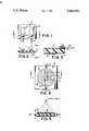
- FIG. 1is a plan view of a preferred embodiment of a piezoelectric transducer according to the present invention
- FIG. 2shows an end elevation view of the transducer of FIG. 1;
- FIG. 3shows a side elevation view of a transducer according to the present invention
- FIG. 4shows a plan view of another preferred embodiment of a concentric ring focusing transducer according to the invention.
- FIG. 5shows a side elevation of the transducer FIG. 4, showing a focal point resulting therefrom.
- FIGS. 1 and 2there is shown in FIGS. 1 and 2 a transducer 11 including a strip of film of polyvinylidene fluoride (PVF 2 ) or other appropriate material 13 provided with conductive coatings 15 and 17 formed on the same side of the film and which are configured to form two thin metallic parallel transducer plates.
- a metalized plate 18is vacuum deposited under coatings 15 and 17 and in a continuous perpendicular region therebetween. A mask is used to prevent metalization from depositing on inappropriate regions. Plates 15 and 17, and metalized plate 18 together define an active transducer area 19 immediately therebetween and bounded by the respective faces of plates 15 and 18 and 17 and 18.
- Film 13can for example be one inch long by 0.25 inch wide by 30 or 9 microns thick.
- Conductive coatings 15 and 17are respectively connected to wire leads 21 and 23 via respective connections 25 and 27.
- Coatings 15 and 17can for example each be of sputtered gold.
- Electrical signalscan be provided to active area 19 via coatings 15 and 17 from respective wires 21 and 23 connected thereto.
- a metallization-free borderis provided about the edge of film 13 to prevent arcing between coatings 15, 17 and plate 18 about the edges of transducer 11.
- active transducers area 19is displaced from the area of connections 25 and 27 to prevent electrical or acoustic anomalies about the connections from interfering with or appearing in the active area.
- connection 27includes a respective adhesive layer 31 such as of epoxy bonding respective wire 23 to film 13, and a respective metal or other conductive layer 17 such as of sputtered gold electrically connecting respective wire 23 to film 13.
- Connection 27can additionally be provided with an additional protective layer of adhesive 33 such as of epoxy to provide heat dissipation from, and ensure mechanical strength of the connection.
- Conductive layer 17also serves as the transducer 11 plate, so that there is direct electrical connection between the respective plate and respective lead wire 23.
- a transducer 40 including a strip of film (PVF 2 ) 39is provided with conductive coatings 45 and 47 formed on the same side of the film and which are configured to form thin metallic concentric transducer plates.
- Conductive coating 45extends over connection 43 and radially therefrom in opposite direction creating a first circumferential plate or electrode having a diameter d3 and extending toward the center thereof and again radially in opposite directions creating a second circumferential electrode having a smaller diameter d1.
- a small segment of the first and second electrode in alignment with connection 43is uncoated so that conductive coating 47 can extend over connection 44 and radially therefrom in opposite directions creating an interradial circumferential electrode having a diameter d2 and a center portion extending within said second electrode.
- conductive coating 47can extend over connection 44 and radially therefrom in opposite directions creating an interradial circumferential electrode having a diameter d2 and a center portion extending within said second electrode.
- the concentric platesform a Fresnel zone pattern thereby providing transducer focusing.
- Coatings 45 and 47form upper electrodes that may be constructed in various shapes and sizes to vary power channeled into either electrode.
- a metalized plate 49is vacuum deposited forming a lower electrode under coatings 45 and 47.
- the combination of upper electrodes and lower electrodescomprises an active transducer area 39 immediately therebetween and bounded by the respective faces of plates 45 and 49 and 57 and 49.
- Conductive coatings 45 and 47are respectively connected to wire leads 41 and 42 via respective connections 43 and 44.
- Coatings 45 and 47can for example, each be of sputtered gold.
- Electrical signalscan be provided to the active transducer area via coatings 45 and 47 from respective wires 41 and 42 connected thereto.
- Active transducer areais displaced from the area of connections 43 and 44 to prevent electrical or acoustic anomalies about the connections from interfering with or appearing in the active area.
- Connections 43 and 44are similar to connections 25 and 27.
- substratessuch as PVF 2 films can be provided with reliable electrical connections on one side thereof and to form a reliable transducer according to the present invention.
- any desired number of connections and transducerscan be provided to such a substrate if appropriate masking is used.
- the connectionsneed not be placed on opposite sides of the film 13 or 39 but can, for example, be disposed on the same side of film 13 or 39 in different configurations or patterns on the plane of the film, with the active area of the transducer between the faces of the conductive coating and displaced from the connections to avoid anomalies.
- a novel transducerhaving strong, reliable mechanical and electrical interconnection between a wire and one side of a heat sensitive piezoelectric substrate.
- a transduceris thereby provided with lead attachment points on one side of a heat sensitive piezoelectric substrate relatively remote from the active area, preventing high fields (e.g. 0.2 ⁇ 10 6 volts/cm.) from building up near lead attachment points. Such fields can produce arcing and subsequent burnout near the lead attachment points. Displacing the active area from the electrical connections also maintains the field of the active area away from electrical or acoustic anomalies produced by the lead attachment point.
- a transduceris provided having a heat-sensitive piezoelectric substrate with electrical interconnections positioned for minimizing lead short out to operational structure, for manufacturing simplification.
- a transducerhaving various electrode shapes, sizes and patterns to vary the power channeled therein and effecting transducer focusing.
Landscapes
- Physics & Mathematics (AREA)
- Engineering & Computer Science (AREA)
- Acoustics & Sound (AREA)
- Multimedia (AREA)
- Transducers For Ultrasonic Waves (AREA)
Abstract
Description
Claims (1)
Priority Applications (1)
| Application Number | Priority Date | Filing Date | Title |
|---|---|---|---|
| US06/395,546US4469976A (en) | 1982-07-06 | 1982-07-06 | Single-side connected transducer |
Applications Claiming Priority (1)
| Application Number | Priority Date | Filing Date | Title |
|---|---|---|---|
| US06/395,546US4469976A (en) | 1982-07-06 | 1982-07-06 | Single-side connected transducer |
Publications (1)
| Publication Number | Publication Date |
|---|---|
| US4469976Atrue US4469976A (en) | 1984-09-04 |
Family
ID=23563502
Family Applications (1)
| Application Number | Title | Priority Date | Filing Date |
|---|---|---|---|
| US06/395,546Expired - LifetimeUS4469976A (en) | 1982-07-06 | 1982-07-06 | Single-side connected transducer |
Country Status (1)
| Country | Link |
|---|---|
| US (1) | US4469976A (en) |
Cited By (21)
| Publication number | Priority date | Publication date | Assignee | Title |
|---|---|---|---|---|
| US4565942A (en)* | 1983-07-01 | 1986-01-21 | Murata Manufacturing Co., Ltd. | Energy trapped piezoelectric resonator liquid sensor |
| US4581556A (en)* | 1983-08-30 | 1986-04-08 | Murata Manufacturing Co., Ltd. | Double thickness mode energy trapped piezoelectric resonating device |
| US4780639A (en)* | 1986-05-22 | 1988-10-25 | Nec Corporation | Electrostriction effect element |
| EP0284055A3 (en)* | 1987-03-26 | 1989-01-25 | Washington Res Found | Endoscopically deliverable ultrasound imaging system |
| US4833659A (en)* | 1984-12-27 | 1989-05-23 | Westinghouse Electric Corp. | Sonar apparatus |
| EP0338711A3 (en)* | 1988-04-13 | 1991-06-26 | Kureha Kagaku Kogyo Kabushiki Kaisha | A pyroelectric element |
| US5030874A (en)* | 1985-05-20 | 1991-07-09 | Matsushita Electric Industrial Co., Ltd. | Ultrasonic probe |
| US5255016A (en)* | 1989-09-05 | 1993-10-19 | Seiko Epson Corporation | Ink jet printer recording head |
| US5716038A (en)* | 1992-08-13 | 1998-02-10 | Aztec Developments Limited | Proportional flow control valve |
| US5789846A (en)* | 1995-12-13 | 1998-08-04 | The Whitaker Corporation | Capacitively coupled ground electrode for piezo-electric film |
| US6051912A (en)* | 1997-02-24 | 2000-04-18 | Nikon Corporation | Vibration actuator |
| US6111342A (en)* | 1993-03-17 | 2000-08-29 | Seiko Instruments Inc. | Instrument for chemical measurement |
| US6323584B1 (en)* | 1995-09-06 | 2001-11-27 | Measurement Specialties Inc. | Interchangeable vessel having a level sensor therewith |
| US20050082951A1 (en)* | 2003-08-01 | 2005-04-21 | Pasi Tikka | Electrical component having overlapping electrodes, and method for the manufacture of same |
| US20060104774A1 (en)* | 2002-12-18 | 2006-05-18 | Sessler Laverne M Jr | Mobile receptacle for a catching debris |
| US20100263181A1 (en)* | 2001-05-22 | 2010-10-21 | Sri International | Rolled electroactive polymers |
| CN103706551A (en)* | 2013-12-19 | 2014-04-09 | 中国科学院苏州生物医学工程技术研究所 | Self-focusing type ultrasonic transducer based on Fresnel waveband type piezoelectric composite material |
| US20140218136A1 (en)* | 2011-11-01 | 2014-08-07 | Panasonic Corporation | Resonance coupler |
| US20150214597A1 (en)* | 2014-01-29 | 2015-07-30 | Panasonic Intellectual Property Management Co., Ltd. | Resonance coupler, transmission apparatus, switching system, and directional coupler |
| US9922638B2 (en)* | 2014-10-29 | 2018-03-20 | The United States Of America, As Represented By The Secretary Of The Navy | Acoustic fresnel zone plate lens for aqueous environments and methods of using same |
| US11100305B2 (en) | 2017-12-21 | 2021-08-24 | Fingerprint Cards Ab | Display arrangement comprising ultrasonic biometric sensing system and method for manufacturing the display arrangement |
Citations (10)
| Publication number | Priority date | Publication date | Assignee | Title |
|---|---|---|---|---|
| US2875355A (en)* | 1954-05-24 | 1959-02-24 | Gulton Ind Inc | Ultrasonic zone plate focusing transducer |
| US3940637A (en)* | 1973-10-15 | 1976-02-24 | Toray Industries, Inc. | Polymeric piezoelectric key actuated device |
| US3971250A (en)* | 1975-02-18 | 1976-07-27 | Minnesota Mining And Manufacturing Company | Electret sensing medium having plural sensing units |
| US4071785A (en)* | 1975-05-02 | 1978-01-31 | Kureha Kagaku Kogyo Kabushiki Kaisha | Laminated piezoelectric matrix switch |
| US4184095A (en)* | 1977-04-08 | 1980-01-15 | Telettra Laboratori de Telafonia Elettronica E Radio S.p.A. | Quartz crystal resonator with supplemental electrodes for controlling the Q factor |
| US4218631A (en)* | 1977-06-08 | 1980-08-19 | Kinsekisha Laboratory, Ltd. | Electrode structure for thickness mode piezoelectric vibrating elements |
| US4325060A (en)* | 1979-12-17 | 1982-04-13 | Purtell Jack L | Floating water detector |
| US4339683A (en)* | 1980-02-04 | 1982-07-13 | The United States Of America As Represented By The Secretary Of The Navy | Electrical connection |
| US4356421A (en)* | 1980-03-25 | 1982-10-26 | Tohoku Metal Industries, Ltd. | Piezoelectric resonators of an energy-trapping type of a width extensional vibratory mode |
| JPS58391A (en)* | 1981-06-25 | 1983-01-05 | Sumitomo Metal Ind Ltd | Submerged welding method for high temperature steel |
- 1982
- 1982-07-06USUS06/395,546patent/US4469976A/ennot_activeExpired - Lifetime
Patent Citations (10)
| Publication number | Priority date | Publication date | Assignee | Title |
|---|---|---|---|---|
| US2875355A (en)* | 1954-05-24 | 1959-02-24 | Gulton Ind Inc | Ultrasonic zone plate focusing transducer |
| US3940637A (en)* | 1973-10-15 | 1976-02-24 | Toray Industries, Inc. | Polymeric piezoelectric key actuated device |
| US3971250A (en)* | 1975-02-18 | 1976-07-27 | Minnesota Mining And Manufacturing Company | Electret sensing medium having plural sensing units |
| US4071785A (en)* | 1975-05-02 | 1978-01-31 | Kureha Kagaku Kogyo Kabushiki Kaisha | Laminated piezoelectric matrix switch |
| US4184095A (en)* | 1977-04-08 | 1980-01-15 | Telettra Laboratori de Telafonia Elettronica E Radio S.p.A. | Quartz crystal resonator with supplemental electrodes for controlling the Q factor |
| US4218631A (en)* | 1977-06-08 | 1980-08-19 | Kinsekisha Laboratory, Ltd. | Electrode structure for thickness mode piezoelectric vibrating elements |
| US4325060A (en)* | 1979-12-17 | 1982-04-13 | Purtell Jack L | Floating water detector |
| US4339683A (en)* | 1980-02-04 | 1982-07-13 | The United States Of America As Represented By The Secretary Of The Navy | Electrical connection |
| US4356421A (en)* | 1980-03-25 | 1982-10-26 | Tohoku Metal Industries, Ltd. | Piezoelectric resonators of an energy-trapping type of a width extensional vibratory mode |
| JPS58391A (en)* | 1981-06-25 | 1983-01-05 | Sumitomo Metal Ind Ltd | Submerged welding method for high temperature steel |
Non-Patent Citations (2)
| Title |
|---|
| PVF 2 Transducers, by Shaw et al, Proceedings of IEEE Ultrasonics Symposium, Boston, Ma., Nov. 5 7, 1980.* |
| PVF2 Transducers, by Shaw et al, Proceedings of IEEE Ultrasonics Symium, Boston, Ma., Nov. 5-7, 1980. |
Cited By (26)
| Publication number | Priority date | Publication date | Assignee | Title |
|---|---|---|---|---|
| US4565942A (en)* | 1983-07-01 | 1986-01-21 | Murata Manufacturing Co., Ltd. | Energy trapped piezoelectric resonator liquid sensor |
| US4581556A (en)* | 1983-08-30 | 1986-04-08 | Murata Manufacturing Co., Ltd. | Double thickness mode energy trapped piezoelectric resonating device |
| US4833659A (en)* | 1984-12-27 | 1989-05-23 | Westinghouse Electric Corp. | Sonar apparatus |
| US5030874A (en)* | 1985-05-20 | 1991-07-09 | Matsushita Electric Industrial Co., Ltd. | Ultrasonic probe |
| US4780639A (en)* | 1986-05-22 | 1988-10-25 | Nec Corporation | Electrostriction effect element |
| EP0284055A3 (en)* | 1987-03-26 | 1989-01-25 | Washington Res Found | Endoscopically deliverable ultrasound imaging system |
| EP0338711A3 (en)* | 1988-04-13 | 1991-06-26 | Kureha Kagaku Kogyo Kabushiki Kaisha | A pyroelectric element |
| US5255016A (en)* | 1989-09-05 | 1993-10-19 | Seiko Epson Corporation | Ink jet printer recording head |
| US5841027A (en)* | 1992-08-13 | 1998-11-24 | Aztec Development Ltd | Piezoelectric flow transducer |
| US5716038A (en)* | 1992-08-13 | 1998-02-10 | Aztec Developments Limited | Proportional flow control valve |
| US6111342A (en)* | 1993-03-17 | 2000-08-29 | Seiko Instruments Inc. | Instrument for chemical measurement |
| US6323584B1 (en)* | 1995-09-06 | 2001-11-27 | Measurement Specialties Inc. | Interchangeable vessel having a level sensor therewith |
| US5789846A (en)* | 1995-12-13 | 1998-08-04 | The Whitaker Corporation | Capacitively coupled ground electrode for piezo-electric film |
| US6051912A (en)* | 1997-02-24 | 2000-04-18 | Nikon Corporation | Vibration actuator |
| US20100263181A1 (en)* | 2001-05-22 | 2010-10-21 | Sri International | Rolled electroactive polymers |
| US20060104774A1 (en)* | 2002-12-18 | 2006-05-18 | Sessler Laverne M Jr | Mobile receptacle for a catching debris |
| US20050082951A1 (en)* | 2003-08-01 | 2005-04-21 | Pasi Tikka | Electrical component having overlapping electrodes, and method for the manufacture of same |
| US7187109B2 (en)* | 2003-08-01 | 2007-03-06 | Epcos Ag | Electrical component having overlapping electrodes, and method for the manufacture of same |
| US20140218136A1 (en)* | 2011-11-01 | 2014-08-07 | Panasonic Corporation | Resonance coupler |
| US9391353B2 (en)* | 2011-11-01 | 2016-07-12 | Panasonic Intellectual Property Management Co., Ltd. | Resonance coupler |
| CN103706551A (en)* | 2013-12-19 | 2014-04-09 | 中国科学院苏州生物医学工程技术研究所 | Self-focusing type ultrasonic transducer based on Fresnel waveband type piezoelectric composite material |
| CN103706551B (en)* | 2013-12-19 | 2016-07-06 | 中国科学院苏州生物医学工程技术研究所 | Self-focusing type ultrasonic transducer based on Fresnel formula piezo-electricity composite material |
| US20150214597A1 (en)* | 2014-01-29 | 2015-07-30 | Panasonic Intellectual Property Management Co., Ltd. | Resonance coupler, transmission apparatus, switching system, and directional coupler |
| US9479074B2 (en)* | 2014-01-29 | 2016-10-25 | Panasonic Intellectual Property Management Co., Ltd. | Resonance coupler, transmission apparatus, switching system, and directional coupler |
| US9922638B2 (en)* | 2014-10-29 | 2018-03-20 | The United States Of America, As Represented By The Secretary Of The Navy | Acoustic fresnel zone plate lens for aqueous environments and methods of using same |
| US11100305B2 (en) | 2017-12-21 | 2021-08-24 | Fingerprint Cards Ab | Display arrangement comprising ultrasonic biometric sensing system and method for manufacturing the display arrangement |
Similar Documents
| Publication | Publication Date | Title |
|---|---|---|
| US4469976A (en) | Single-side connected transducer | |
| US4406059A (en) | Method for making a piezoelectric transducer | |
| US6996883B2 (en) | Method of manufacturing a multi-piezoelectric layer ultrasonic transducer for medical imaging | |
| US4078160A (en) | Piezoelectric bimorph or monomorph bender structure | |
| US5296651A (en) | Flexible circuit with ground plane | |
| US5091893A (en) | Ultrasonic array with a high density of electrical connections | |
| US6430109B1 (en) | Array of capacitive micromachined ultrasonic transducer elements with through wafer via connections | |
| US5655276A (en) | Method of manufacturing two-dimensional array ultrasonic transducers | |
| EP0210723B1 (en) | Ultrasonic probe | |
| US5600530A (en) | Electrostatic chuck | |
| US4395652A (en) | Ultrasonic transducer element | |
| US12269063B2 (en) | Ultrasound array transducer manufacturing | |
| US20010011857A1 (en) | Surface acoustic wave device and method for fabricating the same | |
| US4709361A (en) | Flexural disk transducer | |
| US4611372A (en) | Method for manufacturing an ultrasonic transducer | |
| US3453711A (en) | Method of connecting together a plurality of transducer segments | |
| JPS639376B2 (en) | ||
| EP0152189A2 (en) | Bonding electrical conductors and bonded products | |
| US4503350A (en) | Piezoelectric resonator device with a laminated structure | |
| KR20000069886A (en) | Method for making a sonoprobe | |
| US4546283A (en) | Conductor structure for thick film electrical device | |
| Scott et al. | Durable lead attachment techniques for pvdf polymer transducers with application to high voltage pulsed ultrasonics1 | |
| KR101145231B1 (en) | Piezoelectric sound producing unit | |
| JPH08307995A (en) | Ultrasonic probe | |
| JPH0833097A (en) | Piezoelectric element |
Legal Events
| Date | Code | Title | Description |
|---|---|---|---|
| AS | Assignment | Owner name:UNITED STATES REPRESENTED BY THE SECRETARY OF THE Free format text:ASSIGNMENT OF ASSIGNORS INTEREST.;ASSIGNOR:SCOTT, WILLIAM;REEL/FRAME:004052/0813 Effective date:19820702 Owner name:UNITED STATES REPRESENTED BY THE SECRETARY OF THE Free format text:ASSIGNMENT OF ASSIGNORS INTEREST;ASSIGNOR:SCOTT, WILLIAM;REEL/FRAME:004052/0813 Effective date:19820702 | |
| FPAY | Fee payment | Year of fee payment:4 | |
| FEPP | Fee payment procedure | Free format text:PETITION RELATED TO MAINTENANCE FEES FILED (ORIGINAL EVENT CODE: PMFP); ENTITY STATUS OF PATENT OWNER: LARGE ENTITY | |
| FEPP | Fee payment procedure | Free format text:PETITION RELATED TO MAINTENANCE FEES DENIED/DISMISSED (ORIGINAL EVENT CODE: PMFD); ENTITY STATUS OF PATENT OWNER: LARGE ENTITY | |
| REMI | Maintenance fee reminder mailed | ||
| FP | Lapsed due to failure to pay maintenance fee | Effective date:19920906 | |
| FEPP | Fee payment procedure | Free format text:PETITION RELATED TO MAINTENANCE FEES FILED (ORIGINAL EVENT CODE: PMFP); ENTITY STATUS OF PATENT OWNER: LARGE ENTITY | |
| FEPP | Fee payment procedure | Free format text:PETITION RELATED TO MAINTENANCE FEES GRANTED (ORIGINAL EVENT CODE: PMFG); ENTITY STATUS OF PATENT OWNER: LARGE ENTITY | |
| FPAY | Fee payment | Year of fee payment:8 | |
| SULP | Surcharge for late payment | ||
| STCF | Information on status: patent grant | Free format text:PATENTED CASE | |
| DP | Notification of acceptance of delayed payment of maintenance fee |