US4467422A - Array processor - Google Patents
Array processorDownload PDFInfo
- Publication number
- US4467422A US4467422AUS06/508,175US50817583AUS4467422AUS 4467422 AUS4467422 AUS 4467422AUS 50817583 AUS50817583 AUS 50817583AUS 4467422 AUS4467422 AUS 4467422A
- Authority
- US
- United States
- Prior art keywords
- data
- processing elements
- elements
- data processing
- code
- Prior art date
- Legal status (The legal status is an assumption and is not a legal conclusion. Google has not performed a legal analysis and makes no representation as to the accuracy of the status listed.)
- Expired - Lifetime
Links
Images


Classifications
- G—PHYSICS
- G11—INFORMATION STORAGE
- G11C—STATIC STORES
- G11C29/00—Checking stores for correct operation ; Subsequent repair; Testing stores during standby or offline operation
- G11C29/006—Checking stores for correct operation ; Subsequent repair; Testing stores during standby or offline operation at wafer scale level, i.e. wafer scale integration [WSI]
- G—PHYSICS
- G06—COMPUTING OR CALCULATING; COUNTING
- G06F—ELECTRIC DIGITAL DATA PROCESSING
- G06F11/00—Error detection; Error correction; Monitoring
- G06F11/07—Responding to the occurrence of a fault, e.g. fault tolerance
- G06F11/08—Error detection or correction by redundancy in data representation, e.g. by using checking codes
- G06F11/10—Adding special bits or symbols to the coded information, e.g. parity check, casting out 9's or 11's
- G—PHYSICS
- G06—COMPUTING OR CALCULATING; COUNTING
- G06F—ELECTRIC DIGITAL DATA PROCESSING
- G06F15/00—Digital computers in general; Data processing equipment in general
- G06F15/76—Architectures of general purpose stored program computers
- G06F15/80—Architectures of general purpose stored program computers comprising an array of processing units with common control, e.g. single instruction multiple data processors
- G06F15/8007—Architectures of general purpose stored program computers comprising an array of processing units with common control, e.g. single instruction multiple data processors single instruction multiple data [SIMD] multiprocessors
- G06F15/8023—Two dimensional arrays, e.g. mesh, torus
Definitions
- This inventionrelates to data processing systems of the kind comprising a plurality of processing elements logically arranged in rows and columns so that each element has four nearest neighboring elements.
- data processing systemsof the kind comprising a plurality of processing elements logically arranged in rows and columns so that each element has four nearest neighboring elements.
- Such a systemis described for example in British Patent Specification Nos. 1445714, 1536933, U.S. Pat. Nos. 4,270,170, 4,241,413, and 4,304,002.
- each elementit is usually desired to allow each element to send information to, and receive information from, any of its four nearest neighbors. In the specifications referred to above, this is achieved by connecting each element to its four neighbors by means of a separate connection path.
- One object of the present inventionis to reduce the number of connection paths required to transfer information between neighboring elements.
- a data processing systemcomprising a plurality of processing elements logically arranged in rows and columns, characterised in that each column is divided into a plurality of groups of elements, the elements within each group being connected together to permit information to be transferred northwards and southwards between adjacent elements within the same group, and characterized by a plurality of switching circuits each having two states, wherein
- the switching circuitsconnect the northernmost element of each group to the southernmost element of the adjacent group in the northern direction, thereby permitting information to be transferred northwards and southwards between adjacent groups in the same column, and
- the switching circuitsconnect the northernmost element of each group to the southernmost element of the adjacent group in the western direction, thereby permitting information to be transferred eastwards and westwards between adjacent groups in different columns.
- the inventionreplaces a plurality of east-west connections between members of an adjacent pair of groups by a single "diagonal" connection between the northermost element of one group and the southernmost element of the group to the west of it. Shifting of information eastwards or westwards is achieved by placing the switching circuits in their second states, and then performing a sequence of northward or southward shifts over the diagonal connections. It can be seen that the invention significantly reduces the number of connection paths.
- the systemcomprises a plurality of data processing elements and a plurality of check code processing elements, each check code processing element holding a check code (e.g. parity bits) in respect of a predetermined plurality of data processing elements.
- a check codee.g. parity bits
- the inventionis used to reduce the number of connections between the check code processing elements.
- the data processing elementsare connected in the conventional manner i.e. each having a separate connection path to each of its four neighbors.
- FIG. 1is an overall block diagram of the system
- FIG. 2shows the connections between the data processing elements, parity processing elements, and parity checking circuits
- FIG. 3shows the interconnections between the data processing elements
- FIG. 4shows a circuit in one of the data processing elements for selecting data inputs from neighboring elements
- FIG. 5shows the interconnections between the parity processing elements
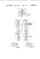
- FIGS. 6 and 7show two possible states of a switching circuit
- FIG. 8shows a circuit in one of the parity processing elements for selecting parity bit inputs from neighboring elements
- FIGS. 9 and 10illustrate possible ways of connecting parity processing elements consisting of LSI (large scale integrated circuit) chips.
- FIG. 1shows a data processing system comprising 4096 identical data processing elements D arranged in 64 rows and 64 columns.
- Each elementmay be of the form shown in the published patent specifications referred to above, and will therefore not be described in detail herein. Briefly, however, each element D contains a data store having a large number of individually addressable bit locations, various single-bit internal registers, a single-bit binary adder, and various gates for controlling the movement of data between the store, registers and adder.
- the elements Dare controlled by signals which are broadcast to all the elements in parallel, so that all the elements perform basically the same operations, but on different data.
- the array of elements Dis shown as being subdivided into sixty-four square sub-arrays 10, each containing 8 ⁇ 8 elements.
- Each sub-arrayhas a group 12 of eight parity processing elements P associated with it, one for each row.
- the parity processing elements Pare substantially identical with the data processing elements D, and are controlled by the same control signals, so that each parity processing element performs basically the same manipulations on the parity bits as the data processing elements perform on the data. For example, if a data bit is transferred from the store of each data processing element to one of its internal registers, the corresponding parity bit is transferred from the store of each parity processing element to the corresponding internal register in that element.
- FIG. 2shows one of the rows of data processing elements in a sub-array, and the corresponding parity processing element.
- Output data bits from the eight data processing elementsare fed to a parity checking circuit 14, where they are checked against the corresponding parity bit from the parity processing element. If there is an error, the checking circuit 14 generates an error signal. Parity checking is well known, and so it is not necessary to describe the circuit 14 in detail.
- FIG. 3shows the way in which the data processing elements are connected together to permit transfer of data between them.
- Each data processing element Dis connected to its four nearest neighbors in the north, east, south and west directions. The exception to this is at the boundaries of the array where, of course, the elements have fewer than four neighbors. However, the elements along the north edge of the array may be connected to those on the south edge so that each column consists effectively of a loop of elements. Similarly, the rows may be connected as loops.
- routing codewhich is broadcast from a controller to all the elements in parallel.
- the routing codeconsists of two bits, the significance of which is as follows:
- each data processing elementcontains a multiplexer 16 having four inputs 0, 1, 2, 3 connected to receive data from the four neighboring elements in the south, west, north and east directions respectively and an output 17.
- the multiplexer 16is controlled by the routing code on lines 19, so that it selects one of its four inputs in accordance with the binary value of the code. For example, if the routing code is 00, input 0 is selected, so that each element accepts data from its southern neighbor. As a result, data flows northwards.
- FIG. 5shows the way in which the parity processing elements P are interconnected. Within each group 12 they are interconnected by north-south connections 18. However, there are no east-west connections. Instead, transfer of parity bits between adjacent groups of parity processing elements in the east-west direction is achieved by diagonal paths 20 which connect the northernmost element in each group with the southernmost element in the adjacent group to the west. Switching circuits 22 are provided to determine whether the parity bits are to be shifted between adjacent groups in the north-south direction or over the diagonal paths 20.
- Each switching circuit 22has two states and is controlled by the second bit of the routing code.
- the switching circuitmakes the connection shown in FIG. 7 i.e. it connects the northernmost and southernmost elements to the respective diagonal paths 20.
- switching circuits 22are represented symbolically in the drawings as mechanical switches, in practice they are electronic switches constructed in a conventional manner from known logic components.
- each parity processing element Pcontains a multiplexer 40 having four inputs 0,1,2,3 and controlled by the routing code on lines 41 in a similar manner to the multiplexer 16 in FIG. 4. However, in this case, there is no connection from eastern and western neighbors. Instead, the input from the southern neighbor is connected to inputs 0 and 3, and the input from the northern neighbor is connected to inputs 1 and 2.
- the parity bitsare shifted nothwards within the groups of elements and are shifted over the diagonal paths 20 (because of the switching circuit connections shown in FIG. 7) between groups. It can be seen that after eight such shifts have been performed the contents of each group of parity processing elements willhave been shifted westwards into the adjacent group of parity processing elements, corresponding to the westward shift of data from one of the sub-arrays 10 (FIG. 1) into the adjacent sub-array.
- the parity bitsare shifted southwards within the groups and over the diagonal paths 20 between groups, so that after eight such shifts the contents of each group of parity processing elements will have been shifted eastwards into the adjacent group of parity processing elements.
- the data processing elements and parity processing elementsare preferably implemented in the form of LSI (large-scale integrated circuit) chips. Conveniently, four processing elements may be incorporated in each LSI chip, providing a 2 ⁇ 2 portion of the array. However, it can be seen from FIG. 5 that the parity processing elements must be connected in a linear manner rather than in a 2-dimensional array.
- LSIlarge-scale integrated circuit
- FIG. 9shows two LSI chips 40 and 42, each containing a 2 ⁇ 2 configuration of parity processing elements.
- the south-western element on each chiphas its southern connection 44 wired to the northern connection 46 of the north-eastern element on the same chip.
- the southern connection 48 from the south-eastern element on the upper chip 40is wired to the northern connection 50 from the north-western element on the lower chip 42.
- the effectis to join the eight elements in series, by way of their north-south connections, thus forming one of the groups 12 of parity processing elements shown in FIG. 5.
- FIG. 10shows the way in which two of these chips 52 and 54 would be connected to achieve the same effect as in FIG. 9.
- the arraycould be divided into rectangular sub-arrays instead of square sub-arrays.
- the number of steps needed to shift the parity bits in the east-west direction between adjacent groups, over the diagonal pathswould be different from the number of steps needed to shift the data bits between adjacent sub-arrays. It would therefore be necessary to introduce additional control circuits to inhibit some of the clock pulses to (or generate some extra clock pulses for) the parity processing elements during the east-west shifts to ensure that the parity bits were kept in the correct relationship to the data.
Landscapes
- Engineering & Computer Science (AREA)
- Theoretical Computer Science (AREA)
- Physics & Mathematics (AREA)
- General Engineering & Computer Science (AREA)
- General Physics & Mathematics (AREA)
- Computer Hardware Design (AREA)
- Quality & Reliability (AREA)
- Computing Systems (AREA)
- Error Detection And Correction (AREA)
- Multi Processors (AREA)
Abstract
Description
______________________________________ Routing code Direction ______________________________________ 00 North 01 East 10 South 11 West ______________________________________
Claims (5)
Applications Claiming Priority (2)
| Application Number | Priority Date | Filing Date | Title |
|---|---|---|---|
| GB8010574 | 1980-03-28 | ||
| GB8010574 | 1980-03-28 |
Related Parent Applications (1)
| Application Number | Title | Priority Date | Filing Date |
|---|---|---|---|
| US06240896Continuation | 1981-03-15 |
Publications (1)
| Publication Number | Publication Date |
|---|---|
| US4467422Atrue US4467422A (en) | 1984-08-21 |
Family
ID=10512474
Family Applications (1)
| Application Number | Title | Priority Date | Filing Date |
|---|---|---|---|
| US06/508,175Expired - LifetimeUS4467422A (en) | 1980-03-28 | 1983-06-27 | Array processor |
Country Status (5)
| Country | Link |
|---|---|
| US (1) | US4467422A (en) |
| AU (1) | AU545068B2 (en) |
| DE (1) | DE3109705A1 (en) |
| FR (1) | FR2479508B1 (en) |
| ZA (1) | ZA811458B (en) |
Cited By (30)
| Publication number | Priority date | Publication date | Assignee | Title |
|---|---|---|---|---|
| WO1989000733A1 (en)* | 1987-07-10 | 1989-01-26 | Hughes Aircraft Company | Cellular array having data dependent processing capabilities |
| US4816993A (en)* | 1984-12-24 | 1989-03-28 | Hitachi, Ltd. | Parallel processing computer including interconnected operation units |
| US4905143A (en)* | 1984-02-27 | 1990-02-27 | Nippon Telegraph And Telephone Public Company | Array processor and control method thereof |
| US5065308A (en)* | 1985-01-29 | 1991-11-12 | The Secretary Of State For Defence In Her Britannic Magesty's Government Of The United Kingdom Of Great Britain And Northern Ireland | Processing cell for fault tolerant arrays |
| US5121502A (en)* | 1989-12-20 | 1992-06-09 | Hewlett-Packard Company | System for selectively communicating instructions from memory locations simultaneously or from the same memory locations sequentially to plurality of processing |
| US5179705A (en)* | 1988-03-23 | 1993-01-12 | Dupont Pixel Systems, Ltd. | Asynchronous arbiter state machine for arbitrating between operating devices requesting access to a shared resource |
| US5253308A (en)* | 1989-06-21 | 1993-10-12 | Amber Engineering, Inc. | Massively parallel digital image data processor using pixel-mapped input/output and relative indexed addressing |
| US5506998A (en)* | 1991-03-20 | 1996-04-09 | Fujitsu Limited | Parallel data processing system using a plurality of processing elements to process data and a plurality of trays connected to some of the processing elements to store and transfer data |
| US5588152A (en)* | 1990-11-13 | 1996-12-24 | International Business Machines Corporation | Advanced parallel processor including advanced support hardware |
| US5594918A (en)* | 1991-05-13 | 1997-01-14 | International Business Machines Corporation | Parallel computer system providing multi-ported intelligent memory |
| US5617577A (en)* | 1990-11-13 | 1997-04-01 | International Business Machines Corporation | Advanced parallel array processor I/O connection |
| US5625836A (en)* | 1990-11-13 | 1997-04-29 | International Business Machines Corporation | SIMD/MIMD processing memory element (PME) |
| US5630162A (en)* | 1990-11-13 | 1997-05-13 | International Business Machines Corporation | Array processor dotted communication network based on H-DOTs |
| US5708836A (en)* | 1990-11-13 | 1998-01-13 | International Business Machines Corporation | SIMD/MIMD inter-processor communication |
| US5710935A (en)* | 1990-11-13 | 1998-01-20 | International Business Machines Corporation | Advanced parallel array processor (APAP) |
| US5717944A (en)* | 1990-11-13 | 1998-02-10 | International Business Machines Corporation | Autonomous SIMD/MIMD processor memory elements |
| US5734921A (en)* | 1990-11-13 | 1998-03-31 | International Business Machines Corporation | Advanced parallel array processor computer package |
| US5765012A (en)* | 1990-11-13 | 1998-06-09 | International Business Machines Corporation | Controller for a SIMD/MIMD array having an instruction sequencer utilizing a canned routine library |
| US5765015A (en)* | 1990-11-13 | 1998-06-09 | International Business Machines Corporation | Slide network for an array processor |
| US5794059A (en)* | 1990-11-13 | 1998-08-11 | International Business Machines Corporation | N-dimensional modified hypercube |
| US5805915A (en)* | 1992-05-22 | 1998-09-08 | International Business Machines Corporation | SIMIMD array processing system |
| US5809292A (en)* | 1990-11-13 | 1998-09-15 | International Business Machines Corporation | Floating point for simid array machine |
| US5815723A (en)* | 1990-11-13 | 1998-09-29 | International Business Machines Corporation | Picket autonomy on a SIMD machine |
| US5822608A (en)* | 1990-11-13 | 1998-10-13 | International Business Machines Corporation | Associative parallel processing system |
| US5828894A (en)* | 1990-11-13 | 1998-10-27 | International Business Machines Corporation | Array processor having grouping of SIMD pickets |
| US5963746A (en)* | 1990-11-13 | 1999-10-05 | International Business Machines Corporation | Fully distributed processing memory element |
| US5963745A (en)* | 1990-11-13 | 1999-10-05 | International Business Machines Corporation | APAP I/O programmable router |
| US5966528A (en)* | 1990-11-13 | 1999-10-12 | International Business Machines Corporation | SIMD/MIMD array processor with vector processing |
| GB2337837A (en)* | 1995-02-23 | 1999-12-01 | Sony Uk Ltd | Parity error identification in a multiple processor system |
| US6513108B1 (en)* | 1998-06-29 | 2003-01-28 | Cisco Technology, Inc. | Programmable processing engine for efficiently processing transient data |
Citations (8)
| Publication number | Priority date | Publication date | Assignee | Title |
|---|---|---|---|---|
| GB1445714A (en)* | 1973-04-13 | 1976-08-11 | Int Computers Ltd | Array processors |
| GB1536933A (en)* | 1977-03-16 | 1978-12-29 | Int Computers Ltd | Array processors |
| US4241413A (en)* | 1978-04-25 | 1980-12-23 | International Computers Limited | Binary adder with shifting function |
| US4247892A (en)* | 1978-10-12 | 1981-01-27 | Lawrence Patrick N | Arrays of machines such as computers |
| US4251861A (en)* | 1978-10-27 | 1981-02-17 | Mago Gyula A | Cellular network of processors |
| US4270170A (en)* | 1978-05-03 | 1981-05-26 | International Computers Limited | Array processor |
| US4304002A (en)* | 1978-11-23 | 1981-12-01 | International Computers Limited | Data processing system with error checking |
| US4314349A (en)* | 1979-12-31 | 1982-02-02 | Goodyear Aerospace Corporation | Processing element for parallel array processors |
Family Cites Families (1)
| Publication number | Priority date | Publication date | Assignee | Title |
|---|---|---|---|---|
| GB2020457B (en)* | 1978-05-03 | 1982-03-10 | Int Computers Ltd | Array processors |
- 1981
- 1981-03-04ZAZA00811458Apatent/ZA811458B/enunknown
- 1981-03-13DEDE19813109705patent/DE3109705A1/enactiveGranted
- 1981-03-27FRFR8106206Apatent/FR2479508B1/ennot_activeExpired
- 1981-03-27AUAU68852/81Apatent/AU545068B2/ennot_activeCeased
- 1983
- 1983-06-27USUS06/508,175patent/US4467422A/ennot_activeExpired - Lifetime
Patent Citations (8)
| Publication number | Priority date | Publication date | Assignee | Title |
|---|---|---|---|---|
| GB1445714A (en)* | 1973-04-13 | 1976-08-11 | Int Computers Ltd | Array processors |
| GB1536933A (en)* | 1977-03-16 | 1978-12-29 | Int Computers Ltd | Array processors |
| US4241413A (en)* | 1978-04-25 | 1980-12-23 | International Computers Limited | Binary adder with shifting function |
| US4270170A (en)* | 1978-05-03 | 1981-05-26 | International Computers Limited | Array processor |
| US4247892A (en)* | 1978-10-12 | 1981-01-27 | Lawrence Patrick N | Arrays of machines such as computers |
| US4251861A (en)* | 1978-10-27 | 1981-02-17 | Mago Gyula A | Cellular network of processors |
| US4304002A (en)* | 1978-11-23 | 1981-12-01 | International Computers Limited | Data processing system with error checking |
| US4314349A (en)* | 1979-12-31 | 1982-02-02 | Goodyear Aerospace Corporation | Processing element for parallel array processors |
Cited By (41)
| Publication number | Priority date | Publication date | Assignee | Title |
|---|---|---|---|---|
| US4905143A (en)* | 1984-02-27 | 1990-02-27 | Nippon Telegraph And Telephone Public Company | Array processor and control method thereof |
| US4816993A (en)* | 1984-12-24 | 1989-03-28 | Hitachi, Ltd. | Parallel processing computer including interconnected operation units |
| US5065308A (en)* | 1985-01-29 | 1991-11-12 | The Secretary Of State For Defence In Her Britannic Magesty's Government Of The United Kingdom Of Great Britain And Northern Ireland | Processing cell for fault tolerant arrays |
| WO1989000733A1 (en)* | 1987-07-10 | 1989-01-26 | Hughes Aircraft Company | Cellular array having data dependent processing capabilities |
| US4933895A (en)* | 1987-07-10 | 1990-06-12 | Hughes Aircraft Company | Cellular array having data dependent processing capabilities |
| US5179705A (en)* | 1988-03-23 | 1993-01-12 | Dupont Pixel Systems, Ltd. | Asynchronous arbiter state machine for arbitrating between operating devices requesting access to a shared resource |
| US5253308A (en)* | 1989-06-21 | 1993-10-12 | Amber Engineering, Inc. | Massively parallel digital image data processor using pixel-mapped input/output and relative indexed addressing |
| US5121502A (en)* | 1989-12-20 | 1992-06-09 | Hewlett-Packard Company | System for selectively communicating instructions from memory locations simultaneously or from the same memory locations sequentially to plurality of processing |
| US5828894A (en)* | 1990-11-13 | 1998-10-27 | International Business Machines Corporation | Array processor having grouping of SIMD pickets |
| US5794059A (en)* | 1990-11-13 | 1998-08-11 | International Business Machines Corporation | N-dimensional modified hypercube |
| US6094715A (en)* | 1990-11-13 | 2000-07-25 | International Business Machine Corporation | SIMD/MIMD processing synchronization |
| US5617577A (en)* | 1990-11-13 | 1997-04-01 | International Business Machines Corporation | Advanced parallel array processor I/O connection |
| US5625836A (en)* | 1990-11-13 | 1997-04-29 | International Business Machines Corporation | SIMD/MIMD processing memory element (PME) |
| US5630162A (en)* | 1990-11-13 | 1997-05-13 | International Business Machines Corporation | Array processor dotted communication network based on H-DOTs |
| US5708836A (en)* | 1990-11-13 | 1998-01-13 | International Business Machines Corporation | SIMD/MIMD inter-processor communication |
| US5710935A (en)* | 1990-11-13 | 1998-01-20 | International Business Machines Corporation | Advanced parallel array processor (APAP) |
| US5713037A (en)* | 1990-11-13 | 1998-01-27 | International Business Machines Corporation | Slide bus communication functions for SIMD/MIMD array processor |
| US5717944A (en)* | 1990-11-13 | 1998-02-10 | International Business Machines Corporation | Autonomous SIMD/MIMD processor memory elements |
| US5717943A (en)* | 1990-11-13 | 1998-02-10 | International Business Machines Corporation | Advanced parallel array processor (APAP) |
| US5734921A (en)* | 1990-11-13 | 1998-03-31 | International Business Machines Corporation | Advanced parallel array processor computer package |
| US5752067A (en)* | 1990-11-13 | 1998-05-12 | International Business Machines Corporation | Fully scalable parallel processing system having asynchronous SIMD processing |
| US5754871A (en)* | 1990-11-13 | 1998-05-19 | International Business Machines Corporation | Parallel processing system having asynchronous SIMD processing |
| US5761523A (en)* | 1990-11-13 | 1998-06-02 | International Business Machines Corporation | Parallel processing system having asynchronous SIMD processing and data parallel coding |
| US5765012A (en)* | 1990-11-13 | 1998-06-09 | International Business Machines Corporation | Controller for a SIMD/MIMD array having an instruction sequencer utilizing a canned routine library |
| US5765015A (en)* | 1990-11-13 | 1998-06-09 | International Business Machines Corporation | Slide network for an array processor |
| US5588152A (en)* | 1990-11-13 | 1996-12-24 | International Business Machines Corporation | Advanced parallel processor including advanced support hardware |
| US5966528A (en)* | 1990-11-13 | 1999-10-12 | International Business Machines Corporation | SIMD/MIMD array processor with vector processing |
| US5809292A (en)* | 1990-11-13 | 1998-09-15 | International Business Machines Corporation | Floating point for simid array machine |
| US5815723A (en)* | 1990-11-13 | 1998-09-29 | International Business Machines Corporation | Picket autonomy on a SIMD machine |
| US5822608A (en)* | 1990-11-13 | 1998-10-13 | International Business Machines Corporation | Associative parallel processing system |
| US5963745A (en)* | 1990-11-13 | 1999-10-05 | International Business Machines Corporation | APAP I/O programmable router |
| US5842031A (en)* | 1990-11-13 | 1998-11-24 | International Business Machines Corporation | Advanced parallel array processor (APAP) |
| US5878241A (en)* | 1990-11-13 | 1999-03-02 | International Business Machine | Partitioning of processing elements in a SIMD/MIMD array processor |
| US5963746A (en)* | 1990-11-13 | 1999-10-05 | International Business Machines Corporation | Fully distributed processing memory element |
| US5506998A (en)* | 1991-03-20 | 1996-04-09 | Fujitsu Limited | Parallel data processing system using a plurality of processing elements to process data and a plurality of trays connected to some of the processing elements to store and transfer data |
| US5594918A (en)* | 1991-05-13 | 1997-01-14 | International Business Machines Corporation | Parallel computer system providing multi-ported intelligent memory |
| US5805915A (en)* | 1992-05-22 | 1998-09-08 | International Business Machines Corporation | SIMIMD array processing system |
| GB2337837A (en)* | 1995-02-23 | 1999-12-01 | Sony Uk Ltd | Parity error identification in a multiple processor system |
| GB2337837B (en)* | 1995-02-23 | 2000-01-19 | Sony Uk Ltd | Data processing systems |
| US6513108B1 (en)* | 1998-06-29 | 2003-01-28 | Cisco Technology, Inc. | Programmable processing engine for efficiently processing transient data |
| US7895412B1 (en)* | 1998-06-29 | 2011-02-22 | Cisco Tehnology, Inc. | Programmable arrayed processing engine architecture for a network switch |
Also Published As
| Publication number | Publication date |
|---|---|
| AU545068B2 (en) | 1985-06-27 |
| DE3109705C2 (en) | 1990-03-01 |
| ZA811458B (en) | 1982-03-31 |
| AU6885281A (en) | 1981-10-01 |
| DE3109705A1 (en) | 1981-12-24 |
| FR2479508B1 (en) | 1986-09-05 |
| FR2479508A1 (en) | 1981-10-02 |
Similar Documents
| Publication | Publication Date | Title |
|---|---|---|
| US4467422A (en) | Array processor | |
| EP0256661B1 (en) | Array processor | |
| US4215401A (en) | Cellular digital array processor | |
| US3979728A (en) | Array processors | |
| US5485627A (en) | Partitionable massively parallel processing system | |
| US5491353A (en) | Configurable cellular array | |
| US4722084A (en) | Array reconfiguration apparatus and methods particularly adapted for use with very large scale integrated circuits | |
| US4270169A (en) | Array processor | |
| CA1201208A (en) | Geometric-arithmetic parallel processor | |
| US6262908B1 (en) | Field programmable processor devices | |
| JPH039549A (en) | Composite integrated storage device | |
| US4089063A (en) | Memory apparatus with defective modules | |
| US5566342A (en) | Scalable switch wiring technique for large arrays of processors | |
| US4872137A (en) | Reprogrammable control circuit | |
| US4884193A (en) | Wavefront array processor | |
| US20070124565A1 (en) | Reconfigurable processing array having hierarchical communication network | |
| US4304002A (en) | Data processing system with error checking | |
| EP0299677B1 (en) | Redundancy circuitry | |
| GB2072900A (en) | Data processing system | |
| JPH0785233B2 (en) | Intermediate storage system | |
| US4685128A (en) | Method and network for transmitting addressed signal samples from any network input to an addressed network output | |
| EP0270198B1 (en) | Parallel processor | |
| US4241413A (en) | Binary adder with shifting function | |
| US5913070A (en) | Inter-connector for use with a partitionable massively parallel processing system | |
| JP2534652B2 (en) | Semiconductor integrated circuit |
Legal Events
| Date | Code | Title | Description |
|---|---|---|---|
| STCF | Information on status: patent grant | Free format text:PATENTED CASE | |
| FPAY | Fee payment | Year of fee payment:4 | |
| AS | Assignment | Owner name:AMT (HOLDINGS) LIMITED, UNITED KINGDOM Free format text:ASSIGNMENT OF ASSIGNORS INTEREST.;ASSIGNOR:INTERNATIONAL COMPUTERS LIMITED;REEL/FRAME:005416/0467 Effective date:19900807 | |
| FPAY | Fee payment | Year of fee payment:8 | |
| AS | Assignment | Owner name:CAMBRIDGE PARALLEL PROCESSING LIMITED, UNITED KING Free format text:CHANGE OF NAME;ASSIGNORS:OCHORIOS LIMITED;CAMBRIDGE ACTIVE MEMORY TECHNOLOGY LIMITED;REEL/FRAME:006528/0789 Effective date:19930427 Owner name:OCHORIOS LIMITED, UNITED KINGDOM Free format text:ASSIGNMENT OF ASSIGNORS INTEREST;ASSIGNORS:AMT (HOLDINGS) LIMITED;ACTIVE MEMORY TECHNOLOGY LIMITED;REEL/FRAME:006528/0792 Effective date:19920731 | |
| FEPP | Fee payment procedure | Free format text:PAT HOLDER CLAIMS SMALL ENTITY STATUS - SMALL BUSINESS (ORIGINAL EVENT CODE: SM02); ENTITY STATUS OF PATENT OWNER: SMALL ENTITY | |
| REMI | Maintenance fee reminder mailed | ||
| FPAY | Fee payment | Year of fee payment:12 | |
| SULP | Surcharge for late payment |