US4465575A - Method for forming photovoltaic cells employing multinary semiconductor films - Google Patents
Method for forming photovoltaic cells employing multinary semiconductor filmsDownload PDFInfo
- Publication number
- US4465575A US4465575AUS06/470,418US47041883AUS4465575AUS 4465575 AUS4465575 AUS 4465575AUS 47041883 AUS47041883 AUS 47041883AUS 4465575 AUS4465575 AUS 4465575A
- Authority
- US
- United States
- Prior art keywords
- sputtering
- constituent elements
- film
- preselected
- cathodes
- Prior art date
- Legal status (The legal status is an assumption and is not a legal conclusion. Google has not performed a legal analysis and makes no representation as to the accuracy of the status listed.)
- Expired - Lifetime
Links
Images


Classifications
- C—CHEMISTRY; METALLURGY
- C23—COATING METALLIC MATERIAL; COATING MATERIAL WITH METALLIC MATERIAL; CHEMICAL SURFACE TREATMENT; DIFFUSION TREATMENT OF METALLIC MATERIAL; COATING BY VACUUM EVAPORATION, BY SPUTTERING, BY ION IMPLANTATION OR BY CHEMICAL VAPOUR DEPOSITION, IN GENERAL; INHIBITING CORROSION OF METALLIC MATERIAL OR INCRUSTATION IN GENERAL
- C23C—COATING METALLIC MATERIAL; COATING MATERIAL WITH METALLIC MATERIAL; SURFACE TREATMENT OF METALLIC MATERIAL BY DIFFUSION INTO THE SURFACE, BY CHEMICAL CONVERSION OR SUBSTITUTION; COATING BY VACUUM EVAPORATION, BY SPUTTERING, BY ION IMPLANTATION OR BY CHEMICAL VAPOUR DEPOSITION, IN GENERAL
- C23C14/00—Coating by vacuum evaporation, by sputtering or by ion implantation of the coating forming material
- C23C14/06—Coating by vacuum evaporation, by sputtering or by ion implantation of the coating forming material characterised by the coating material
- C23C14/0623—Sulfides, selenides or tellurides
- H—ELECTRICITY
- H10—SEMICONDUCTOR DEVICES; ELECTRIC SOLID-STATE DEVICES NOT OTHERWISE PROVIDED FOR
- H10F—INORGANIC SEMICONDUCTOR DEVICES SENSITIVE TO INFRARED RADIATION, LIGHT, ELECTROMAGNETIC RADIATION OF SHORTER WAVELENGTH OR CORPUSCULAR RADIATION
- H10F71/00—Manufacture or treatment of devices covered by this subclass
- H10F71/137—Batch treatment of the devices
- H—ELECTRICITY
- H10—SEMICONDUCTOR DEVICES; ELECTRIC SOLID-STATE DEVICES NOT OTHERWISE PROVIDED FOR
- H10F—INORGANIC SEMICONDUCTOR DEVICES SENSITIVE TO INFRARED RADIATION, LIGHT, ELECTROMAGNETIC RADIATION OF SHORTER WAVELENGTH OR CORPUSCULAR RADIATION
- H10F77/00—Constructional details of devices covered by this subclass
- H10F77/10—Semiconductor bodies
- H10F77/12—Active materials
- H10F77/126—Active materials comprising only Group I-III-VI chalcopyrite materials, e.g. CuInSe2, CuGaSe2 or CuInGaSe2 [CIGS]
- Y—GENERAL TAGGING OF NEW TECHNOLOGICAL DEVELOPMENTS; GENERAL TAGGING OF CROSS-SECTIONAL TECHNOLOGIES SPANNING OVER SEVERAL SECTIONS OF THE IPC; TECHNICAL SUBJECTS COVERED BY FORMER USPC CROSS-REFERENCE ART COLLECTIONS [XRACs] AND DIGESTS
- Y02—TECHNOLOGIES OR APPLICATIONS FOR MITIGATION OR ADAPTATION AGAINST CLIMATE CHANGE
- Y02E—REDUCTION OF GREENHOUSE GAS [GHG] EMISSIONS, RELATED TO ENERGY GENERATION, TRANSMISSION OR DISTRIBUTION
- Y02E10/00—Energy generation through renewable energy sources
- Y02E10/50—Photovoltaic [PV] energy
- Y02E10/541—CuInSe2 material PV cells
- Y—GENERAL TAGGING OF NEW TECHNOLOGICAL DEVELOPMENTS; GENERAL TAGGING OF CROSS-SECTIONAL TECHNOLOGIES SPANNING OVER SEVERAL SECTIONS OF THE IPC; TECHNICAL SUBJECTS COVERED BY FORMER USPC CROSS-REFERENCE ART COLLECTIONS [XRACs] AND DIGESTS
- Y02—TECHNOLOGIES OR APPLICATIONS FOR MITIGATION OR ADAPTATION AGAINST CLIMATE CHANGE
- Y02P—CLIMATE CHANGE MITIGATION TECHNOLOGIES IN THE PRODUCTION OR PROCESSING OF GOODS
- Y02P70/00—Climate change mitigation technologies in the production process for final industrial or consumer products
- Y02P70/50—Manufacturing or production processes characterised by the final manufactured product
Definitions
- the inventionrelates generally to the semiconductor art and, more particularly, to an improved method and apparatus for forming thin film photovoltaic cells employing multinary materials, such as I-III-VI 2 Cu-ternary chalcopyrite compounds.
- multinary materialssuch as I-III-VI 2 Cu-ternary chalcopyrite compounds.
- the compounds of particular interest in this areainclude, without limitation, CuAlS 2 , CuGaSe 2 , CuInS 2 , CuInSe 2 and CuInTe 2 . Of these, CuInSe 2 is the most promising.
- the compound CuInSe 2has been deposited onto a substrate by radio-frequency or "rf" sputtering to form a thin homogeneous film of a photovoltaic device.
- Rf-sputteringis a method by which ions from an rf-excited plasma are caused to impact a source or target material, vibrating atoms of the source material loose for deposition on a substrate. The atoms possess high kinetic energy and are intercepted by the substrate to form a deposited film.
- the device described in Piekoszewski et al.was produced by rf-sputtering CuInSe 2 from a specially prepared single source or target, and subsequently depositing a CdS film thereon.
- the single source of CuInSe 2made it impossible to vary the Cu/In ratio during deposition, giving the deposited film a uniform CuInSe 2 composition.
- the device made with the filmexhibited a low energy conversion efficiency, presumably due to Cu nodule formation and other defects.
- Rf-sputteringis poorly suited to use in large scale commercial systems, due to the level of rf power which must be applied to the source material to induce sputtering.
- planar magnetron sputteringalso called magnetically enhanced sputtering
- magnetically enhanced sputteringhas been used to produce sputtering films of uniform composition in the manufacture of certain electronic devices and the application of reflective coatings to glass.
- the current level of technology in the magnetron sputtering fieldis evident from the following-listed article and United States patents: Chapin, "The Planar Magnetron", Research/Development, pages 37-40, January 1974; U.S. Pat. Nos. 3,878,085, 3,956,093, 4,060,470, 4,100,055, 4,116,806 and 4,162,954.
- Magnetron sputteringinvolves the use of a magnetic field to trap electrons above a source, forming an intense plasma from which positive ions are drawn into impact with the source.
- the intensity of the plasma, and thus the rate at which ions collide with the source to produce sputtering,can be controlled accurately by controlling the electric power applied to the source.
- any CuInSe 2 film deposited in the first instance as a film of uniform compositionwould necessarily exhibit the above-referenced Cu Nodule formation when used in conjunction with a CdS film. It is also believed that magnetron sputtering techniques have not been used to deposit CuInSe 2 or any other ternary chalcopyrite compound employing materials selected from the chemical groups I, III and VI, respectively.
- Indiumwas used only as a dopant in the production of films of uniform concentration, and was present in extremely small quantities. Under these circumstances, it is believed that the parameters of mixing are much less critical than in the case of depositing the major constituent elements of a highly composition-dependent multinary material, such as CuInSe 2 .
- U.S. Pat. No. 4,322,276 to Meckel et al.discloses a method of forming a thin film refractive coating wherein the composition of a metal and its oxide within the film varies as a function of depth. Deposition is accomplished by passing a continuous flexible substrate over a series of magnetron sputtering cathodes containing different compositions of the metal and the oxide. The cathodes are separated for sequential deposition onto the passing substrate, except for a small area of overlap.
- U.S. Pat. No. 4,278,528 to Kuehnle et al.discloses a system in which a number of materials are deposited as discrete parallel strips from a plurality of rf sputtering cathodes.
- Japanese Pat. No. 55-12732 to Funakidiscloses a variety of sputtering cathode structures containing more than one material. However, it appears that each of the structures is a single electrically conductive unit, preventing individual control of the rates at which the materials are sputtered. Therefore, they would not be suitable for depositing composition-graded films of multinary materials.
- the layersare formed by reactive sputtering of the metallic element (Cd or Cu), in an atmosphere containing H 2 S.
- the articletherefore appears to be irrelevant to codeposition of a number of constituent elements of a multinary semiconductor, such as CuInSe 2 , in composition-graded form.
- Leong et al. publicationis not prior art to the present invention because it was published after conception of the present invention and applicants exercised diligence in reducing the invention to practice.
- the method of the present inventionis useful in the manufacture of photovoltaic cells having a film of a multinary semiconductor compound, such as as a Cu-ternary material, made up of a plurality of distinct constituent elements.
- the methodcomprises the steps of magnetron sputtering at least two constituent elements of the compound simultaneously onto a substrate in a first preselected proportion; and subsequently magnetron sputtering the two constituent elements in at least one other preselected proportion; whereby a composite sputtered film having a preselected concentration gradient of at least one of the constituent elements is produced on the substrate.
- the sputtering stepsare performed at room temperature and the composite film is subsequently heat treated to crystallize it and produce diffusion therein.
- the multinary semiconductor compoundis a Cu-ternary compound containing at least one Group III element
- heat treatmentis carried out at a temperature of at least approximately 350 degrees Celsius.
- the Cu-ternary compoundincludes a Group VI element
- the constituent elementsmay be sputtered from stable alloys containing the Group VI element.
- the alloysmay comprise Cu 2 Se and In.sub. 2 Se 3 .
- the step of sputtering the constituent elements in at least one other preselected proportionmay be accomplished by varying the relative sputtering rate of at least one of the constituent elements during the sputtering process.
- the sputtering ratesare preferably varied by individually varying the electrical power applied to a number of different planar magnetron cathodes containing the respective constituent elements.
- the concentration gradient of the composite film, as depositedis a smoothly varying function of film depth.
- the apparatus of the present inventioncomprises: at least one planar magnetron arrangement having a plurality of continuous magnetically enhanced sputtering means extending about a common axis; a first of the sputtering means comprising a source structure adapted to contain at least one of the constituent elements of the film to be deposited, and means for applying a first level electric power to the source structure to sputter the constituent element at a first preselecte rate; and a second of the sputtering means comprising a source structure adapted to contain at least one other constituent element of the film, and means for applying a second level electric power to the source structure to sputter the other constituent element at a preselected rate; whereby a plurality of the constituent elements can be sputtered simultaneously by each of the magnetron arrangements in preselected proportions determined, in part, by the power levels, for deposition onto a substrate.
- the magnetron sputtering method of the present inventionpermits any desired concentration gradient or proportion of elements to be accurately and reproducibly achieved in a deposited film as a function of film depth.
- the problems outlined above regarding the existence of Cu nodules and other imperfections at the junctions of CuInSe 2 /CdS devicescan be avoided by causing the CuInSe 2 layer, as initially deposited, to have a region of reduced Cu concentration where the layer is to abut the p-n junction.
- the composition of deposited materialcan be controlled continuously during the sputtering process by controlling the power applied to the various cathodes. This is possible because the sputtering rate of each element is governed by the level of power applied to the corresponding cathode, and the rate responds almost instantaneously to changes in power.
- the process of the present inventionis easily scaled up for production when the apparatus of the invention is used. Because the sputtering means or "racetracks" extend continuously about a common axis, the constituent elements are efficiently mixed as they are sputtered, producing a uniform deposited film. Each magnetron arrangement is a source of a fully mixed stream of material in which the relative proportions of sputtered elements can be varied by varying power to the cathodes.
- the process of the present inventionis also relatively energy efficient because it can be carried out at substantially lower temperatures than those required in the thermal evaporation process of Chen and Mickelsen.
- the lower temperatureis made possible, in part, by the fact that the sputtered particles possess a higher kinetic energy than do evaporated particles.
- particles arriving at a substrate surface by magnetron sputteringpossess an energy in the neighborhood of 10-40 electron volts, while evaporated particles arrive with a kinetic energy of approximately 0.2 to 0.3 electron volts.
- the process of the present inventioncan be carried out at room temperature, followed by heat treatment at 350 degrees Celsius, or above.
- the constituent elementsare deposited as an amorphous mix having a preselected concentration gradient as a function of depth, and thereafter heated to diffuse the elements within the film and enhance its molecular structure.
- This methodis advantageous because it eliminates the requirement for substrate heat within the deposition environment. If the substrate must be exposed to heat at some point, it is far easier and less expensive to do so in a furnace, after deposition, than to heat the substrate in a vacuum coating chamber.
- Temperature-related problems of mechanical motion systemsare particularly acute in a vacuum environment. Such problems include high friction and volatilization of lubricants.
- Temperature uniformity and gas composition at high temperatureare also easier to control in a furnace than in a vacuum system, and the cycle time required to heat up and cool down the substrates is not as expensive in a furnace.
- a large throughputcan be handled in a furnace at a reasonable cost by designing the furnace to handle a very large load.
- selenium depositionwhich is a problem at high temperature because of its vapor pressure and tendency to scatter, is much more controllable at room temperature.
- the post-deposition heat treatment described abovetends to smooth out the gradient in film composition and, in many cases, produces a film which appears macroscopically homogeneous under Auger analysis. However, it is believed that there may be a remaining inhomogeneity or other characteristic film structure at the doping level which is responsible for the results obtained with CuInSe 2 films deposited according to the invention. The results are far superior to those obtained when similar films are deposited in the first instance without depthwise concentration gradient.
- the films deposited from Cu 2 Se and In 2 Se 3 targetsusually have adequate or excess Se for CuInSe 2 , depending on the ratio of Cu to In in the films, heat treatment has been carried out in an atmosphere containing H 2 Se to assure full "selenization" of the film. Such heat treatment either introduces Se into the film or pulls excess Se out of the film, as required to reach the stoichiometric ratio of CuInSe 2 . At the same time, the treatment produces a desired chalcopyrite structure within the film and smooths out the composition gradient therein.
- the use of stable alloy targets in the method of the present inventionpermits controlled deposition of a particular constituent element which otherwise would be very difficult to control.
- the sputtering rate of Secan be tied to the sputtering rates of Cu and In in the deposition of CuInSe 2 , by using targets made of Cu 2 Se and In 2 Se 3 .
- These alloysare very stable and have much higher melting points than Se, permitting them to be sputtered at a controlled rate to produce a vapor stream containing the respective elements in their stoichiometric ratios.
- the proportions of elements sputtered from the cathodesare determined by the power supplied to each cathode and the relative abundance of elements in the alloys, permitting accurate control of composition in the sputtered film. Increased flexibility in controlling film composition can be achieved with a third cathode of either Cu or In.
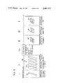
- FIG. 1is a somewhat diagrammatic fragmentary sectional view of a thin film p-n junction device constructed in accordance with the method of the present invention
- FIG. 2is a somewhat diagrammatic fragmentary sectional view of a thin film n-p junction device constructed in accordance with the method of the present invention
- FIG. 3is a diagrammatic representation of the method of the present invention, particularly as it would be practiced on a commercial scale;
- FIG. 4is a perspective view, partially broken away, of a preferred apparatus for magnetron sputtering a composition-graded multinary film according to the method of FIG. 3;
- FIG. 5is a fragmentary top plan view of one of the planar magnetron arrangements illustrated in FIG. 4, with the heat shields and anodes removed;
- FIG. 6is a vertical sectional view taken along the line 6--6 of FIG. 5;
- FIG. 7is a fragmentary top plan view of a planar magnetron arrangement constructed in accordance with another embodiment of the present invention.
- FIG. 8is a vertical sectional view taken along the line 8--8 of FIG. 7.
- the present inventioncomprises primarily an improvement on the method of the Chen and Mickelsen article and Mickelsen et al. U.S. Pat. No. 4,335,266, discussed above, and a planar magnetron apparatus for implementing the improved method.
- the cited article and patentare hereby incorporated by reference.
- FIG. 1a thin film p-n photovoltaic cell constructed in accordance with the method of the present invention, and generally designated 10.
- the cell 10comprises a pair of semiconductor layers or films 12 and 14 defining a p-n junction 16 therebetween.
- the layer 12is preferably a single phase p-type chalcopyrite film which is produced by magnetron sputtering techniques and initially defines a preselected composition gradient. The gradient is chosen to prevent the formation of nodules or other surface imperfections at the junction 16 and may be altered or eliminated by subsequent heat treatment, if desired.
- the layer 14is preferably CdS.
- the layers 12 and 14are positioned between a base contact 18 and an upper contact grid 20.
- the base contact 18is itself superimposed over a substrate 22, and the cell is covered with an anti-reflective (AR) coating 24.
- ARanti-reflective
- FIG. 2illustrates an alternative form of device constructed according to the method of the present invention, generally designated 26.
- the cell 26comprises an n-type semiconductor layer 28 and a p-type chalcopyrite layer 30 forming an n-p junction 32.
- the layers 28 and 30are positioned between a base contact grid 34 and an upper contact layer 36.
- the contact grid 34is formed on a transparent substrate 38 through which incident radiation (h ⁇ ) enters the cell 26.
- the cells 10 and 26are functionally similar; however, the various layers and contacts of the cells are applied to the substrates in different orders.
- the novel process and apparatus of the present inventionwhich relates to formation of one of the semi-conductor layers, will be discussed specifically in relation to the cell 10 with the understanding that it also applies generally to the cell 26.
- the illustrations of the cells 10 and 26, respectivelyare representative of prior art photovoltaic cells as well as the cells of the present invention.
- the cells 10 and 26differ from the prior art primarily in the nature of the layers 12 and 30, respectively, and the process by which they are formed. Because the layers 12 and 30 are formed by the novel magnetron sputtering method of the present invention, they are very high in quality, can be given virtually any desired composition gradient, and can be adapted to suit the requirements of virtually any cell.
- the semiconductor layer 12may be made of a chalcopyrite Cu-ternary material, such as CuInSe 2 , and has a composition which initially varies as a function of film depth.
- the layer 12extends from a Cu-enriched region adjacent the base contact 18 to a relatively Cu-deficient region at the junction 16, giving it a low resistivity at the base contact and a relatively high resistivity at the junction.
- the Cu concentration within the layer 12varies smoothly and continuously as a function of depth, ranging between values which would yield sheet resistivities of between 0.5K ohms per square and 10 3 K ohms per square, if formed in sheets 2 to 3 microns thick.
- the layer 12is deposited in two steps to produce a composition profile which is a step function of film depth.
- the composition profileis similar to concept to that disclosed by Chen and Mickelsen, but can be more accurately and economically produced by the method disclosed herein.
- the layercan then be heat treated to smooth out the profile and give the material a desired chalcopyrite structure.
- an initial deficiency of Cuis provided at the surface of the layer 12 which later forms the junction 16. This deficiency enhances the performance of the cell 10, even if the layer 12 is subsequently heated to diffuse the constituent elements therein.
- the highest quality CuInSe 2 cells produced by the applicants hereinhave been heat treated until the layers 12 were macroscopically homogeneous, in the sense that any inhomogeneity was so small that it could not be detected by conventional Auger mass spectroscopy.
- the layers produced in this waymight possess an inhomogeneity or other characteristic film structure at doping levels, i.e., at levels involving concentration gradients between approximately 10 -17 and 10 -19 atoms per cm -4 , they do not suffer from the adverse effects described by Chen and Mickelsen.
- the layer 12were initially deposited as a homogeneous layer of CuInSe 2 having the same overall composition, and thus a relatively low resistivity, a great many adverse surface conditions would exist at the interface with the CdS layer 14.
- CuInSe 2 films having uniform resistivities less than approximately 50K ohms per square at the time of depositionhave been found to exhibit a large number of Cu nodules when exposed to CdS, causing photovoltaic cells made from them to suffer from low efficiency. Precise control of the deposition process as a function of layer depth is thus necessary to maximize cell efficiency and to assure consistency in cell production.
- FIG. 3illustrates a manufacturing process having deposition stages I through V, the process being adapted for use on a large commercial scale.
- the substrate 22is preferably a sheet of polycrystalline alumina (A1 2 0 3 ) approximately 0.025 inches thick. However, glass, enameled steel, metallic foil or other suitable material may also be used. In the case of the n-p cell 26 of FIG. 2, the substrate 38 is made of glass or similar material permitting transmission of light therethrough.
- the base contact 18may be made of molybdenum (Mo), a Mo/Au alloy, or more conventional nickel or graphite materials, and is deposited by magnetron sputtering or other suitable technique onto the substrate 22.
- This stepshown at stage I of FIG. 3, involves the use of one or more magnetron cathodes 40 which are shown diagrammatically in FIG. 3.
- the cathodes 40may be of conventional construction and may operate in the same partial pressure of argon as the sputtering arrangements described below in connection with stage II.
- the layer 12is applied over the base contact 18 using magnetron sputtering techniques.
- the layeris initially provided with a composition gradient, either by varying the relative sputtering rates of the different constituent elements over time or passing the substrate over a number of magnetron sputtering arrangements 44 which are adapted to sputter the constituent elements in different preselected proportions.
- An apparatus 46 containing the sputtering arrangements 44is shown diagrammatically in FIG. 3 and illustrated in more detail in FIG. 4.
- the sputtering rates of the individual elementscan be controlled within a few parts per million (ppm).
- the thickness of the layer 12is preferably on the order of 3 microns, and the portion of the layer furthest from the base contact initially has a relatively high resistivity (i.e., a Cu/In ratio which would yield a sheet resistivity 50K ohms per square if formed in a sheet 2 to 3 microns thick).
- stage IIathe deposition of stage II is followed by an optional heat treatment of the deposited film within a furnace to enhance its molecular structure and aid in diffusion.
- the constituent elementscan be sputtered at room temperature in stage II to produce an amorphous mix having a specific concentration profile, and subsequently heated in stage IIa to produce a desired film structure and final concentration profile.
- the heat treatmentalso drives out any excess concentration of one or more volatile constituent elements of the film. Temperatures of 350° to 500° Celsius, continued for a period between 15 minutes and 2 hours, are suitable in the case of CuInSe 2 .
- heat treatmentcan be conducted in a reactive atmosphere containing one of the constituent elements of the material, for the purpose of supplementing the concentration of the element in the film.
- the reactive atmosphere used in connection with CuInSe 2may contain H 2 Se, eliminating any deficiency of Se in the film.
- H 2 Se moleculesbreak apart upon contact with the deposited layer, causing Se atoms to be absorbed into the film. This process proceeds rapidly because Se diffuses well at the relevant temperatures.
- the constituent elements of the layer 12may be desirable to sputter the constituent elements of the layer 12 (stage II) at a temperature great enough to form a chalcopyrite molecular structure at the deposition surface. Subsequently, stress within the layer can be relieved by heat treatment at a temperature lower than that required to produce diffusion. A temperature of 100° Celsius, or less, is suitable for this purpose.
- the n-type layer 14is applied at stage III of FIG. 3, by thermal evaporation or other suitable means, to a depth of approximately 2 to 3 microns.
- the technique of thermal evaporationis adequate because the n-type layer 14 is a homogeneous layer of uniform concentration.
- CdS or other suitable n-type materialcan be placed in a conventional evaporation boat 48 and essentially boiled to produce a stream of CdS vapor. Because the portion of the layer 12 adjoining the n-type CdS layer was relatively Cu-deficient when originally deposited, Cu nodules or other surface defects are not produced in any substantial number at the p-n junction.
- the contact grid 20is preferably made of aluminum applied to the layer 14 by conventional throughmask vacuum deposition techniques from an evaporation boat 50.
- the grid linesare applied to a depth of approximately 2 microns and are approximately 25 microns wide. Satisfactory results are achieved with 5 to 10 such lines per centimeter.
- Aluminumis commonly used for this purpose because it exhibits both high conductivity and excellent ohmic contact characteristics.
- a materialsuch as indium chromium or molybdenum may be used to form an interface between the layer 14 and a superimposed electrode material such as copper, silver or nickel.
- the coatingmay comprise any suitable transparent material having a low reflectivity with respect to solar radiation.
- Conventional AR coatingsinclude oxides of silicon, aluminum, indium, tin, and tantalum.
- the Ar coatingmay be applied by thermal evaporation from a boat 52, or by any other suitable technique.
- Stages III, IV and V of FIG. 3represent conventional processes which are well known in the semiconductor field. The details of the processes will therefore not be discussed herein.
- stage Vit may be desirable to subject the substrate 22 to a separate low temperature annealing step after stage V.
- the annealing stepis preferably accomplished at no more than 100° C., and may take place either in air or in a vacuum. Annealing after stage V can enhance the structure of either semiconductor layer, improve the semiconductor junction and improve the interface between the contacts and the semiconductor layers.
- the photovoltaic cell 26is manufactured using the method steps of FIG. 3, but in essentially the opposite order.
- the contact grid 34is first deposited on the transparent substrate 38 in the manner of the grid 20 of the cell 10.
- the layer 28, the layer 30, and the upper contact layer 36are then applied in the manner of the layer 14, the layer 12, and the contact 18, but in the reverse order.
- the initial composition gradient of the layer 30is also reversed from that of the layer 12 to place the relatively Cu-deficient region adjacent the layer 28.
- the method and apparatus of the present inventionis uniquely adapted to production of the cell 26 because the layer 30 is applied after the other semiconductor layer 28. Since the magnetron sputtering method of the present invention can often be performed at lower temperatures than conventional deposition and diffusion processes, the layer 30 can be deposited by the method without damage to the layer 28. Of course, high temperature heat treatment would usually not be suitable for use in producing the cell 26 because it might damage the other elements of the cell and the n-p junction within the cell.
- a significant aspect of the present inventioninvolves accomplishing the magnetron sputtering process of stage II with the apparatus 46 of FIG. 4.
- the apparatus 46comprises a plurality of the magnetron sputtering arrangements 44 positioned side-by-side to deposit the constituent elements of the layer 12 onto a series of substrates 22 passed transversely over the apparatus.
- Each of the sputtering arrangementssimultaneously sputters two or more constituent elements of the layer 12 in preselected proportions.
- Eachis supplied with electric power by a plurality of power lines illustrated diagrammatically at 54, the power being applied through fluid conduits 56 which carry water or other cooling fluid through the arrangements 44.
- the substratesare conveyed over the sputtering arrangements by a number of wheels 58 positioned between the sputtering arrangements.
- the wheelsmay be driven for rotation intermittently or at a uniform rate by a suitable drive means, such as a chain and sprocket mechanism 60 and a series of drive shafts 62.
- the undersides of the substratesreceive sputtered material from each of the magnetron sputtering arrangements 44 as they pass thereover.
- the sputtering arrangements 44can be suspended upside-down to sputter downwardly as the substrates are conveyed thereunder.
- the sputtering contributions of the arrangements 44are cumulative, building upon each other to form the chalcopyrite layer 12.
- the "as deposited" layer 12thus has a depthwise composition gradient which reflects the relative proportions of constituent elements sputtered by the various arrangements. Individual control of the proportion of elements sputtered by each arrangement, in conjunction with control of the rate at which the substrates are conveyed, permit virtually any desired composition gradient to be produced in the layer 12.
- the apparatus 46permits the layer 12 to be deposited in a continuous process suitable for use on a commercial scale.
- the arrangement 44comprises three magnetically-enhanced sputtering structures or "racetracks", designated 64, 66, and 68, respectively.
- Each of the racetracksforms a continuous loop extending about a common axis 70, and in that sense may be described as being "concentric” with each other.
- the racetracksare individual planar magnetrons, separately controllable as to the rates at which the corresponding constituent elements are sputtered therefrom. They are combined in the concentric configuration of FIGS. 5 and 6 to produce a narrow device able to sputter the constituent elements of the layer 12 in any desired proportions.
- Each racetrackcomprises a source 72 containing at least one of the constituent elements of the layer 12, and a plurality of bar magnets 74.
- the sources 72may be made of Cu, In, and Se, respectively.
- the sourcesare essentially coextensive with the corresponding racetracks and may comprise the appropriate materials in bar or tile form.
- Each sourceis supported by a plurality of holding blocks 76 of aluminum or other suitable non-magnetic material.
- the fluid conduits 56 described above in relation to FIG. 4pass through the holding blocks in the direction of the racetrack loop, and the magnets 74 pass through the blocks in a transverse direction.
- Each source 72 and the corresponding holding blocks 76are sandwiched between a pair of vertical pole pieces 80 extending continuously about the racetrack loop.
- the pole piecesabut opposite poles of the magnets 74 to conduct the lines of magnetic force to an area 82 directly above the source.
- the pole pieces 80are preferably made of mild steel or other suitable ferromagnetic material.
- Each of the racetracksalso has a base plate 84 supported by a plurality of legs 86 positioned on insulator bases 88.
- the base plate 84is preferably made of a ferromagnetic material and extends between the lower ends of the pole pieces 80 to complete the magnetic circuit therebetween. An external magnetic field is thus produced only in the area 82 above the source 72, limiting sputtering activity to the source 72.
- the base plates 84 of the racetracks 66 and 68are provided with enlarged openings 90 for reception of the legs 86 of one or more of the other racetracks.
- the openings 90are substantially greater in diameter than the legs 86, preventing electrical contact between the racetracks in this region.
- the base plates 84are spaced vertically from one another and the racetracks 64 through 68 are spaced apart laterally, causing the racetracks to be in electrical isolation from each other and from a floor or other supporting surface 92.
- Each of the racetracksthus comprises a separate planar magnetron which is effectively isolated both magnetically and electrically from the others.
- Electrical power for sputteringis introduced to the racetracks through the fluid conduits 56, each of the conduits 56 being connected to one of the power lines 54 of FIG. 4 to apply a preselected level of electric power to the corresponding source 72.
- the racetrackscomprise separate cathodes for the application of electric power to the sputtering system.
- a plurality of auxiliary cooling lines 94extending about the axis 70 at locations between the racetracks, act as anodes for the system.
- the magnetron sputtering arrangements 44can be up to approximately eight feet long for use on a commercial scale, enabling them to be used with a substrate up to approximately eight feet wide.
- the arrangements 44may then be approximately ten inches wide, with each strip of source material being one inch wide.
- the lower surface of the substrate 22may be spaced approximately 21/2 to 4 inches above the magnetron arrangements, permitting the sputtered elements to be mixed through dispersion without reducing the rate of deposition.
- one or more of the sputtering arrangements 44are positioned within a chamber (not shown) which is evacuated and back-filled with argon or other suitable gas to a very low pressure.
- Electric poweris supplied to the cathodes of the racetracks 64 through 68 at individually controllable levels to cause the onset of magnetron sputtering.
- the negative potential supplied to a particular cathodedrives electrons out of the corresponding source 72 in an upward direction. The electrons are trapped above the source by the magnetic field and collide with argon atoms to produce a high energy plasma.
- Ar+ ionsare drawn from the plasma by the negative potential of the cathode and impact the source material with a force sufficient to jar loose atoms of the source material.
- sputtered atomspossess substantial kinetic energy and are directed essentially upwardly from the source. They are uncharged and virtually unaffected by either the potential of the source or the magnetic field within the area 82, permitting them to retain high kinetic energy as they pass upwardly to the surface of the substrate 22. The sputtered atoms impact the substrate with substantial kinetic energy, often giving them sufficient mobility within the deposited layer to assume favored positions in its structure.
- Proper control of sputtering rates from the sources 72can produce a single phase layer of a multinary semiconductive material with a preselected composition gradient or "profile". The gradient is determined by the relative levels of electric power applied to the sources over time.
- the sputtered atomshave sufficient kinetic and thermal energies to form a polycrystalline layer of the semiconductive material.
- elemental co-sputtering of Cu, In and Se at temperatures of at least 250 degrees Celsiuscan produce a single phase chalcopyrite film of CuInSe 2 .
- Crystal growthis preferably columnar in shape and produces very few grain boundaries across the direction of carrier travel. Due to the difficulty of controlling a sputtering source of pure Se in the solid phase, this process is most viable when Se is sputtered from a liquid source. However, the other elements must then be sputtered very rapidly to match the rate of Se deposition. This process is suitable for rapid, large scale commercial deposition, but is not easily scaled down to the laboratory level.
- the elementscan be sputtered at room temperature, yielding an amorphous mix of atoms which must be heat treated if a chalcopyrite structure is desired.
- the atomic composition of the layer, as deposited,remains a function of the electric power to the cathodes, permitting the initial composition gradient to be carefully controlled.
- the initial composition of the layer 12is graded either by varying the electrical power levels to the cathodes or providing a number of magnetron sputtering arrangements 44, as shown in FIG. 4, with the proportions of sputtered elements differing between the arrangements. If the power levels are varied over time, the substrate 22 may remain stationary above the sputtering arrangement 44; however, in the configuration of FIG. 4, the substrate is conveyed over the sputtering arrangements.
- the atoms sputtered from the sources 72 of a particular sputtering arrangementare effectively mixed in the distance between the sources and the substrate 22.
- the atomsare sputtered from the sources at random angles with the vertical, causing the flows of sputtered atoms to fan out and intermix on the way to the substrate.
- the racetracks 64 through 68are narrow and closely spaced for this purpose.
- a heated shield 96is angled inwardly from the periphery of the racetrack 68 to reflect sputtered atoms toward the inner two racetracks, aiding in mixing the atoms.
- the Se atomsare by far the most mobile of the sputtered atoms and are thus the logical choice for placement in the outer racetrack 68. They diffuse well to all points between the substrate 22 and the sputtering arrangement 44.
- One or more of the sources 72may be an alloy of two or more constituent elements of the layer 12.
- the source of the racetrack 64may be an alloy of Cu and In for sputtering the two elements in a preselected fixed proportion determined by the proportion of Cu to In in the alloy.
- the racetrack 66can then be used to sputter either Cu or In, permitting variation of the ratio of Cu to In in the sputtered layer by varying the power to the cathodes, and the racetrack 68 can be used to sputter Se.
- the racetrack 66can be eliminated and a number of magnetron arrangements incorporating different alloys of Cu and In can be placed side-by-side in the manner of the apparatus 46 to sputter the constituent elements in a set of preselected fixed proportions determined by the proportions of elements in the targets.
- the constituents of the layer 12when one of the constituents of the layer 12 is difficult to sputter in isolation it can sometimes be sputtered with greater control from a stable alloy containing another element of the layer.
- Seis a semi-metal which is difficult to controllably sputter from the solid phase because of its low melting point. Under sputtering conditions, it tends to evaporate as it sputters, drastically reducing the level of control over film composition.
- Secan be sputtered in precisely controlled stoichiometric ratios from certain stable selenium alloys, including Cu 2 Se and In 2 Se 3 .
- the sources of the racetracks 64 and 66 used to deposit CuInSe 2may be made of Cu 2 Se and In 2 Se 3 , respectively, permitting the Cu to In ratio to be controlled by the power to the two sources.
- the racetrack 68can be eliminated or can be adapted to sputter Cu or In, alone. The latter configuration permits control of the proportion of each element in the film, including Se.
- a further possibility for depositing CuInSe 2is to sputter Cu and In, as described above, while depositing Se by thermal evaporation or other conventional means. Mixing of evaporated Se with the Cu-In vapor stream can be enhanced by using heated shields similar to the shield 96 of the arrangement 44. This method is feasible because Se is a very good diffuser. However, it does not produce a film of the quality achieved when Se is sputtered from stable alloys.
- CuInSe 2 /CdS solar cellshave been fabricated experimentally from alloy targets containing Se.
- the alloys used in depositing the CuInSe 2 layerwere Cu 2 Se and In 2 Se 3 .
- Sputteringwas accomplished with side-by-side dc planar magnetrons of conventional design, having 4-inch round targets approximately 1/4-inch thick. Deposition took place at room temperature (no substrate heat), in an atmosphere of argon at a pressure of approximately 8 millitorr. The applied voltage was between -450 and -500 volts DC and current was approximately 1/4 to 1/2 ampere per target. Under these conditions, material would be deposited at a rate of approximately 10 angstroms per second on a stationary substrate positioned above the magnetron targets.
- the resultant filmwas an amorphous mix of Cu, In and Se, in relative proportions determined by the electrical power to the targets.
- the filmwas deposited on a one-inch square alumina substrate to a total thickness of between 1.5 and 2 micrometers.
- the substratewas prepared with a suitable sputtered base contact prior to deposition.
- a sharp gradation in the initial Cu to In ratiosimilar to that described by Chen and Mickelsen, was provided in the CuInSe 2 layer by depositing the film in two layers of different composition.
- the first layerwas deposited to approximately two-thirds of the total film thickness, at a Cu/In ratio of 1.02. It was therefore a p-type layer of low resistivity.
- a second layerwas deposited with a Cu/In ratio of 0.675 by increasing the power to the In 2 Se 3 target.
- the resulting materialwas n-type and relatively high in resistivity.
- the filmwas heat treated to convert the amorphous mixture to crystalline (chalcopyrite) CuInSe 2 .
- Heat treatmentalso caused diffusion within the film to remove the sharp composition gradient and homogenize the film at a macroscopic level.
- the resulting filmis a high quality p-type CuInSe 2 film having the desired chalcopyrite structure and very few surface defects.
- the filmmay be inhomogenous at doping levels, but has been found to be entirely homogeneous as far as can be determined with conventional Auger mass spectroscopy.
- the "as deposited" filmhad an overall Se concentration at least equal to the stoichiometric abundance of Se in CuInSe 2
- heat treatmentwas accomplished in argon gas with approximately one percent H 2 Se.
- an atmosphere of pure argon, or argon and H 2would be equally suitable for this purpose.
- the heat treatmentwas accomplished at 400 degrees Celsius, with a 20 minute heat-up to that temperature. The temperature of 400 degrees was maintained for two hours, followed by a slow cooling.
- the alloy targets used to sputter the sample CuInSe 2 filmswere fabricated by melting the respective constituent elements together into the desired shape.
- the Cu 2 Se targetwas formed by melting two parts of copper together with one part of selenium and cooling the mixture.
- the In 2 Se 3 targetwas formed by melting two parts of Indium together with three parts of selenium.
- the targetscould also be fabricated using conventional hot pressing techniques.
- the one-inch square solar cells prepared in the manner described aboveexhibit efficiencies of approximately six percent.
- the cellshave the largest active area of any CuInSe 2 /CdS cells known to applicants, and represent the highest reported efficiency for such cells produced by a sputtering process. This is true despite the fact that a great many parameters in the process have not yet been fully optimized, including parameters related to target fabrication, heat treatment, CdS deposition and grid line formation.
- the disclosed cellswere also made with discrete planar magnetrons positioned side-by-side in a deposition environment, rather than with the concentric racetrack structure of the present invention. It is therefore possible to further improve the process by which the cells are made, for the purpose of improving cell efficiency.
- the viability of the process of the present invention for producing high quality solar cells in a commercially scalable mannerhas been clearly shown.
- the sputtering arrangement 144is suitable for use in the side-by-side configuration illustrated in FIG. 4 with regard to the arrangement 44, the principal difference being the source structure of the arrangement 144. That is, Cu and In are sputtered from a single racetrack 146 having a source comprising a plurality of Cu tiles or plates 148 alternated with In tiles or plates 150. A second racetrack 152 extends about the racetrack 146 for sputtering Se. A pair of elongated Se sources 154 extends lengthwise along the racetrack 152 on either side of the racetrack 146.
- the end portions 157 of the racetrack 152include a pair of graphite plates in place of the source material. Graphite is provided at these locations to eliminate undue sputtering of Se at the ends of the arrangement 144. Graphite is a very difficult element to sputter and will remain undisturbed under the conditions of the present method.
- the sources 154 and the tiles 148 and 150are supported on suitable holding blocks 176 which are similar to the holding blocks 76 described above in relation to the apparatus 44.
- cooling water and a negative electrical potentialare applied to the two racetracks through corresponding cooling lines 156, and magnetic fields are established above the sources by a plurality of bar magnets 174 and pole pieces 180.
- the pole piecesextend continuously about the racetracks 146 and 152 in the manner of the arrangement 44, with the magnets positioned at regular intervals therealong.
- the racetracksare also provided with base plates 184, legs 186 and insulator bases 188 for supporting the racetracks in an electrically isolated condition. These elements are similar to those described above in relation to the sputtering arrangement 44.
- Auxiliary cooling lines 194provide an electrical anode for the completion of the electric circuit of the system, and a heated reflector shield 196 directs Se toward the substrate.
- the sputtering arrangement 144can be used in the side-by-side arrangement of FIG. 4 in essentially the same manner as the arrangement 44.
- the proportion of Cu to In sputtered from the arrangement 144depends upon the relative abundance of the tiles 148 and 150 in the racetrack 146.
- the alternating tile arrangementnot only provides excellent mixing of the sputtered atoms of Cu and In, but also permits the ratio of sputtered Cu and In atoms to be easily changed by varying the relative abundance of the tiles 148 and 150. In cases where the number of tiles is altered for this purpose, the pattern of tiles may, of course, no longer be strictly alternating.
- the sputtering arrangement 144may be dimensioned approximately the same as the sputtering arrangement 44, with the exception that the width of the arrangement will be somewhat less because one racetrack has been eliminated.
- the tiles 148 and 150 of the racetrack 146are preferably approximately 1/2 inch square.
- the sources 72 at the curved end portions of the racetracksmay be replaced by graphite plates similar to the end portions 157 of the sputtering arrangement 144. This would minimize material loss from the ends of the sources and enhance the uniformity of distribution of sputtered material. However, it would also reduce the maximum width of substrate with which it can be used.
- the substitution of graphite or other non-sputtering material at the ends of the racetracksthus remains an option which can be used in some exacting circumstances, but which may not be desirable in many large scale production environments.
- the magnets 74 and 174may be of any conventional type, including electromagnets.
- the power applied to the various cathodes or racetracks described abovecan take the form of either ac or dc power. Generally, dc power is more electrically efficient while high frequency ac power is required when sputtering insulators.
- the source materialscan be sputtered from a molten state, with a very substantial increase in sputtering rate. To accomplish this, power to the cathodes can be greatly increased or a thermal insulator can be placed between the sources and the cooling lines 78 or 178.
- Magnetic field strengthapproximately 200 gauss at a distance of one inch above the source
- Resultant deposition ratesapproximately 4,000 A per minute per cathode (at 21/2 inches from source), or much higher when sputtering from the liquid phase.
- Rate of substrate travel2 feet per minute
- the method and apparatus of the present inventionis applicable generally to the production of composition-graded layers of semiconductor materials in the class of I-III-VI 2 ternary chalcopyrite compounds, as well as some related quaternary materials.
- the ternary chalcopyrite compounds other than CuInSe 2 to which the present invention relatesinclude, without limitation: CuGaSe 2 , CuInS 2 , CuInTe 2 , AgInS 2 , AgInSe 2 , AgInTe 2 , AgGaSe 2 and AgGaTe 2 .
Landscapes
- Chemical & Material Sciences (AREA)
- Chemical Kinetics & Catalysis (AREA)
- Engineering & Computer Science (AREA)
- Materials Engineering (AREA)
- Mechanical Engineering (AREA)
- Metallurgy (AREA)
- Organic Chemistry (AREA)
- Photovoltaic Devices (AREA)
Abstract
Description
Claims (13)
Priority Applications (1)
| Application Number | Priority Date | Filing Date | Title |
|---|---|---|---|
| US06/470,418US4465575A (en) | 1981-09-21 | 1983-02-28 | Method for forming photovoltaic cells employing multinary semiconductor films |
Applications Claiming Priority (2)
| Application Number | Priority Date | Filing Date | Title |
|---|---|---|---|
| US30452081A | 1981-09-21 | 1981-09-21 | |
| US06/470,418US4465575A (en) | 1981-09-21 | 1983-02-28 | Method for forming photovoltaic cells employing multinary semiconductor films |
Related Parent Applications (1)
| Application Number | Title | Priority Date | Filing Date |
|---|---|---|---|
| US30452081AContinuation-In-Part | 1981-09-21 | 1981-09-21 |
Publications (1)
| Publication Number | Publication Date |
|---|---|
| US4465575Atrue US4465575A (en) | 1984-08-14 |
Family
ID=26974070
Family Applications (1)
| Application Number | Title | Priority Date | Filing Date |
|---|---|---|---|
| US06/470,418Expired - LifetimeUS4465575A (en) | 1981-09-21 | 1983-02-28 | Method for forming photovoltaic cells employing multinary semiconductor films |
Country Status (1)
| Country | Link |
|---|---|
| US (1) | US4465575A (en) |
Cited By (146)
| Publication number | Priority date | Publication date | Assignee | Title |
|---|---|---|---|---|
| EP0162642A1 (en)* | 1984-05-17 | 1985-11-27 | Varian Associates, Inc. | Magnetron sputter device using the same pole piece for coupling separate confining magnetic field to separate targets subject to separate discharges |
| US4606806A (en)* | 1984-05-17 | 1986-08-19 | Varian Associates, Inc. | Magnetron sputter device having planar and curved targets |
| US4622121A (en)* | 1984-04-19 | 1986-11-11 | Balzers Aktiengesellschaft | Apparatus for coating materials by cathode sputtering |
| EP0211529A1 (en)* | 1985-07-16 | 1987-02-25 | Atlantic Richfield Company | Method for forming CuInSe2 films |
| EP0265105A1 (en)* | 1986-10-06 | 1988-04-27 | Mcnc | A method of etching a substrate |
| US4761218A (en)* | 1984-05-17 | 1988-08-02 | Varian Associates, Inc. | Sputter coating source having plural target rings |
| US4769086A (en)* | 1987-01-13 | 1988-09-06 | Atlantic Richfield Company | Thin film solar cell with nickel back |
| US4798660A (en)* | 1985-07-16 | 1989-01-17 | Atlantic Richfield Company | Method for forming Cu In Se2 films |
| US4818357A (en)* | 1987-05-06 | 1989-04-04 | Brown University Research Foundation | Method and apparatus for sputter deposition of a semiconductor homojunction and semiconductor homojunction products created by same |
| US4915745A (en)* | 1988-09-22 | 1990-04-10 | Atlantic Richfield Company | Thin film solar cell and method of making |
| US5028274A (en)* | 1989-06-07 | 1991-07-02 | International Solar Electric Technology, Inc. | Group I-III-VI2 semiconductor films for solar cell application |
| US5045166A (en)* | 1990-05-21 | 1991-09-03 | Mcnc | Magnetron method and apparatus for producing high density ionic gas discharge |
| US5045409A (en)* | 1987-11-27 | 1991-09-03 | Atlantic Richfield Company | Process for making thin film solar cell |
| US5078803A (en)* | 1989-09-22 | 1992-01-07 | Siemens Solar Industries L.P. | Solar cells incorporating transparent electrodes comprising hazy zinc oxide |
| WO1993023881A1 (en)* | 1992-05-12 | 1993-11-25 | Solar Cells, Inc. | Process and apparatus for making photovoltaic devices and resultant product |
| US5356839A (en)* | 1993-04-12 | 1994-10-18 | Midwest Research Institute | Enhanced quality thin film Cu(In,Ga)Se2 for semiconductor device applications by vapor-phase recrystallization |
| US5393675A (en)* | 1993-05-10 | 1995-02-28 | The University Of Toledo | Process for RF sputtering of cadmium telluride photovoltaic cell |
| US5405517A (en)* | 1993-12-06 | 1995-04-11 | Curtis M. Lampkin | Magnetron sputtering method and apparatus for compound thin films |
| US5422304A (en)* | 1991-09-27 | 1995-06-06 | Matsushita Electric Industrial Co., Ltd. | Method for producing a thin film, and a semiconductor device having the thin film |
| US5436204A (en)* | 1993-04-12 | 1995-07-25 | Midwest Research Institute | Recrystallization method to selenization of thin-film Cu(In,Ga)Se2 for semiconductor device applications |
| US5439575A (en)* | 1988-06-30 | 1995-08-08 | Board Of Trustees Of The University Of Illinois | Hybrid method for depositing semi-conductive materials |
| US5445847A (en)* | 1992-05-19 | 1995-08-29 | Matsushita Electric Industrial Co., Ltd. | Method for preparing chalcopyrite-type compound |
| AU668596B2 (en)* | 1992-11-06 | 1996-05-09 | Joslyn Manufacturing Company | High strength anchor |
| US5567469A (en)* | 1992-10-30 | 1996-10-22 | Matsuhita Electric Co., Ltd. | Process for producing chalcopyrite type compound thin film |
| US5645699A (en)* | 1994-09-06 | 1997-07-08 | The Boc Group, Inc. | Dual cylindrical target magnetron with multiple anodes |
| US5985691A (en)* | 1997-05-16 | 1999-11-16 | International Solar Electric Technology, Inc. | Method of making compound semiconductor films and making related electronic devices |
| US6048442A (en)* | 1996-10-25 | 2000-04-11 | Showa Shell Sekiyu K.K. | Method for producing thin-film solar cell and equipment for producing the same |
| US6268014B1 (en) | 1997-10-02 | 2001-07-31 | Chris Eberspacher | Method for forming solar cell materials from particulars |
| US6309516B1 (en) | 1999-05-07 | 2001-10-30 | Seagate Technology Llc | Method and apparatus for metal allot sputtering |
| US6323417B1 (en) | 1998-09-29 | 2001-11-27 | Lockheed Martin Corporation | Method of making I-III-VI semiconductor materials for use in photovoltaic cells |
| US6328856B1 (en) | 1999-08-04 | 2001-12-11 | Seagate Technology Llc | Method and apparatus for multilayer film deposition utilizing rotating multiple magnetron cathode device |
| US6518086B2 (en) | 1999-11-16 | 2003-02-11 | Midwest Research Institute | Processing approach towards the formation of thin-film Cu(In,Ga)Se2 |
| US20040188242A1 (en)* | 2003-03-28 | 2004-09-30 | Ga-Lane Chen | Method of manufacturing electromagnetic interference shield |
| US20050016835A1 (en)* | 1998-12-21 | 2005-01-27 | Cardinal Cg Company | Soil-resistant coating for glass surfaces |
| US20050026002A1 (en)* | 2003-06-24 | 2005-02-03 | Klaus Hartig | Concentration-modulated coatings |
| US20050109392A1 (en)* | 2002-09-30 | 2005-05-26 | Hollars Dennis R. | Manufacturing apparatus and method for large-scale production of thin-film solar cells |
| US20050233899A1 (en)* | 2001-12-21 | 2005-10-20 | Toshiaki Anzaki | Member having photocatalytic function and method for manufacture thereof |
| US20060096635A1 (en)* | 2004-11-10 | 2006-05-11 | Daystar Technologies, Inc. | Pallet based system for forming thin-film solar cells |
| US20060219288A1 (en)* | 2004-11-10 | 2006-10-05 | Daystar Technologies, Inc. | Process and photovoltaic device using an akali-containing layer |
| US20070237968A1 (en)* | 2004-12-06 | 2007-10-11 | Nippon Sheet Glass Company, Limited | Glass Member Having Photocatalytic Function and Heat Reflecting Function and Double Paned Glass Including The Same |
| US20070248756A1 (en)* | 2006-04-19 | 2007-10-25 | Cardinal Cg Company | Opposed functional coatings having comparable single surface reflectances |
| US7294404B2 (en) | 2003-12-22 | 2007-11-13 | Cardinal Cg Company | Graded photocatalytic coatings |
| CN100383982C (en)* | 2004-06-14 | 2008-04-23 | 王东生 | Multi-absorbing-layer solar battery and manufacturing method thereof |
| US20080092953A1 (en)* | 2006-05-15 | 2008-04-24 | Stion Corporation | Method and structure for thin film photovoltaic materials using bulk semiconductor materials |
| US20080108194A1 (en)* | 2005-08-31 | 2008-05-08 | Szu-Yu Wang | Memory device and manufacturing method thereof |
| US20080241409A1 (en)* | 2007-03-30 | 2008-10-02 | Guo G X | Deposition system with improved material utilization |
| US20090017605A1 (en)* | 2007-07-10 | 2009-01-15 | Stion Corporation | Methods for doping nanostructured materials and nanostructured thin films |
| US20090068503A1 (en)* | 2007-08-23 | 2009-03-12 | Mutsuki Yamazaki | Sputtering apparatus |
| US20090087370A1 (en)* | 2007-09-28 | 2009-04-02 | Stion Corporation | Method and material for purifying iron disilicide for photovoltaic application |
| US20090087939A1 (en)* | 2007-09-28 | 2009-04-02 | Stion Corporation | Column structure thin film material using metal oxide bearing semiconductor material for solar cell devices |
| US20090117718A1 (en)* | 2007-06-29 | 2009-05-07 | Stion Corporation | Methods for infusing one or more materials into nano-voids if nanoporous or nanostructured materials |
| US20090113726A1 (en)* | 2007-09-28 | 2009-05-07 | Cedric Ducros | Method for obtaining a hard surface at the nanoscale |
| US20090169723A1 (en)* | 2007-10-02 | 2009-07-02 | University Of Delaware | I-iii-vi2 photovoltaic absorber layers |
| US20090223551A1 (en)* | 2008-03-04 | 2009-09-10 | Solexant Corp. | Process for making solar cells |
| US7604865B2 (en) | 2004-07-12 | 2009-10-20 | Cardinal Cg Company | Low-maintenance coatings |
| US20100170566A1 (en)* | 2009-01-06 | 2010-07-08 | Arthur Don Harmala | Apparatus and method for manufacturing polymer solar cells |
| US20100247745A1 (en)* | 2007-09-12 | 2010-09-30 | Dominik Rudmann | Method for manufacturing a compound film |
| USD625695S1 (en) | 2008-10-14 | 2010-10-19 | Stion Corporation | Patterned thin film photovoltaic module |
| USD627696S1 (en) | 2009-07-01 | 2010-11-23 | Stion Corporation | Pin striped thin film solar module for recreational vehicle |
| USD628332S1 (en) | 2009-06-12 | 2010-11-30 | Stion Corporation | Pin striped thin film solar module for street lamp |
| USD632415S1 (en) | 2009-06-13 | 2011-02-08 | Stion Corporation | Pin striped thin film solar module for cluster lamp |
| WO2011019886A1 (en) | 2009-08-13 | 2011-02-17 | Dow Global Technologies, Inc. | A multi-layer laminate structure and manufacturing method |
| US20110048522A1 (en)* | 2009-08-26 | 2011-03-03 | Industrial Technology Research Institute | Solar cell |
| US20110067998A1 (en)* | 2009-09-20 | 2011-03-24 | Miasole | Method of making an electrically conductive cadmium sulfide sputtering target for photovoltaic manufacturing |
| WO2011037846A1 (en)* | 2009-09-24 | 2011-03-31 | The Government Of The United States Of America, As Represented By The Secretary Of The Navy | Copper indium gallium selenide (cigs) thin films with composition controlled by co-sputtering |
| US7923114B2 (en) | 2004-12-03 | 2011-04-12 | Cardinal Cg Company | Hydrophilic coatings, methods for depositing hydrophilic coatings, and improved deposition technology for thin films |
| US20110100438A1 (en)* | 2009-11-04 | 2011-05-05 | Gaston Ryan S | Building integrated photovoltaic having injection molded component |
| US7939454B1 (en) | 2008-05-31 | 2011-05-10 | Stion Corporation | Module and lamination process for multijunction cells |
| US7943415B1 (en)* | 2010-10-27 | 2011-05-17 | Primestar Solar Inc. | Methods of sputtering cadmium sulfide layers for use in cadmium telluride based thin film photovoltaic devices |
| US20110162696A1 (en)* | 2010-01-05 | 2011-07-07 | Miasole | Photovoltaic materials with controllable zinc and sodium content and method of making thereof |
| US20110220183A1 (en)* | 2010-03-12 | 2011-09-15 | Dow Global Technologies Llc | Photovoltaic device |
| US8058092B2 (en) | 2007-09-28 | 2011-11-15 | Stion Corporation | Method and material for processing iron disilicide for photovoltaic application |
| US8067263B2 (en) | 2008-09-30 | 2011-11-29 | Stion Corporation | Thermal management and method for large scale processing of CIS and/or CIGS based thin films overlying glass substrates |
| US8075723B1 (en) | 2008-03-03 | 2011-12-13 | Stion Corporation | Laser separation method for manufacture of unit cells for thin film photovoltaic materials |
| US8092660B2 (en) | 2004-12-03 | 2012-01-10 | Cardinal Cg Company | Methods and equipment for depositing hydrophilic coatings, and deposition technologies for thin films |
| USD652262S1 (en) | 2009-06-23 | 2012-01-17 | Stion Corporation | Pin striped thin film solar module for cooler |
| US8105437B2 (en) | 2007-11-14 | 2012-01-31 | Stion Corporation | Method and system for large scale manufacture of thin film photovoltaic devices using multi-chamber configuration |
| US8134069B2 (en) | 2009-04-13 | 2012-03-13 | Miasole | Method and apparatus for controllable sodium delivery for thin film photovoltaic materials |
| WO2012033657A2 (en) | 2010-09-07 | 2012-03-15 | Dow Global Technologies Llc | Improved photovoltaic cell assembly |
| WO2012037191A2 (en) | 2010-09-17 | 2012-03-22 | Dow Global Technologies Llc | Improved photovoltaic cell assembly and method |
| WO2012044762A1 (en) | 2010-09-30 | 2012-04-05 | Dow Global Technologies Llc | An improved connector and electronic circuit assembly for improved wet insulation resistance |
| US20120090991A1 (en)* | 2010-04-21 | 2012-04-19 | Beijing Boe Optoelectronics Technology Co., Ltd. | Magnetron sputtering apparatus |
| US8168463B2 (en) | 2008-10-17 | 2012-05-01 | Stion Corporation | Zinc oxide film method and structure for CIGS cell |
| US8193028B2 (en) | 2008-10-06 | 2012-06-05 | Stion Corporation | Sulfide species treatment of thin film photovoltaic cell and manufacturing method |
| US8198122B2 (en) | 2008-09-29 | 2012-06-12 | Stion Corporation | Bulk chloride species treatment of thin film photovoltaic cell and manufacturing method |
| US8202407B1 (en) | 2009-01-06 | 2012-06-19 | Arthur Don Harmala | Apparatus and method for manufacturing polycarbonate solar cells |
| USD662040S1 (en) | 2009-06-12 | 2012-06-19 | Stion Corporation | Pin striped thin film solar module for garden lamp |
| USD662041S1 (en) | 2009-06-23 | 2012-06-19 | Stion Corporation | Pin striped thin film solar module for laptop personal computer |
| WO2012082613A2 (en) | 2010-12-17 | 2012-06-21 | Dow Global Technologies Llc | Improved photovoltaic device |
| WO2012082604A1 (en) | 2010-12-17 | 2012-06-21 | Dow Global Technologies Llc | Improved photovoltaic device |
| WO2012082608A2 (en) | 2010-12-17 | 2012-06-21 | Dow Global Technologies Llc | Improved photovoltaic device |
| US8207008B1 (en) | 2008-08-01 | 2012-06-26 | Stion Corporation | Affixing method and solar decal device using a thin film photovoltaic |
| WO2011050015A3 (en)* | 2009-10-21 | 2012-07-05 | Sunlight Photonics Inc. | Three-stage formation of thin-films for photovoltaic devices |
| US8236597B1 (en) | 2008-09-29 | 2012-08-07 | Stion Corporation | Bulk metal species treatment of thin film photovoltaic cell and manufacturing method |
| US8258000B2 (en) | 2008-09-29 | 2012-09-04 | Stion Corporation | Bulk sodium species treatment of thin film photovoltaic cell and manufacturing method |
| US8263494B2 (en) | 2010-01-25 | 2012-09-11 | Stion Corporation | Method for improved patterning accuracy for thin film photovoltaic panels |
| WO2012129356A2 (en) | 2011-03-22 | 2012-09-27 | Dow Global Technologies Llc | Improved photovoltaic sheathing element with one or more tabs |
| WO2012129355A2 (en) | 2011-03-22 | 2012-09-27 | Dow Global Technologies Llc | Improved photovoltaic building sheathing element with anti-slide features |
| US8287942B1 (en) | 2007-09-28 | 2012-10-16 | Stion Corporation | Method for manufacture of semiconductor bearing thin film material |
| WO2012154307A2 (en) | 2011-03-22 | 2012-11-15 | Dow Global Technologies Llc | Improved photovoltaic sheathing element with a flexible connector assembly |
| WO2012143858A3 (en)* | 2011-04-19 | 2012-12-27 | Flisom Ag | Thin-film photovoltaic device and fabrication method |
| US8344243B2 (en) | 2008-11-20 | 2013-01-01 | Stion Corporation | Method and structure for thin film photovoltaic cell using similar material junction |
| US8377736B2 (en) | 2008-10-02 | 2013-02-19 | Stion Corporation | System and method for transferring substrates in large scale processing of CIGS and/or CIS devices |
| US8383450B2 (en) | 2008-09-30 | 2013-02-26 | Stion Corporation | Large scale chemical bath system and method for cadmium sulfide processing of thin film photovoltaic materials |
| US8394662B1 (en) | 2008-09-29 | 2013-03-12 | Stion Corporation | Chloride species surface treatment of thin film photovoltaic cell and manufacturing method |
| US8398772B1 (en) | 2009-08-18 | 2013-03-19 | Stion Corporation | Method and structure for processing thin film PV cells with improved temperature uniformity |
| US8425739B1 (en) | 2008-09-30 | 2013-04-23 | Stion Corporation | In chamber sodium doping process and system for large scale cigs based thin film photovoltaic materials |
| US8436445B2 (en) | 2011-08-15 | 2013-05-07 | Stion Corporation | Method of manufacture of sodium doped CIGS/CIGSS absorber layers for high efficiency photovoltaic devices |
| US8435822B2 (en) | 2008-09-30 | 2013-05-07 | Stion Corporation | Patterning electrode materials free from berm structures for thin film photovoltaic cells |
| US8435826B1 (en) | 2008-10-06 | 2013-05-07 | Stion Corporation | Bulk sulfide species treatment of thin film photovoltaic cell and manufacturing method |
| US8440903B1 (en) | 2008-02-21 | 2013-05-14 | Stion Corporation | Method and structure for forming module using a powder coating and thermal treatment process |
| US8461061B2 (en) | 2010-07-23 | 2013-06-11 | Stion Corporation | Quartz boat method and apparatus for thin film thermal treatment |
| US8476104B1 (en) | 2008-09-29 | 2013-07-02 | Stion Corporation | Sodium species surface treatment of thin film photovoltaic cell and manufacturing method |
| US8501521B1 (en) | 2008-09-29 | 2013-08-06 | Stion Corporation | Copper species surface treatment of thin film photovoltaic cell and manufacturing method |
| US8507786B1 (en) | 2009-06-27 | 2013-08-13 | Stion Corporation | Manufacturing method for patterning CIGS/CIS solar cells |
| US8506768B2 (en) | 2007-09-14 | 2013-08-13 | Cardinal Cg Company | Low-maintenance coatings, and methods for producing low-maintenance coatings |
| US8617917B2 (en) | 2008-06-25 | 2013-12-31 | Stion Corporation | Consumable adhesive layer for thin film photovoltaic material |
| US8628997B2 (en) | 2010-10-01 | 2014-01-14 | Stion Corporation | Method and device for cadmium-free solar cells |
| US8642138B2 (en) | 2008-06-11 | 2014-02-04 | Stion Corporation | Processing method for cleaning sulfur entities of contact regions |
| US8673675B2 (en) | 2008-09-30 | 2014-03-18 | Stion Corporation | Humidity control and method for thin film photovoltaic materials |
| US8691618B2 (en) | 2008-09-29 | 2014-04-08 | Stion Corporation | Metal species surface treatment of thin film photovoltaic cell and manufacturing method |
| US8728200B1 (en) | 2011-01-14 | 2014-05-20 | Stion Corporation | Method and system for recycling processing gas for selenization of thin film photovoltaic materials |
| US8741689B2 (en) | 2008-10-01 | 2014-06-03 | Stion Corporation | Thermal pre-treatment process for soda lime glass substrate for thin film photovoltaic materials |
| US8759671B2 (en) | 2007-09-28 | 2014-06-24 | Stion Corporation | Thin film metal oxide bearing semiconductor material for single junction solar cell devices |
| US8772078B1 (en) | 2008-03-03 | 2014-07-08 | Stion Corporation | Method and system for laser separation for exclusion region of multi-junction photovoltaic materials |
| US8809096B1 (en) | 2009-10-22 | 2014-08-19 | Stion Corporation | Bell jar extraction tool method and apparatus for thin film photovoltaic materials |
| US8859880B2 (en) | 2010-01-22 | 2014-10-14 | Stion Corporation | Method and structure for tiling industrial thin-film solar devices |
| US8941132B2 (en) | 2008-09-10 | 2015-01-27 | Stion Corporation | Application specific solar cell and method for manufacture using thin film photovoltaic materials |
| US8998606B2 (en) | 2011-01-14 | 2015-04-07 | Stion Corporation | Apparatus and method utilizing forced convection for uniform thermal treatment of thin film devices |
| US20150179868A1 (en)* | 2008-12-19 | 2015-06-25 | Zetta Research And Development Llc - Aqt Series | Chalcogenide-based photovoltaic devices and methods of manufacturing the same |
| US9087943B2 (en) | 2008-06-25 | 2015-07-21 | Stion Corporation | High efficiency photovoltaic cell and manufacturing method free of metal disulfide barrier material |
| US9096930B2 (en) | 2010-03-29 | 2015-08-04 | Stion Corporation | Apparatus for manufacturing thin film photovoltaic devices |
| US9105776B2 (en) | 2006-05-15 | 2015-08-11 | Stion Corporation | Method and structure for thin film photovoltaic materials using semiconductor materials |
| WO2015199857A1 (en) | 2014-06-26 | 2015-12-30 | Dow Global Technologies Llc | Photovoltaic devices with sealant layer and laminate assembly for improved wet insulation resistance |
| EP2999009A1 (en) | 2008-05-05 | 2016-03-23 | Dow Global Technologies LLC | Photovoltaic device assembly and method |
| US20160141157A1 (en)* | 2013-07-09 | 2016-05-19 | Oerlikon Surface Solutions Ag, Trübbach | Target for the reactive sputter deposition of electrically insulating layers |
| US9537033B2 (en) | 2011-07-29 | 2017-01-03 | Dow Global Technologies Llc | Interface system and method for photovoltaic cladding to standard cladding |
| US9738967B2 (en) | 2006-07-12 | 2017-08-22 | Cardinal Cg Company | Sputtering apparatus including target mounting and control |
| US20180127875A1 (en)* | 2016-11-04 | 2018-05-10 | National Chung Shan Institute Of Science And Technology | Apparatus for performing selenization and sulfurization process on glass substrate |
| US10043921B1 (en) | 2011-12-21 | 2018-08-07 | Beijing Apollo Ding Rong Solar Technology Co., Ltd. | Photovoltaic cell with high efficiency cigs absorber layer with low minority carrier lifetime and method of making thereof |
| US10109761B2 (en) | 2014-05-23 | 2018-10-23 | Flisom Ag | Fabricating thin-film optoelectronic devices with modified surface |
| US10396218B2 (en) | 2014-09-18 | 2019-08-27 | Flisom Ag | Self-assembly pattering for fabricating thin-film devices |
| CN110416352A (en)* | 2018-04-28 | 2019-11-05 | 北京铂阳顶荣光伏科技有限公司 | A kind of preparation method of enamel steel substrate thin film solar cell |
| US10604442B2 (en) | 2016-11-17 | 2020-03-31 | Cardinal Cg Company | Static-dissipative coating technology |
| US10651324B2 (en) | 2016-02-11 | 2020-05-12 | Flisom Ag | Self-assembly patterning for fabricating thin-film devices |
| US10658532B2 (en) | 2016-02-11 | 2020-05-19 | Flisom Ag | Fabricating thin-film optoelectronic devices with added rubidium and/or cesium |
Citations (1)
| Publication number | Priority date | Publication date | Assignee | Title |
|---|---|---|---|---|
| US4398055A (en)* | 1981-08-21 | 1983-08-09 | Ijaz Lubna R | Radiant energy converter having sputtered CdSiAs2 absorber |
- 1983
- 1983-02-28USUS06/470,418patent/US4465575A/ennot_activeExpired - Lifetime
Patent Citations (1)
| Publication number | Priority date | Publication date | Assignee | Title |
|---|---|---|---|---|
| US4398055A (en)* | 1981-08-21 | 1983-08-09 | Ijaz Lubna R | Radiant energy converter having sputtered CdSiAs2 absorber |
Cited By (216)
| Publication number | Priority date | Publication date | Assignee | Title |
|---|---|---|---|---|
| US4622121A (en)* | 1984-04-19 | 1986-11-11 | Balzers Aktiengesellschaft | Apparatus for coating materials by cathode sputtering |
| EP0162642A1 (en)* | 1984-05-17 | 1985-11-27 | Varian Associates, Inc. | Magnetron sputter device using the same pole piece for coupling separate confining magnetic field to separate targets subject to separate discharges |
| US4606806A (en)* | 1984-05-17 | 1986-08-19 | Varian Associates, Inc. | Magnetron sputter device having planar and curved targets |
| US4761218A (en)* | 1984-05-17 | 1988-08-02 | Varian Associates, Inc. | Sputter coating source having plural target rings |
| EP0211529A1 (en)* | 1985-07-16 | 1987-02-25 | Atlantic Richfield Company | Method for forming CuInSe2 films |
| US4798660A (en)* | 1985-07-16 | 1989-01-17 | Atlantic Richfield Company | Method for forming Cu In Se2 films |
| EP0265105A1 (en)* | 1986-10-06 | 1988-04-27 | Mcnc | A method of etching a substrate |
| US4769086A (en)* | 1987-01-13 | 1988-09-06 | Atlantic Richfield Company | Thin film solar cell with nickel back |
| US4818357A (en)* | 1987-05-06 | 1989-04-04 | Brown University Research Foundation | Method and apparatus for sputter deposition of a semiconductor homojunction and semiconductor homojunction products created by same |
| US5045409A (en)* | 1987-11-27 | 1991-09-03 | Atlantic Richfield Company | Process for making thin film solar cell |
| US5439575A (en)* | 1988-06-30 | 1995-08-08 | Board Of Trustees Of The University Of Illinois | Hybrid method for depositing semi-conductive materials |
| US4915745A (en)* | 1988-09-22 | 1990-04-10 | Atlantic Richfield Company | Thin film solar cell and method of making |
| US5028274A (en)* | 1989-06-07 | 1991-07-02 | International Solar Electric Technology, Inc. | Group I-III-VI2 semiconductor films for solar cell application |
| US5078803A (en)* | 1989-09-22 | 1992-01-07 | Siemens Solar Industries L.P. | Solar cells incorporating transparent electrodes comprising hazy zinc oxide |
| US5045166A (en)* | 1990-05-21 | 1991-09-03 | Mcnc | Magnetron method and apparatus for producing high density ionic gas discharge |
| US5422304A (en)* | 1991-09-27 | 1995-06-06 | Matsushita Electric Industrial Co., Ltd. | Method for producing a thin film, and a semiconductor device having the thin film |
| US5372646A (en)* | 1992-05-12 | 1994-12-13 | Solar Cells, Inc. | Apparatus for making photovoltaic devices |
| KR100296054B1 (en)* | 1992-05-12 | 2001-10-24 | ||
| RU2129744C1 (en)* | 1992-05-12 | 1999-04-27 | Соулэр Селлз, Инк. | Process and facility to manufacture photogalvanic devices and photogalvanic device |
| AU670090B2 (en)* | 1992-05-12 | 1996-07-04 | First Solar, Inc. | Process and apparatus for making photovoltaic devices and resultant product |
| US5536333A (en)* | 1992-05-12 | 1996-07-16 | Solar Cells, Inc. | Process for making photovoltaic devices and resultant product |
| WO1993023881A1 (en)* | 1992-05-12 | 1993-11-25 | Solar Cells, Inc. | Process and apparatus for making photovoltaic devices and resultant product |
| US5445847A (en)* | 1992-05-19 | 1995-08-29 | Matsushita Electric Industrial Co., Ltd. | Method for preparing chalcopyrite-type compound |
| US5567469A (en)* | 1992-10-30 | 1996-10-22 | Matsuhita Electric Co., Ltd. | Process for producing chalcopyrite type compound thin film |
| AU668596B2 (en)* | 1992-11-06 | 1996-05-09 | Joslyn Manufacturing Company | High strength anchor |
| US5436204A (en)* | 1993-04-12 | 1995-07-25 | Midwest Research Institute | Recrystallization method to selenization of thin-film Cu(In,Ga)Se2 for semiconductor device applications |
| US5356839A (en)* | 1993-04-12 | 1994-10-18 | Midwest Research Institute | Enhanced quality thin film Cu(In,Ga)Se2 for semiconductor device applications by vapor-phase recrystallization |
| US5393675A (en)* | 1993-05-10 | 1995-02-28 | The University Of Toledo | Process for RF sputtering of cadmium telluride photovoltaic cell |
| US5405517A (en)* | 1993-12-06 | 1995-04-11 | Curtis M. Lampkin | Magnetron sputtering method and apparatus for compound thin films |
| US5645699A (en)* | 1994-09-06 | 1997-07-08 | The Boc Group, Inc. | Dual cylindrical target magnetron with multiple anodes |
| US6048442A (en)* | 1996-10-25 | 2000-04-11 | Showa Shell Sekiyu K.K. | Method for producing thin-film solar cell and equipment for producing the same |
| US6092669A (en)* | 1996-10-25 | 2000-07-25 | Showa Shell Sekiyu K.K. | Equipment for producing thin-film solar cell |
| US5985691A (en)* | 1997-05-16 | 1999-11-16 | International Solar Electric Technology, Inc. | Method of making compound semiconductor films and making related electronic devices |
| US6268014B1 (en) | 1997-10-02 | 2001-07-31 | Chris Eberspacher | Method for forming solar cell materials from particulars |
| US6323417B1 (en) | 1998-09-29 | 2001-11-27 | Lockheed Martin Corporation | Method of making I-III-VI semiconductor materials for use in photovoltaic cells |
| US20060000706A1 (en)* | 1998-12-21 | 2006-01-05 | Cardinal Cg Company | Soil-resistant coating for glass surfaces |
| US6964731B1 (en) | 1998-12-21 | 2005-11-15 | Cardinal Cg Company | Soil-resistant coating for glass surfaces |
| US7491301B2 (en) | 1998-12-21 | 2009-02-17 | Cardinal Cg Company | Methods and apparatuses for depositing film on both sides of a pane |
| US7294403B2 (en) | 1998-12-21 | 2007-11-13 | Cardinal Cg Company | Soil-resistant coating for glass surfaces |
| US20050016835A1 (en)* | 1998-12-21 | 2005-01-27 | Cardinal Cg Company | Soil-resistant coating for glass surfaces |
| US20050025982A1 (en)* | 1998-12-21 | 2005-02-03 | Cardinal Cg Company | Soil-resistant coating for glass surfaces |
| US6309516B1 (en) | 1999-05-07 | 2001-10-30 | Seagate Technology Llc | Method and apparatus for metal allot sputtering |
| US6328856B1 (en) | 1999-08-04 | 2001-12-11 | Seagate Technology Llc | Method and apparatus for multilayer film deposition utilizing rotating multiple magnetron cathode device |
| US6518086B2 (en) | 1999-11-16 | 2003-02-11 | Midwest Research Institute | Processing approach towards the formation of thin-film Cu(In,Ga)Se2 |
| US20050233899A1 (en)* | 2001-12-21 | 2005-10-20 | Toshiaki Anzaki | Member having photocatalytic function and method for manufacture thereof |
| US7612015B2 (en) | 2001-12-21 | 2009-11-03 | Nippon Sheet Glass Company, Limited | Member having photocatalytic function and method for manufacture thereof |
| US8618410B2 (en) | 2002-09-30 | 2013-12-31 | Miasole | Manufacturing apparatus and method for large-scale production of thin-film solar cells |
| US20050109392A1 (en)* | 2002-09-30 | 2005-05-26 | Hollars Dennis R. | Manufacturing apparatus and method for large-scale production of thin-film solar cells |
| US7838763B2 (en) | 2002-09-30 | 2010-11-23 | Miasole | Manufacturing apparatus and method for large-scale production of thin-film solar cells |
| US20090145746A1 (en)* | 2002-09-30 | 2009-06-11 | Miasole | Manufacturing apparatus and method for large-scale production of thin-film solar cells |
| US7544884B2 (en)* | 2002-09-30 | 2009-06-09 | Miasole | Manufacturing method for large-scale production of thin-film solar cells |
| US20040188242A1 (en)* | 2003-03-28 | 2004-09-30 | Ga-Lane Chen | Method of manufacturing electromagnetic interference shield |
| US20070138000A1 (en)* | 2003-06-24 | 2007-06-21 | Cardinal Cg Company | Concentration-modulated coatings |
| US9255030B2 (en) | 2003-06-24 | 2016-02-09 | Cardinal Cg Company | Concentration-modulated coatings |
| US7192647B2 (en) | 2003-06-24 | 2007-03-20 | Cardinal Cg Company | Concentration-modulated coatings |
| US20050026002A1 (en)* | 2003-06-24 | 2005-02-03 | Klaus Hartig | Concentration-modulated coatings |
| US7294404B2 (en) | 2003-12-22 | 2007-11-13 | Cardinal Cg Company | Graded photocatalytic coatings |
| CN100383982C (en)* | 2004-06-14 | 2008-04-23 | 王东生 | Multi-absorbing-layer solar battery and manufacturing method thereof |
| US7604865B2 (en) | 2004-07-12 | 2009-10-20 | Cardinal Cg Company | Low-maintenance coatings |
| USRE44155E1 (en) | 2004-07-12 | 2013-04-16 | Cardinal Cg Company | Low-maintenance coatings |
| US7713632B2 (en) | 2004-07-12 | 2010-05-11 | Cardinal Cg Company | Low-maintenance coatings |
| USRE43817E1 (en) | 2004-07-12 | 2012-11-20 | Cardinal Cg Company | Low-maintenance coatings |
| US20060219288A1 (en)* | 2004-11-10 | 2006-10-05 | Daystar Technologies, Inc. | Process and photovoltaic device using an akali-containing layer |
| US20060096635A1 (en)* | 2004-11-10 | 2006-05-11 | Daystar Technologies, Inc. | Pallet based system for forming thin-film solar cells |
| US8092660B2 (en) | 2004-12-03 | 2012-01-10 | Cardinal Cg Company | Methods and equipment for depositing hydrophilic coatings, and deposition technologies for thin films |
| US7923114B2 (en) | 2004-12-03 | 2011-04-12 | Cardinal Cg Company | Hydrophilic coatings, methods for depositing hydrophilic coatings, and improved deposition technology for thin films |
| US20070237968A1 (en)* | 2004-12-06 | 2007-10-11 | Nippon Sheet Glass Company, Limited | Glass Member Having Photocatalytic Function and Heat Reflecting Function and Double Paned Glass Including The Same |
| US20080108194A1 (en)* | 2005-08-31 | 2008-05-08 | Szu-Yu Wang | Memory device and manufacturing method thereof |
| US7989094B2 (en) | 2006-04-19 | 2011-08-02 | Cardinal Cg Company | Opposed functional coatings having comparable single surface reflectances |
| US20070248756A1 (en)* | 2006-04-19 | 2007-10-25 | Cardinal Cg Company | Opposed functional coatings having comparable single surface reflectances |
| US9105776B2 (en) | 2006-05-15 | 2015-08-11 | Stion Corporation | Method and structure for thin film photovoltaic materials using semiconductor materials |
| US20080092953A1 (en)* | 2006-05-15 | 2008-04-24 | Stion Corporation | Method and structure for thin film photovoltaic materials using bulk semiconductor materials |
| US8017860B2 (en) | 2006-05-15 | 2011-09-13 | Stion Corporation | Method and structure for thin film photovoltaic materials using bulk semiconductor materials |
| US8314326B2 (en) | 2006-05-15 | 2012-11-20 | Stion Corporation | Method and structure for thin film photovoltaic materials using bulk semiconductor materials |
| US9738967B2 (en) | 2006-07-12 | 2017-08-22 | Cardinal Cg Company | Sputtering apparatus including target mounting and control |
| US20080241409A1 (en)* | 2007-03-30 | 2008-10-02 | Guo G X | Deposition system with improved material utilization |
| US8152975B2 (en)* | 2007-03-30 | 2012-04-10 | Ascentool International | Deposition system with improved material utilization |
| US20090117718A1 (en)* | 2007-06-29 | 2009-05-07 | Stion Corporation | Methods for infusing one or more materials into nano-voids if nanoporous or nanostructured materials |
| US8871305B2 (en) | 2007-06-29 | 2014-10-28 | Stion Corporation | Methods for infusing one or more materials into nano-voids of nanoporous or nanostructured materials |
| US8071179B2 (en) | 2007-06-29 | 2011-12-06 | Stion Corporation | Methods for infusing one or more materials into nano-voids if nanoporous or nanostructured materials |
| US7919400B2 (en) | 2007-07-10 | 2011-04-05 | Stion Corporation | Methods for doping nanostructured materials and nanostructured thin films |
| US20090017605A1 (en)* | 2007-07-10 | 2009-01-15 | Stion Corporation | Methods for doping nanostructured materials and nanostructured thin films |
| US20090068503A1 (en)* | 2007-08-23 | 2009-03-12 | Mutsuki Yamazaki | Sputtering apparatus |
| US9666745B2 (en) | 2007-09-12 | 2017-05-30 | Flisom Ag | Method for manufacturing a compound film |
| US20100247745A1 (en)* | 2007-09-12 | 2010-09-30 | Dominik Rudmann | Method for manufacturing a compound film |
| US8927051B2 (en) | 2007-09-12 | 2015-01-06 | Flisom Ag | Method for manufacturing a compound film |
| US8506768B2 (en) | 2007-09-14 | 2013-08-13 | Cardinal Cg Company | Low-maintenance coatings, and methods for producing low-maintenance coatings |
| US8696879B2 (en) | 2007-09-14 | 2014-04-15 | Cardinal Cg Company | Low-maintenance coating technology |
| US8614396B2 (en) | 2007-09-28 | 2013-12-24 | Stion Corporation | Method and material for purifying iron disilicide for photovoltaic application |
| US20090113726A1 (en)* | 2007-09-28 | 2009-05-07 | Cedric Ducros | Method for obtaining a hard surface at the nanoscale |
| US20090087939A1 (en)* | 2007-09-28 | 2009-04-02 | Stion Corporation | Column structure thin film material using metal oxide bearing semiconductor material for solar cell devices |
| US20090087370A1 (en)* | 2007-09-28 | 2009-04-02 | Stion Corporation | Method and material for purifying iron disilicide for photovoltaic application |
| US8287942B1 (en) | 2007-09-28 | 2012-10-16 | Stion Corporation | Method for manufacture of semiconductor bearing thin film material |
| US8058092B2 (en) | 2007-09-28 | 2011-11-15 | Stion Corporation | Method and material for processing iron disilicide for photovoltaic application |
| US8759671B2 (en) | 2007-09-28 | 2014-06-24 | Stion Corporation | Thin film metal oxide bearing semiconductor material for single junction solar cell devices |
| US20090169723A1 (en)* | 2007-10-02 | 2009-07-02 | University Of Delaware | I-iii-vi2 photovoltaic absorber layers |
| US8642361B2 (en) | 2007-11-14 | 2014-02-04 | Stion Corporation | Method and system for large scale manufacture of thin film photovoltaic devices using multi-chamber configuration |
| US8105437B2 (en) | 2007-11-14 | 2012-01-31 | Stion Corporation | Method and system for large scale manufacture of thin film photovoltaic devices using multi-chamber configuration |
| US8183066B2 (en) | 2007-11-14 | 2012-05-22 | Stion Corporation | Method and system for large scale manufacture of thin film photovoltaic devices using multi-chamber configuration |
| US8512528B2 (en) | 2007-11-14 | 2013-08-20 | Stion Corporation | Method and system for large scale manufacture of thin film photovoltaic devices using single-chamber configuration |
| US8178370B2 (en) | 2007-11-14 | 2012-05-15 | Stion Corporation | Method and system for large scale manufacture of thin film photovoltaic devices using multi-chamber configuration |
| US8623677B2 (en) | 2007-11-14 | 2014-01-07 | Stion Corporation | Method and system for large scale manufacture of thin film photovoltaic devices using multi-chamber configuration |
| US8501507B2 (en) | 2007-11-14 | 2013-08-06 | Stion Corporation | Method for large scale manufacture of thin film photovoltaic devices using multi-chamber configuration |
| US8440903B1 (en) | 2008-02-21 | 2013-05-14 | Stion Corporation | Method and structure for forming module using a powder coating and thermal treatment process |
| US8772078B1 (en) | 2008-03-03 | 2014-07-08 | Stion Corporation | Method and system for laser separation for exclusion region of multi-junction photovoltaic materials |
| US8075723B1 (en) | 2008-03-03 | 2011-12-13 | Stion Corporation | Laser separation method for manufacture of unit cells for thin film photovoltaic materials |
| US20090223551A1 (en)* | 2008-03-04 | 2009-09-10 | Solexant Corp. | Process for making solar cells |
| EP2999009A1 (en) | 2008-05-05 | 2016-03-23 | Dow Global Technologies LLC | Photovoltaic device assembly and method |
| US7939454B1 (en) | 2008-05-31 | 2011-05-10 | Stion Corporation | Module and lamination process for multijunction cells |
| US8642138B2 (en) | 2008-06-11 | 2014-02-04 | Stion Corporation | Processing method for cleaning sulfur entities of contact regions |
| US9087943B2 (en) | 2008-06-25 | 2015-07-21 | Stion Corporation | High efficiency photovoltaic cell and manufacturing method free of metal disulfide barrier material |
| US8617917B2 (en) | 2008-06-25 | 2013-12-31 | Stion Corporation | Consumable adhesive layer for thin film photovoltaic material |
| US8207008B1 (en) | 2008-08-01 | 2012-06-26 | Stion Corporation | Affixing method and solar decal device using a thin film photovoltaic |
| US8941132B2 (en) | 2008-09-10 | 2015-01-27 | Stion Corporation | Application specific solar cell and method for manufacture using thin film photovoltaic materials |
| US8691618B2 (en) | 2008-09-29 | 2014-04-08 | Stion Corporation | Metal species surface treatment of thin film photovoltaic cell and manufacturing method |
| US8236597B1 (en) | 2008-09-29 | 2012-08-07 | Stion Corporation | Bulk metal species treatment of thin film photovoltaic cell and manufacturing method |
| US8198122B2 (en) | 2008-09-29 | 2012-06-12 | Stion Corporation | Bulk chloride species treatment of thin film photovoltaic cell and manufacturing method |
| US8258000B2 (en) | 2008-09-29 | 2012-09-04 | Stion Corporation | Bulk sodium species treatment of thin film photovoltaic cell and manufacturing method |
| US8501521B1 (en) | 2008-09-29 | 2013-08-06 | Stion Corporation | Copper species surface treatment of thin film photovoltaic cell and manufacturing method |
| US8476104B1 (en) | 2008-09-29 | 2013-07-02 | Stion Corporation | Sodium species surface treatment of thin film photovoltaic cell and manufacturing method |
| US8394662B1 (en) | 2008-09-29 | 2013-03-12 | Stion Corporation | Chloride species surface treatment of thin film photovoltaic cell and manufacturing method |
| US8673675B2 (en) | 2008-09-30 | 2014-03-18 | Stion Corporation | Humidity control and method for thin film photovoltaic materials |
| US8435822B2 (en) | 2008-09-30 | 2013-05-07 | Stion Corporation | Patterning electrode materials free from berm structures for thin film photovoltaic cells |
| US8383450B2 (en) | 2008-09-30 | 2013-02-26 | Stion Corporation | Large scale chemical bath system and method for cadmium sulfide processing of thin film photovoltaic materials |
| US8318531B2 (en) | 2008-09-30 | 2012-11-27 | Stion Corporation | Thermal management and method for large scale processing of CIS and/or CIGS based thin films overlying glass substrates |
| US8071421B2 (en) | 2008-09-30 | 2011-12-06 | Stion Corporation | Thermal management and method for large scale processing of CIS and/or CIGS based thin films overlying glass substrates |
| US8076176B2 (en) | 2008-09-30 | 2011-12-13 | Stion Corporation | Thermal management and method for large scale processing of CIS and/or CIGS based thin films overlying glass substrates |
| US8067263B2 (en) | 2008-09-30 | 2011-11-29 | Stion Corporation | Thermal management and method for large scale processing of CIS and/or CIGS based thin films overlying glass substrates |
| US8088640B2 (en) | 2008-09-30 | 2012-01-03 | Stion Corporation | Thermal management and method for large scale processing of CIS and/or CIGS based thin films overlying glass substrates |
| US8084292B2 (en) | 2008-09-30 | 2011-12-27 | Stion Corporation | Thermal management and method for large scale processing of CIS and/or CIGS based thin films overlying glass substrates |
| US8084291B2 (en) | 2008-09-30 | 2011-12-27 | Stion Corporation | Thermal management and method for large scale processing of CIS and/or CIGS based thin films overlying glass substrates |
| US8425739B1 (en) | 2008-09-30 | 2013-04-23 | Stion Corporation | In chamber sodium doping process and system for large scale cigs based thin film photovoltaic materials |
| US8741689B2 (en) | 2008-10-01 | 2014-06-03 | Stion Corporation | Thermal pre-treatment process for soda lime glass substrate for thin film photovoltaic materials |
| US8377736B2 (en) | 2008-10-02 | 2013-02-19 | Stion Corporation | System and method for transferring substrates in large scale processing of CIGS and/or CIS devices |
| US8435826B1 (en) | 2008-10-06 | 2013-05-07 | Stion Corporation | Bulk sulfide species treatment of thin film photovoltaic cell and manufacturing method |
| US8193028B2 (en) | 2008-10-06 | 2012-06-05 | Stion Corporation | Sulfide species treatment of thin film photovoltaic cell and manufacturing method |
| USD625695S1 (en) | 2008-10-14 | 2010-10-19 | Stion Corporation | Patterned thin film photovoltaic module |
| US8557625B1 (en) | 2008-10-17 | 2013-10-15 | Stion Corporation | Zinc oxide film method and structure for cigs cell |
| US8168463B2 (en) | 2008-10-17 | 2012-05-01 | Stion Corporation | Zinc oxide film method and structure for CIGS cell |
| US8344243B2 (en) | 2008-11-20 | 2013-01-01 | Stion Corporation | Method and structure for thin film photovoltaic cell using similar material junction |
| US20150179868A1 (en)* | 2008-12-19 | 2015-06-25 | Zetta Research And Development Llc - Aqt Series | Chalcogenide-based photovoltaic devices and methods of manufacturing the same |
| US20100170566A1 (en)* | 2009-01-06 | 2010-07-08 | Arthur Don Harmala | Apparatus and method for manufacturing polymer solar cells |
| US8202407B1 (en) | 2009-01-06 | 2012-06-19 | Arthur Don Harmala | Apparatus and method for manufacturing polycarbonate solar cells |
| US8557326B1 (en) | 2009-01-06 | 2013-10-15 | Arthur Don Harmala | Method for manufacturing polycarbonate solar cells |
| US8313976B2 (en) | 2009-04-13 | 2012-11-20 | Mackie Neil M | Method and apparatus for controllable sodium delivery for thin film photovoltaic materials |
| US8134069B2 (en) | 2009-04-13 | 2012-03-13 | Miasole | Method and apparatus for controllable sodium delivery for thin film photovoltaic materials |
| USD662040S1 (en) | 2009-06-12 | 2012-06-19 | Stion Corporation | Pin striped thin film solar module for garden lamp |
| USD628332S1 (en) | 2009-06-12 | 2010-11-30 | Stion Corporation | Pin striped thin film solar module for street lamp |
| USD632415S1 (en) | 2009-06-13 | 2011-02-08 | Stion Corporation | Pin striped thin film solar module for cluster lamp |
| USD652262S1 (en) | 2009-06-23 | 2012-01-17 | Stion Corporation | Pin striped thin film solar module for cooler |
| USD662041S1 (en) | 2009-06-23 | 2012-06-19 | Stion Corporation | Pin striped thin film solar module for laptop personal computer |
| US8507786B1 (en) | 2009-06-27 | 2013-08-13 | Stion Corporation | Manufacturing method for patterning CIGS/CIS solar cells |
| USD627696S1 (en) | 2009-07-01 | 2010-11-23 | Stion Corporation | Pin striped thin film solar module for recreational vehicle |
| WO2011019886A1 (en) | 2009-08-13 | 2011-02-17 | Dow Global Technologies, Inc. | A multi-layer laminate structure and manufacturing method |
| US8398772B1 (en) | 2009-08-18 | 2013-03-19 | Stion Corporation | Method and structure for processing thin film PV cells with improved temperature uniformity |
| US20110048522A1 (en)* | 2009-08-26 | 2011-03-03 | Industrial Technology Research Institute | Solar cell |
| US20110067998A1 (en)* | 2009-09-20 | 2011-03-24 | Miasole | Method of making an electrically conductive cadmium sulfide sputtering target for photovoltaic manufacturing |
| WO2011037846A1 (en)* | 2009-09-24 | 2011-03-31 | The Government Of The United States Of America, As Represented By The Secretary Of The Navy | Copper indium gallium selenide (cigs) thin films with composition controlled by co-sputtering |
| WO2011050015A3 (en)* | 2009-10-21 | 2012-07-05 | Sunlight Photonics Inc. | Three-stage formation of thin-films for photovoltaic devices |
| US8809096B1 (en) | 2009-10-22 | 2014-08-19 | Stion Corporation | Bell jar extraction tool method and apparatus for thin film photovoltaic materials |
| WO2011056921A1 (en) | 2009-11-04 | 2011-05-12 | Dow Global Technologies Llc | Building integrated photovoltaic having injection molded component |
| US20110100438A1 (en)* | 2009-11-04 | 2011-05-05 | Gaston Ryan S | Building integrated photovoltaic having injection molded component |
| US20110162696A1 (en)* | 2010-01-05 | 2011-07-07 | Miasole | Photovoltaic materials with controllable zinc and sodium content and method of making thereof |
| US8859880B2 (en) | 2010-01-22 | 2014-10-14 | Stion Corporation | Method and structure for tiling industrial thin-film solar devices |
| US8263494B2 (en) | 2010-01-25 | 2012-09-11 | Stion Corporation | Method for improved patterning accuracy for thin film photovoltaic panels |
| US8912426B2 (en) | 2010-03-12 | 2014-12-16 | Dow Global Technologies Llc | Photovoltaic device |
| WO2011112759A2 (en) | 2010-03-12 | 2011-09-15 | Dow Global Technologies Llc | Improved photovoltaic device |
| US20110220183A1 (en)* | 2010-03-12 | 2011-09-15 | Dow Global Technologies Llc | Photovoltaic device |
| US9096930B2 (en) | 2010-03-29 | 2015-08-04 | Stion Corporation | Apparatus for manufacturing thin film photovoltaic devices |
| US8808514B2 (en)* | 2010-04-21 | 2014-08-19 | Beijing Boe Optoelectronics Technology Co., Ltd. | Magnetron sputtering apparatus |
| US20120090991A1 (en)* | 2010-04-21 | 2012-04-19 | Beijing Boe Optoelectronics Technology Co., Ltd. | Magnetron sputtering apparatus |
| US8461061B2 (en) | 2010-07-23 | 2013-06-11 | Stion Corporation | Quartz boat method and apparatus for thin film thermal treatment |
| US9147788B2 (en) | 2010-09-07 | 2015-09-29 | Dow Global Technologies Llc | Photovoltaic cell assembly |
| WO2012033657A2 (en) | 2010-09-07 | 2012-03-15 | Dow Global Technologies Llc | Improved photovoltaic cell assembly |
| WO2012037191A2 (en) | 2010-09-17 | 2012-03-22 | Dow Global Technologies Llc | Improved photovoltaic cell assembly and method |
| WO2012044762A1 (en) | 2010-09-30 | 2012-04-05 | Dow Global Technologies Llc | An improved connector and electronic circuit assembly for improved wet insulation resistance |
| US9398712B2 (en) | 2010-09-30 | 2016-07-19 | Dow Global Technologies Llc | Connector and electronic circuit assembly for improved wet insulation resistance |
| US8628997B2 (en) | 2010-10-01 | 2014-01-14 | Stion Corporation | Method and device for cadmium-free solar cells |
| US7943415B1 (en)* | 2010-10-27 | 2011-05-17 | Primestar Solar Inc. | Methods of sputtering cadmium sulfide layers for use in cadmium telluride based thin film photovoltaic devices |
| WO2012082604A1 (en) | 2010-12-17 | 2012-06-21 | Dow Global Technologies Llc | Improved photovoltaic device |
| US9048358B2 (en) | 2010-12-17 | 2015-06-02 | Dow Global Technologies Llc | Photovoltaic device |
| WO2012082613A2 (en) | 2010-12-17 | 2012-06-21 | Dow Global Technologies Llc | Improved photovoltaic device |
| US9602046B2 (en) | 2010-12-17 | 2017-03-21 | Dow Global Technologies Llc | Photovoltaic device |
| WO2012082608A2 (en) | 2010-12-17 | 2012-06-21 | Dow Global Technologies Llc | Improved photovoltaic device |
| US8728200B1 (en) | 2011-01-14 | 2014-05-20 | Stion Corporation | Method and system for recycling processing gas for selenization of thin film photovoltaic materials |
| US8998606B2 (en) | 2011-01-14 | 2015-04-07 | Stion Corporation | Apparatus and method utilizing forced convection for uniform thermal treatment of thin film devices |
| US9391223B2 (en) | 2011-03-22 | 2016-07-12 | Dow Global Technologies Llc | Photovoltaic sheathing element with a flexible connector assembly |
| US9130091B2 (en) | 2011-03-22 | 2015-09-08 | Dow Global Technologies Llc | Photovoltaic building sheathing element with anti-slide features |
| US9564545B2 (en) | 2011-03-22 | 2017-02-07 | Dow Global Technologies Llc | Photovoltaic sheathing element with one or more tabs |
| WO2012129356A2 (en) | 2011-03-22 | 2012-09-27 | Dow Global Technologies Llc | Improved photovoltaic sheathing element with one or more tabs |
| WO2012129355A2 (en) | 2011-03-22 | 2012-09-27 | Dow Global Technologies Llc | Improved photovoltaic building sheathing element with anti-slide features |
| WO2012154307A2 (en) | 2011-03-22 | 2012-11-15 | Dow Global Technologies Llc | Improved photovoltaic sheathing element with a flexible connector assembly |
| WO2012143858A3 (en)* | 2011-04-19 | 2012-12-27 | Flisom Ag | Thin-film photovoltaic device and fabrication method |
| EP3425659A1 (en)* | 2011-04-19 | 2019-01-09 | Flisom AG | Multistage fabrication method for a thin-film photovoltaic device |
| EP3454362A1 (en)* | 2011-04-19 | 2019-03-13 | Flisom AG | Thin-film photovoltaic device with grading |
| US9786807B2 (en) | 2011-04-19 | 2017-10-10 | Empa | Thin-film photovoltaic device and fabrication method |
| EP2660857A1 (en)* | 2011-04-19 | 2013-11-06 | Flisom AG | Thin-film photovoltaic device |
| KR20140056169A (en)* | 2011-04-19 | 2014-05-09 | 프리솜 에이쥐 | Thin-film photovoltaic device and fabrication method |
| US9537033B2 (en) | 2011-07-29 | 2017-01-03 | Dow Global Technologies Llc | Interface system and method for photovoltaic cladding to standard cladding |
| US8436445B2 (en) | 2011-08-15 | 2013-05-07 | Stion Corporation | Method of manufacture of sodium doped CIGS/CIGSS absorber layers for high efficiency photovoltaic devices |
| US10043921B1 (en) | 2011-12-21 | 2018-08-07 | Beijing Apollo Ding Rong Solar Technology Co., Ltd. | Photovoltaic cell with high efficiency cigs absorber layer with low minority carrier lifetime and method of making thereof |
| US10211351B2 (en) | 2011-12-21 | 2019-02-19 | Beijing Apollo Ding Rong Solar Technology Co., Ltd. | Photovoltaic cell with high efficiency CIGS absorber layer with low minority carrier lifetime and method of making thereof |
| US20160141157A1 (en)* | 2013-07-09 | 2016-05-19 | Oerlikon Surface Solutions Ag, Trübbach | Target for the reactive sputter deposition of electrically insulating layers |
| US10431709B2 (en) | 2014-05-23 | 2019-10-01 | Flisom Ag | Fabricating thin-film optoelectronic devices with modified surface |
| US10672941B2 (en) | 2014-05-23 | 2020-06-02 | Flisom Ag | Fabricating thin-film optoelectronic devices with modified surface |
| US10109761B2 (en) | 2014-05-23 | 2018-10-23 | Flisom Ag | Fabricating thin-film optoelectronic devices with modified surface |
| WO2015199857A1 (en) | 2014-06-26 | 2015-12-30 | Dow Global Technologies Llc | Photovoltaic devices with sealant layer and laminate assembly for improved wet insulation resistance |
| US10396218B2 (en) | 2014-09-18 | 2019-08-27 | Flisom Ag | Self-assembly pattering for fabricating thin-film devices |
| US10651324B2 (en) | 2016-02-11 | 2020-05-12 | Flisom Ag | Self-assembly patterning for fabricating thin-film devices |
| US10658532B2 (en) | 2016-02-11 | 2020-05-19 | Flisom Ag | Fabricating thin-film optoelectronic devices with added rubidium and/or cesium |
| US10971640B2 (en) | 2016-02-11 | 2021-04-06 | Flisom Ag | Self-assembly patterning for fabricating thin-film devices |
| US11257966B2 (en) | 2016-02-11 | 2022-02-22 | Flisom Ag | Fabricating thin-film optoelectronic devices with added rubidium and/or cesium |
| US20180127875A1 (en)* | 2016-11-04 | 2018-05-10 | National Chung Shan Institute Of Science And Technology | Apparatus for performing selenization and sulfurization process on glass substrate |
| US10604442B2 (en) | 2016-11-17 | 2020-03-31 | Cardinal Cg Company | Static-dissipative coating technology |
| US11325859B2 (en) | 2016-11-17 | 2022-05-10 | Cardinal Cg Company | Static-dissipative coating technology |
| CN110416352A (en)* | 2018-04-28 | 2019-11-05 | 北京铂阳顶荣光伏科技有限公司 | A kind of preparation method of enamel steel substrate thin film solar cell |
Similar Documents
| Publication | Publication Date | Title |
|---|---|---|
| US4465575A (en) | Method for forming photovoltaic cells employing multinary semiconductor films | |
| US4798660A (en) | Method for forming Cu In Se2 films | |
| Dimmler et al. | Scaling‐up of CIS technology for thin‐film solar modules | |
| Tanaka et al. | Preparation of Cu2ZnSnS4 thin films by hybrid sputtering | |
| Compaan et al. | High efficiency, magnetron sputtered CdS/CdTe solar cells | |
| EP1424735B1 (en) | Method for forming light-absorbing layer | |
| US4523051A (en) | Thin films of mixed metal compounds | |
| JP3897622B2 (en) | Method for producing compound semiconductor thin film | |
| Basol et al. | Deposition of CuInSe/sub 2/films by a two-stage process utilizing E-beam evaporation | |
| EP0743686A2 (en) | Precursor for semiconductor thin films and method for producing semiconductor thin films | |
| WO1990015445A1 (en) | Improved group i-iii-vi2 semiconductor films for solar cell application | |
| Song et al. | Fabrication of CuIn1− xGaxSe2 thin film solar cells by sputtering and selenization process | |
| US20130075247A1 (en) | Method and system for forming chalcogenide semiconductor materials using sputtering and evaporation functions | |
| Baji et al. | Post-selenization of stacked precursor layers for CIGS | |
| Caudevilla et al. | Indium tin oxide obtained by high pressure sputtering for emerging selective contacts in photovoltaic cells | |
| Siepchen et al. | Thin film CdTe solar cells by close spaced sublimation: Recent results from pilot line | |
| EP0211529B1 (en) | Method for forming cuinse2 films | |
| Bayhan et al. | Eects of Post Deposition Treatments on Vacuum Evaporated CdTe Thin Films and CdS= CdTe Heterojunction Devices | |
| Qiu et al. | Effect of heat treatment on electrodeposited CuInSe2 films | |
| Zweigart et al. | CuInSe 2 film growth using precursors deposited at low temperature | |
| KR101969976B1 (en) | Method for Producing CIGS Thin-Film, CIGS Thin-Film Produced by the Method and Solar Cell Having the Same | |
| JPH10150212A (en) | Precursor for forming semiconductor thin film and method for producing semiconductor thin film | |
| Du et al. | Epitaxial growth of BaSi2 thin films by co-sputtering of Ba and Si for solar cell applications | |
| KR100936487B1 (en) | Manufacturing method of cds/cdte thin film solar cells | |
| JPH05234894A (en) | Method and apparatus for manufacturing chalcopyrite type compound thin film |
Legal Events
| Date | Code | Title | Description |
|---|---|---|---|
| AS | Assignment | Owner name:ATLANTIC RICHFIELD COMPANY, LOS ANGELES, CA., A CO Free format text:ASSIGNMENT OF ASSIGNORS INTEREST.;ASSIGNORS:LOVE, ROBERT B.;CHOUDARY, UPPALA V.;REEL/FRAME:004101/0357 Effective date:19830225 | |
| STCF | Information on status: patent grant | Free format text:PATENTED CASE | |
| FEPP | Fee payment procedure | Free format text:PAYOR NUMBER ASSIGNED (ORIGINAL EVENT CODE: ASPN); ENTITY STATUS OF PATENT OWNER: LARGE ENTITY | |
| FPAY | Fee payment | Year of fee payment:4 | |
| AS | Assignment | Owner name:ARCO SOLAR, INC., A CORP. OF DE., CALIFORNIA Free format text:ASSIGNMENT OF ASSIGNORS INTEREST.;ASSIGNOR:ATLANTIC RICHFIELD COMPANY, 515 SOUTH FLOWER ST., LOS ANGELES, CA. 90071, A CORP. OF DE.;REEL/FRAME:005268/0539 Effective date:19900212 | |
| AS | Assignment | Owner name:SIEMENS SOLAR INDUSTRIES, L.P. Free format text:MERGER;ASSIGNOR:ARCO SOLAR, INC.;REEL/FRAME:005657/0516 Effective date:19900228 | |
| FEPP | Fee payment procedure | Free format text:PAYER NUMBER DE-ASSIGNED (ORIGINAL EVENT CODE: RMPN); ENTITY STATUS OF PATENT OWNER: LARGE ENTITY Free format text:PAYOR NUMBER ASSIGNED (ORIGINAL EVENT CODE: ASPN); ENTITY STATUS OF PATENT OWNER: LARGE ENTITY | |
| FPAY | Fee payment | Year of fee payment:8 | |
| FPAY | Fee payment | Year of fee payment:12 |