US4461922A - Solar cell module - Google Patents
Solar cell moduleDownload PDFInfo
- Publication number
- US4461922A US4461922AUS06/466,233US46623383AUS4461922AUS 4461922 AUS4461922 AUS 4461922AUS 46623383 AUS46623383 AUS 46623383AUS 4461922 AUS4461922 AUS 4461922A
- Authority
- US
- United States
- Prior art keywords
- solar cells
- panel
- module
- thin film
- panels
- Prior art date
- Legal status (The legal status is an assumption and is not a legal conclusion. Google has not performed a legal analysis and makes no representation as to the accuracy of the status listed.)
- Expired - Lifetime
Links
Images


Classifications
- H—ELECTRICITY
- H10—SEMICONDUCTOR DEVICES; ELECTRIC SOLID-STATE DEVICES NOT OTHERWISE PROVIDED FOR
- H10F—INORGANIC SEMICONDUCTOR DEVICES SENSITIVE TO INFRARED RADIATION, LIGHT, ELECTROMAGNETIC RADIATION OF SHORTER WAVELENGTH OR CORPUSCULAR RADIATION
- H10F19/00—Integrated devices, or assemblies of multiple devices, comprising at least one photovoltaic cell covered by group H10F10/00, e.g. photovoltaic modules
- H10F19/30—Integrated devices, or assemblies of multiple devices, comprising at least one photovoltaic cell covered by group H10F10/00, e.g. photovoltaic modules comprising thin-film photovoltaic cells
- H10F19/31—Integrated devices, or assemblies of multiple devices, comprising at least one photovoltaic cell covered by group H10F10/00, e.g. photovoltaic modules comprising thin-film photovoltaic cells having multiple laterally adjacent thin-film photovoltaic cells deposited on the same substrate
- H—ELECTRICITY
- H10—SEMICONDUCTOR DEVICES; ELECTRIC SOLID-STATE DEVICES NOT OTHERWISE PROVIDED FOR
- H10F—INORGANIC SEMICONDUCTOR DEVICES SENSITIVE TO INFRARED RADIATION, LIGHT, ELECTROMAGNETIC RADIATION OF SHORTER WAVELENGTH OR CORPUSCULAR RADIATION
- H10F19/00—Integrated devices, or assemblies of multiple devices, comprising at least one photovoltaic cell covered by group H10F10/00, e.g. photovoltaic modules
- H10F19/40—Integrated devices, or assemblies of multiple devices, comprising at least one photovoltaic cell covered by group H10F10/00, e.g. photovoltaic modules comprising photovoltaic cells in a mechanically stacked configuration
- H—ELECTRICITY
- H10—SEMICONDUCTOR DEVICES; ELECTRIC SOLID-STATE DEVICES NOT OTHERWISE PROVIDED FOR
- H10F—INORGANIC SEMICONDUCTOR DEVICES SENSITIVE TO INFRARED RADIATION, LIGHT, ELECTROMAGNETIC RADIATION OF SHORTER WAVELENGTH OR CORPUSCULAR RADIATION
- H10F19/00—Integrated devices, or assemblies of multiple devices, comprising at least one photovoltaic cell covered by group H10F10/00, e.g. photovoltaic modules
- H10F19/80—Encapsulations or containers for integrated devices, or assemblies of multiple devices, having photovoltaic cells
- H10F19/85—Protective back sheets
- Y—GENERAL TAGGING OF NEW TECHNOLOGICAL DEVELOPMENTS; GENERAL TAGGING OF CROSS-SECTIONAL TECHNOLOGIES SPANNING OVER SEVERAL SECTIONS OF THE IPC; TECHNICAL SUBJECTS COVERED BY FORMER USPC CROSS-REFERENCE ART COLLECTIONS [XRACs] AND DIGESTS
- Y02—TECHNOLOGIES OR APPLICATIONS FOR MITIGATION OR ADAPTATION AGAINST CLIMATE CHANGE
- Y02E—REDUCTION OF GREENHOUSE GAS [GHG] EMISSIONS, RELATED TO ENERGY GENERATION, TRANSMISSION OR DISTRIBUTION
- Y02E10/00—Energy generation through renewable energy sources
- Y02E10/50—Photovoltaic [PV] energy
Definitions
- the inventionrelates to solar cells for converting light into electrical energy and more particularly to separate panels of solar cells stacked one upon the other to form a stacked solar cell module.
- Solar cell or cellan individual discrete member having a junction therein and capable of directly converting photons to electrical energy
- Thin film solar cella solar cell fabricated from microcrystalline, amorphous, compound, or semiconductor material other than single crystal semiconductor material deposited in situ upon a substrate;
- Panelan array or group of solar cells interconnected to provide an output of electrical energy
- Moduleone or more panels confined within an appropriate housing and capable of being placed in long term service for production of electrical energy.
- Arraydepending upon the context, a group of solar cells forming a panel or a group of modules positioned to receive photons for direct conversion to electrical energy.
- a first approach utilizing such plurality of cellsis that of spectrum splitting. That is, the solar spectrum is split into two or more parts by the use of filters and as a result a narrower band of photon energies is incident on each individual cell.
- each cellmust respond to a narrower range of photon energies and each of the cells can then be optimized at a higher efficiency than can one single cell for the entire solar spectrum.
- One experimental apparatusused a silicon single-crystal cell for the low energy photons and an aluminum gallium arsenide (AlGaAs) cell for the high energy photons.
- Another approachis to connect two individual solar cells in optical and electrical series.
- the wide bandgap cellis located above the narrow bandgap cell.
- the high energy photonsare then absorbed in the wide bandgap top cell while the low energy photons (those below the bandgap of the top cell) pass to the bottom cell for absorption.
- the cascaded cellswere formed by utilizing a monolithic structure using a heavily doped tunneling interface to interconnect the cascaded cells. Such was accomplished by using an aluminum gallium arsenide/gallium arsenide cell structure with a heavily doped, very thin tunneling interface layer having a large bandgap (as large or larger than that of the top cell).
- the cascading of solar cells by optical and electrical series connection through the utilization of the thin highly doped tunneling interfacerequires matching of short circuit currents in order to achieve proper operation.
- This matching of short circuit currentsbecomes impossible when the cell is exposed to ambient sunlight simply because the frequencies of the ambient light on earth change throughout the day as the sun moves across the sky.
- short circuit current matchingcannot be accomplished except for one frequency of the spectrum.
- the interface connectionsrequire lattice matching to obtain the appropriate tunneling through the interface. Such has proven to be ineffective.
- a plurality of panels of solar cellsare stacked one upon the other with an optically clear, electrically insulative interface there-between.
- the solar cells in each of the panelshave a different spectral response.
- FIG. 1is a schematic representation of a stacked solar cell module constructed in accordance with the present invention
- FIG. 2is a graph illustrating recovery of the sun's spectrum by the device as illustrated in FIG. 1;
- FIG. 3is a current/voltage curve illustrating some results utilizing a structure as illustrated in FIG. 1;
- FIG. 4is a perspective view of a monolithic solar panel used in the stacked module constructed in accordance with the present invention.
- FIG. 5is an exploded sectional view in schematic form of the structure illustrated in FIG. 4 and taken along the lines 5--5 thereof;
- FIG. 6is an enlarged sectional view illustrating a portion of the structure of FIG. 5 but in its finally constructed form
- FIG. 7is a bottom plan view partially broken away of a solar panel utilizing single-crystal solar cells which may be used for another array in the stacked solar cell module constructed in accordance with the present invention.
- FIG. 8is a fragmentary vertical sectional view taken along the lines 8--8 of FIG. 7.
- FIGS. 9A, B and Cis a schematic representation of other embodiments of the present invention.
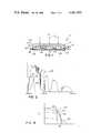
- the stacked solar cell module of the present inventionis shown generally at 10 in FIG. 1 in schematic representation.
- the stacked moduleis particularly significant in that a plurality of independent, solar cell panels each of which could be made separately operable are fabricated utilizing the desired materials responsive to predetermined different portions of the solar spectrum. By fabricating the panels separately, the particular techniques which are most proficient in the fabrication of the particular material may be utilized. After the completed fabrication of the solar cell panels, they are physically stacked one upon the other in a single module with an appropriate transparent interface there-between which functions to allow photons to pass there-through. In this manner, by tailoring the spectral response of the solar cell panels, they can be made responsive to different portions of the solar spectrum and effectively tailored to achieve maximum efficiency of collection with respect to those predetermined areas. As will be recognized, any number of such panels may be stacked one on top of the other in like manner in a single module and each panel may be constructed using any desired semiconductor material.
- this fabrication techniquepermits utilization of portions of the structure as the housing material for the completed stacked module.
- the stacked module 10includes a transparent substrate 12 which may be constructed of various materials such as glass or plastics, through which the photons of light illustrated at 14 pass.
- a solar cell panel 16constructed of thin film semiconductor material is deposited upon one surface of substrate 12 and is structured to provide an appropriate series of interconnected solar cells.
- the thin filmmay be, for example, a PIN microcrystalline thin film silicon/hydrogen solar cell layer having a first spectral response. Electrical connections or leads 18 and 20 are provided to collect the electrical energy generated through conversion of the photons 14 into electrical energy by the solar cell panel 16.
- a second substrate 22which may be metal, plastic or the like, which can withstand exposure to the elements and may form part of the ultimate housing, has positioned thereon typical single-crystal solar cells 24, 26 and 28 which may be separated from the substrate 22 by an appropriate layer 30 of insulating material or the like.
- Each of the solar cells 24 through 28may typically be constructed of single-crystal material in wafer form which has a PN junction formed therein for use as a solar cell as is well-known in the art and having a second and different spectral response.
- the cells 24, 26 and 28are inter-connected by appropriate electically conductive leads 32 and 34 to provide the usual series connected solar cells. Appropriate electrical leads 36, 38 then are connected to the series connection of solar cells and extend externally of the panel containing the cells 24, 26 and 28.
- top solar cell panelmay be fabricated using discrete cells with spaces therebetween. Obviously in such a case all of the light passing through the spaces will strike the panel or panels situated below the top panel.
- FIG. 2is a graph generally illustrating the response curves of the two stacked panels with respect to the solar spectrum.
- the solar spectrum 42extends from a frequency of approximately 350 nanometers to well beyond 2,500 nanometers.
- the monolithic thin film 16may be fabricated to have a spectral response as shown at 44 while the single-crystal solar cell module may be constructed to have a spectral response as shown at 46.
- FIG. 3is a typical voltage/current curve of a solar cell.
- the curve 48illustrates the current-voltage curve of the thin film layer 16 while the curve 50 represents the current-voltage curve of the single-crystal cell panel while the curve 52 represents the composite of the curves 48 and 50.
- the maximum power points of the three curvesare matched, thus providing substantially increased output from the stacked module as compared to either of the panels alone or from a typical single crystal panel without the thin film layer as shown at 51.
- the entire stacked solar cell module constructed in accordance with the present inventionis contained in a single package and can be substituted for the typical single-crystal solar cell panels currently being utilized in the field to form arrays positioned upon typical solar tracking devices and the like.
- the stacked solar cell module structure constructed in accordance with the present inventionallows a greater processing tolerance insofar as the fabrication of the single-crystal cells which form the single-crystal solar cell module.
- the depth of the PN junction in the typical single-crystal cellis relatively shallow so as to be more responsive to the shorter wavelength photons in the solar spectrum.
- the shorter wavelength solar energyis captured and converted by the monolithic layer 16 which is transparent to the longer wavelength solar energy.
- the longer wavesolar energypasses through the monolithic layer and the interface and strikes the standard single-crystal solar cells situated on the bottom of that module.
- microcrystalline thin film silicon/hydrogenSiH
- a-SiHamorphous silicon hydrogen
- a-SiNHamorphous silicon/nitrogen/hydrogen
- a-SiCHamorphous/silicon/carbon/hydrogen
- organic solar cellsuch as that taught in U.S. Pat. No. 4,127,738 or the like.
- cadmium tellurideCdTe
- GaAsgallium arsenide
- a-SiGeHamorphous silicon-germanium-hydrogen
- CuInSe 2copper indium selenide
- a-SiSnHamorphous silicon tin hydrogen
- the moduleswould be stacked with the appropriate interface material which is optically transparent, electrically insulative and thermally stable.
- materials which are effective to form the interface layerare air, inert gas such as argon, silicone, polyvinyl butyral (PVB), and ethylene vinyl acetate (EVA).
- TCtransparent conductive material
- the TC layermay be formed of any transparent conducting material known to the art and usable with respect to semi-conductors and having the appropriate optical, electrical and mechanical properties to be compatible with the semi-conductor material being utilized. For example, gold (Au), indium-tin-oxide (ITO), tin oxide (TO), or indium oxide (IO) or other similar materials well known to the art may be utilized.
- the voltages and optics of the systemmay be tailored in accordance with the particular semiconductor materials, compensational adjustments and cell doping being utilized.
- Another factor in using the particular TC layeris to choose a material which has a coefficient of thermal expansion and contraction which is compatible with the monolithic thin film. This will keep the film from being stressed during heating through absorption of the solar light.
- the appropriate index of refraction, extinction coefficient, thickness, conductivity and semi-conductor property of the TC layerone may select the effective filter characteristics of the TC layer; that is, to refract all or part of the solar spectrum or to permit it to pass through the TC layer.
- the TC layerwill be selected with properties such that the light falling on it will be allowed to pass uniformly into the layer below.
- the thin film solar cell panel used in accordance with the present inventionmay be constructed of various monolithic materials containing solar cells interconnected in various ways and deposited by various processing techniques.
- One preferred embodimentis illustrated in FIGS. 4-6, to which reference is hereby made. It should however be expressly understood that the following description and illustration is given by way of example only and not limitation.
- FIG. 4shows a monolithic thin film solar panel 60 constructed according to a preferred embodiment of the present invention.
- the paneldefines a plurality of elongated solar cells 62 connected electrically in series between a pair of external leads 64-64'.
- the cellsare shaped as narrow strips connected along opposite longitudinal edges to minimize series resistance losses. Connection between cells is accomplished directly through an unpatterned active film of the solar panel, without interrupting the film.
- Current generated by the cells in response to incident light (hv)travels a very short distance within each cell electrode before passing to the opposite electrode of an adjacent cell.
- the solar panel 60comprises a transparent substrate 66 such as that shown at 12 in FIG. 1, a transparent front electrode 68, a continuous thin film 70 of photovoltaic material and a patterned back electrode 72.
- the electrode 72comprises a plurality of back electrode portions 74 formed of a transparent conductive layer separated by a nonconducting spacing 76 and arranged to substantially overlie elongated photovoltaic regions of the thin film.
- the front electrode 68includes a transparent conductive layer 79 and a series of thickened contact portions or "stitch bars" 80.
- the layer 79is patterned to form a plurality of transparent electrode portions 82 separated by a spacing 84 and substantially underlying the respective photovoltaic regions.
- each front electrode portionpartially overlaps the back electrode portion of an adjacent photovoltaic region over a preselected area 86.
- a major feature of this constructionis the provision of conductive paths substantially transversely through the active thin film 70 between each front electrode portion and the back electrode portion of an adjacent photovoltaic region. Interconnection is accomplished at the area of electrode overlap to connect the photovoltaic regions electrically in series without patterning or otherwise interrupting the film.
- the stitch bars 80are tall enough and narrow enough, in comparison to the thin film 70, to electrically short through the film.
- the final configuration of the solar module 60is illustrated best in FIG. 6, wherein the stitch bars cause the subsequently applied film 70 to be distorted in a manner producing relatively thin regions 88 which are unable to withstand the cell voltage. Electrical conduction takes place through the regions 88. It is advantageous that the stitch bars be as rough as possible at their upper surfaces to focus the applied electric field and further reduce the resistance of the regions 88.
- the stitch bars 80are preferably approximately 25 microns thick, and the thin film 70 and the patterned transparent conductive layers 72 and 79 are approximately 2,000 and 1,000 angstroms thick, respectively.
- the film 70is sandwiched between a pair of conductive elements and the stitch bars 80 are at least two times thicker than the thickest portion of the film 70. This produces an effective short circuit through the film in the area of each stitch bar, but does not short out the cells 62 because the film 70 has a very high sheet resistance.
- the sheet resistancevirtually eliminates current within the plane of the film, leaving only substantially transverse currents developed within the photovoltaic regions and passed between the electrodes at the areas of overlap.
- the various layers and electrode portions of the panel 60are sequentially deposited on a major surface 90 of the substrate 66.
- the substrateis preferably glass or other suitable transparent material which is compatible with the materials of the stitch bars 80 and the transparent conductive layer 79.
- the stitch barsmay be applied to the substrate either before or after the transparent conductive layer, preferably by screen printing, electroplating or evaporation through a mask by techniques well known to the art.
- the material of the stitch barsmay be silver, aluminum or other material providing a high quality contact.
- the stitch bars 80are illustrated as grid lines or sections of grid lines passing through the preselected areas 86 of electrode overlap, it is not necessary that they be continuous or that they be lines at all. If the stitch bars are screen printed, they should be at least approximately 25 microns in height to operate satisfactorily. If evaporated, they should be at least 2 microns, and preferably 10 microns, in height. In each case, the aspect ratio (height divided by width) and the roughness of the stitch bars are the parameters responsible for the localized short circuit that permits the panel 60 to operate. If the width of the bars is substantial in relation to their height, or the bars are smooth rather than rough, it may be necessary to increase their height beyond the values set out above. The voltage and current characteristic of the cells may be tailored by spacing of the stitch bars.
- the transparent conductive layer 79is preferably a transparent conductive oxide (TCO), such as indium tin oxide (ITO), tin oxide (TO) or indium oxide (IO). If ITO or IO are used, they typically will be applied after the stitch bars 80, as illustrated in FIGS. 5 and 6, whereas a layer of TO would be applied directly upon the glass substrate (not shown).
- TCOtransparent conductive oxide
- ITOindium tin oxide
- TOtin oxide
- IOindium oxide
- the transparent conductive layer 79is preferably deposited, in the first instance, as a continuous layer.
- ITOfor example, may be deposited at approximately 300 degrees Celsius by vacuum evaporation of indium and tin in an oxygen atmosphere with glow discharge assistance. The glow discharge activates the oxygen to produce a high quality film.
- the transparent conductive layer 79is patterned using conventional techniques, such as laser scribing. In the case of the panel 60, the patterning operation entails removal of the transparent conductive layer along a series of parallel lines near the stitch bars 80, yielding the front electrode portions 82 separated by spacings 84. The front electrode portions are thus shaped as parallel strips corresponding generally in area to the cells 62 of FIG. 4.
- the front electrode portions 82 and the cells 62need not be shaped as strips, as long as each front electrode portion is provided with an interconnecting portion 92 which overlaps part of the back electrode portion of an adjacent photovoltaic region.
- the layer 79can be applied either before or after the stitch bars 80, it is preferably not patterned until after the stitch bars have been applied. The stitch bars 80 then act as a guide for patterning the layer 79.
- the thickness of the transparent conductive layer 79is selected to minimize reflection from the back surface of the layer and absorption of light by it. According to established optical principles, internal reflection losses within a transparent body are minimized when the thickness of the body is an odd multiple of the wavelength of incident light. For present purposes, the relevant wavelength is that at the peak of the spectral response of the photovoltaic material making up the film 70 as well as any solar cell layers therebelow.
- the panelmay be constructed of several layers of semiconductor material and each layer may be selectively doped to respond to a different band of spectral energy. Therefore, the TCO layer would be optically tailored to pass that band of energy.
- the TCO layerwill also be chosen to be thermally compatible with the layer 70.
- the thin film 70may contain any suitable photovoltaic material defining a photojunction for conversion of light to electrical energy.
- the film 70is microcrystalline thin film (MTF) silicon having N + , I and P + layers 94, 96 and 98, respectively, as illustrated in FIG. 5.
- MTFmicrocrystalline thin film
- the film 70is deposited by conventional glow discharge techniques without patterning or masking.
- the film 70extends continuously and completely across the stitch bars 80, the transparent conductive layer 79 and the spacings 84.
- the thickness of the film 70complete with all three layers of different conductivity types, is approximately 2,000 angstroms. Although this dimension depends upon the material of the film 70, the stitch bars 80 must, in any case, be tall and rough, as compared to the thickness of the thin film. Otherwise, the desired conductive paths through the film will not exist.
- the back electrode 72serves as the back contact of the cells 62 and it is preferably a TCO layer formed by following the same parameters as above described.
- the film 70Although shorting through the film 70 can be achieved in many circumstances with the structure described above, it is sometimes desirable to enhance localized conduction through the thin film 70 by applying heat to the solar panel 60.
- the stitch bars 80are relatively high, narrow and rough, such heat can cause diffusion of the back electrode material, and possibly the material of the stitch bars 80, into the semiconductive film 70.
- the resulting diffused regionis much more conductive than the bulk of the film and enhances interconnection of the cells.
- the conductive materialsmay diffuse into the film as discrete atoms or exist as particulates occupying interstitial sites within the film. In the latter case, the conductive regions of the film comprise mixtures of metallic and semiconductive particles.
- the lower panel of solar cells forming the stacked module of the present inventionmay be fabricated of various materials.
- a preferred embodimentuses single crystal silicon solar cells assembled into a panel as shown in FIGS. 7 and 8, to which reference is hereby made.
- a solar panel 110which includes an array of solar cells 112 positioned generally upon a back layer 120 and serially interconnected by the electrically conductive leads 114.
- a plurality of terminal arrangements 116are provided for establishing external electrical connection to the solar cells 112.
- the back layer 120comprises a metallic foil layer 130 laminated between a pair of electrically insulating and weatherable layers 132.
- a layer 136 of high dielectric strength materialmay be provided within the back layer 120 between the foil layer 130 and the inner weatherable layer 132.
- the layer 136thus enhances the electrical isolation of the foil layer 130 from the remainder of the solar panel 110, improving the high voltage chartacteristics of the panel.
- the layer 136is particularly useful for increasing the dielectric standoff between portions of the solar cells 112 and the foil layer 130.
- the solar cellsare commonly connected by a plurality of conductive ribbons 114 which can have burrs or other irregularities at cut ends thereof, approximating point sources of voltage relative to the foil layer. Without a layer of high dielectric strength such as the layer 132, a breakdown or excess current leakage might occur between the ribbons and the layer 130.
- the layer 136may comprise a layer of polyester or other suitable high dielectric material, preferably polyethylene terephthalate (PET).
- PETpolyethylene terephthalate
- This materialis available commercially as a high purity electronic grade film having a dielectric standoff of approximately 5,000 to 6,000 volts per mil and a resistivity of greater than 10 16 ohm-centimeters.
- a PET film at least 3 mils thickhas been found to be suitable for these purposes in panels rated at 250 volts.
- the array of solar cells 112is preferably encapsulated between a pair of transparent dielectric pottant layers 140 and 142.
- the pottant layers 140 and 142are preferably approximately 15 mils thick, and may be made of any suitable-transparent material, such as silicone, polyvinyl butyral (PVB) or ethylene vinyl acetate (EVA).
- PVBis a transparent thermoplastic pottant material which has been used in a number of prior solar panels.
- EVAis a thermosetting material which has also been used as an encapsulant.
- EVAEVA
- 10 parts of Dupont's Elvax-150 ethylene vinyl acetate formulationEVA
- 0.1 part of Ciba-Geigy's Tinuvin 770 and 0.3 part of American Cyanamid's Cyasorb UV-531 ultraviolet radiation absorbersEVA
- 0.2 part of Uniroyal's Naugard anti-oxidantEVA
- an organosilane primerfor example, 0.25 to 1.0 part of a mixture of 10% of Union Carbide's A1100 and 90% of Union Carbide's A174, or A174 alone, should improve the formulation's sticking characteristics during the panel formation process.
- the insulating and weatherable layers 132 of the back layer 120may comprise a suitable oriented film of polyvinyl fluoride resin, such as that manufactured by Dupont under the name Tedlar.
- the layers 136 and 132are preferably prelaminated to the foil layer 130 to form the back layer 120, permitting the back layer to be handled as a single element during the final manufacturing process.
- the panel 60is laminated together with the various portions comprising the panel 110 by application of appropriate heat and pressure.
- the TCO layer 72 of the panel 60is brought into contact with the pottant layer 142 which functions as the interface between the two panels of solar cells.
- appropriate heat and pressureis applied to the combination of elements for a period of time sufficient to securely adhere the panels together and to allow the layers 140 and 142 to fill the void present in the solar cell structures 116.
- the completed laminationis then placed within an appropriate frame which may be formed of any material desired, such as extruded aluminum.
- an appropriate framewhich may be formed of any material desired, such as extruded aluminum.
- FIGS. 9A, B, and CSome possible embodiments are shown in FIGS. 9A, B, and C, to which reference is hereby made.
- a pair of glass substrates 150 and 152may have formed on the surfaces thereof a thin film semiconductor panel as illustrated at 154 and 156.
- the two thin film semiconductor panelsmay then be brought together but separated by the optically transparent and electrically insulative layer 158 as above described.
- the thin film solar cell panels 154 and 156would be constructed of semiconductor material having different spectral responses.
- FIG. 9Bdiscloses glass substrates 160, 162 and 164.
- the glass substrate 160has a thin film solar cell panel 166 formed thereon while the substrates 162 and 164 have thin film panels 168 and 170 respectively formed thereon.
- An optically transparent and electrically insulative layer 172is used to bring the two panels 168 and 170 into face-to-face relationship much as is shown in FIG. 9A.
- An optically transparent layer 174is used to adhere the substrate 160 with its thin film solar cell panel 166 thereon to the substrate 162.
- the substrate 162is electrically insulative, greater freedom may be exercised in choosing the layer 174; however it will be recognized by those skilled in the art that the same layers as previously utilized, such as that at 172 may also be utilized in this embodiment.
- another embodimentincludes a substrate 176 which may be formed of glass and which has deposited thereon tandem layers 178 and 180 of a monolithic semiconductor material to provide the overall thin film solar cell panel 182.
- the layers 178 and 180may include active semiconductor material which has the same spectral response and is connected electrically together by a thin film tunneling layer 184 as described in the prior art.
- a layer of optically transparent and electrically insulative material 185is then used to secure the substrate 176 with its thin film solar cell panel 182 thereon to an additional solar cell panel 186 which may have any configuration desired such as a single crystal solar cell panel as shown in FIG. 1 or any combination of thin film solar cell panels as above described.
Landscapes
- Photovoltaic Devices (AREA)
Abstract
Description
Claims (24)
Priority Applications (1)
| Application Number | Priority Date | Filing Date | Title |
|---|---|---|---|
| US06/466,233US4461922A (en) | 1983-02-14 | 1983-02-14 | Solar cell module |
Applications Claiming Priority (1)
| Application Number | Priority Date | Filing Date | Title |
|---|---|---|---|
| US06/466,233US4461922A (en) | 1983-02-14 | 1983-02-14 | Solar cell module |
Publications (1)
| Publication Number | Publication Date |
|---|---|
| US4461922Atrue US4461922A (en) | 1984-07-24 |
Family
ID=23850993
Family Applications (1)
| Application Number | Title | Priority Date | Filing Date |
|---|---|---|---|
| US06/466,233Expired - LifetimeUS4461922A (en) | 1983-02-14 | 1983-02-14 | Solar cell module |
Country Status (1)
| Country | Link |
|---|---|
| US (1) | US4461922A (en) |
Cited By (195)
| Publication number | Priority date | Publication date | Assignee | Title |
|---|---|---|---|---|
| US4499658A (en)* | 1983-09-06 | 1985-02-19 | Atlantic Richfield Company | Solar cell laminates |
| US4513168A (en)* | 1984-04-19 | 1985-04-23 | Varian Associates, Inc. | Three-terminal solar cell circuit |
| US4625070A (en)* | 1985-08-30 | 1986-11-25 | Atlantic Richfield Company | Laminated thin film solar module |
| US4631352A (en)* | 1985-12-17 | 1986-12-23 | The United States Of America As Represented By The Administrator Of The National Aeronautics And Space Administration | High band gap II-VI and III-V tunneling junctions for silicon multijunction solar cells |
| US4638111A (en)* | 1985-06-04 | 1987-01-20 | Atlantic Richfield Company | Thin film solar cell module |
| US4658086A (en)* | 1985-06-03 | 1987-04-14 | Chevron Research Company | Photovoltaic cell package assembly for mechanically stacked photovoltaic cells |
| US4663495A (en)* | 1985-06-04 | 1987-05-05 | Atlantic Richfield Company | Transparent photovoltaic module |
| US4734379A (en)* | 1985-09-18 | 1988-03-29 | Fuji Electric Corporate Research And Development Ltd. | Method of manufacture of solar battery |
| US4914044A (en)* | 1987-08-20 | 1990-04-03 | Siemens Aktiengesellschaft | Method of making tandem solar cell module |
| US5078803A (en)* | 1989-09-22 | 1992-01-07 | Siemens Solar Industries L.P. | Solar cells incorporating transparent electrodes comprising hazy zinc oxide |
| WO1992000488A1 (en)* | 1990-06-22 | 1992-01-09 | Fabbian Franco & F.Lli S.N.C. | Support for light diffusers |
| US5261969A (en)* | 1992-04-14 | 1993-11-16 | The Boeing Company | Monolithic voltage-matched tandem photovoltaic cell and method for making same |
| US5352530A (en)* | 1985-12-23 | 1994-10-04 | Bridgestone Corporation | Transparent films and laminates having the same |
| US5998808A (en)* | 1997-06-27 | 1999-12-07 | Sony Corporation | Three-dimensional integrated circuit device and its manufacturing method |
| US6515217B1 (en) | 2001-09-11 | 2003-02-04 | Eric Aylaian | Solar cell having a three-dimensional array of photovoltaic cells enclosed within an enclosure having reflective surfaces |
| US20030047207A1 (en)* | 2001-09-11 | 2003-03-13 | Eric Aylaian | Solar cell having a three-dimensional array of photovoltaic cells enclosed within an enclosure having reflective surfaces |
| EP1263039A3 (en)* | 2001-05-30 | 2004-03-17 | Canon Kabushiki Kaisha | Housing for power converter, and for photovoltaic element module and power generator using the same |
| US20060138606A1 (en)* | 2000-12-20 | 2006-06-29 | Adrianus De Ruiter | Photovoltaic device forming a glazing |
| US20060207646A1 (en)* | 2003-07-07 | 2006-09-21 | Christine Terreau | Encapsulation of solar cells |
| US20060213548A1 (en)* | 2005-03-22 | 2006-09-28 | Applied Materials, Inc. | Scalable photovoltaic cell and solar panel manufacturing with improved wiring |
| US20060225776A1 (en)* | 2005-04-08 | 2006-10-12 | Portable Pipe Hangers, Inc. | Skylight solar panel assembly |
| EP1732140A1 (en)* | 2005-06-06 | 2006-12-13 | Alcan Technology & Management Ltd. | Felxible substrate with photovoltaic cells and its manufacturing method |
| US20070062576A1 (en)* | 2003-09-05 | 2007-03-22 | Michael Duerr | Tandem dye-sensitised solar cell and method of its production |
| US20070264488A1 (en)* | 2006-05-15 | 2007-11-15 | Stion Corporation | Method and structure for thin film photovoltaic materials using semiconductor materials |
| US20080078437A1 (en)* | 2006-10-02 | 2008-04-03 | Plextronics, Inc. | Solar farms having ultra-low cost opv modules |
| US20080092953A1 (en)* | 2006-05-15 | 2008-04-24 | Stion Corporation | Method and structure for thin film photovoltaic materials using bulk semiconductor materials |
| US20080149169A1 (en)* | 2006-12-22 | 2008-06-26 | Lumeta, Inc. | Photovoltaic module for roofs |
| US20080149168A1 (en)* | 2006-12-22 | 2008-06-26 | Dri Solar Corporation | Photovoltaic module for roofs |
| EP1959502A1 (en)* | 2007-02-14 | 2008-08-20 | Imphy Alloys | Photovoltaic module and modules for producing energy or light |
| US20080202585A1 (en)* | 2004-01-20 | 2008-08-28 | Ryohsuke Yamanaka | Dye-Sensitized Solar Cell Module |
| US20080210294A1 (en)* | 2006-10-09 | 2008-09-04 | Mehrdad Moslehi | Solar module structures and assembly methods for pyramidal three-dimensional thin-film solar cells |
| US20080264477A1 (en)* | 2006-10-09 | 2008-10-30 | Soltaix, Inc. | Methods for manufacturing three-dimensional thin-film solar cells |
| US20080289684A1 (en)* | 2006-10-09 | 2008-11-27 | Soltaix, Inc. | Pyramidal three-dimensional thin-film solar cells |
| US20080302415A1 (en)* | 2006-03-18 | 2008-12-11 | Solyndra, Inc. | Elongated photovoltaic cells in casings with a filling layer |
| US20090017605A1 (en)* | 2007-07-10 | 2009-01-15 | Stion Corporation | Methods for doping nanostructured materials and nanostructured thin films |
| US20090042320A1 (en)* | 2006-10-09 | 2009-02-12 | Solexel, Inc. | Methods for liquid transfer coating of three-dimensional substrates |
| US20090087939A1 (en)* | 2007-09-28 | 2009-04-02 | Stion Corporation | Column structure thin film material using metal oxide bearing semiconductor material for solar cell devices |
| US20090087370A1 (en)* | 2007-09-28 | 2009-04-02 | Stion Corporation | Method and material for purifying iron disilicide for photovoltaic application |
| US20090117718A1 (en)* | 2007-06-29 | 2009-05-07 | Stion Corporation | Methods for infusing one or more materials into nano-voids if nanoporous or nanostructured materials |
| US20090183763A1 (en)* | 2008-01-18 | 2009-07-23 | Tenksolar, Inc | Flat-Plate Photovoltaic Module |
| US20090183760A1 (en)* | 2008-01-18 | 2009-07-23 | Tenksolar Inc | Redundant electrical architecture for photovoltaic modules |
| US20090217980A1 (en)* | 2005-03-04 | 2009-09-03 | Heliatek Gmbh | Organic Photoactive Device |
| US20090301549A1 (en)* | 2006-10-09 | 2009-12-10 | Soltaix, Inc. | Solar module structures and assembly methods for three-dimensional thin-film solar cells |
| US20090301552A1 (en)* | 2008-06-06 | 2009-12-10 | Basf Se | Chlorinated naphthalenetetracarboxylic acid derivatives, preparation thereof and use thereof in organic electronics |
| DE102008034256A1 (en) | 2008-07-18 | 2010-01-21 | Technische Universität Dresden | Photoactive component with organic layers |
| DE102008036310A1 (en) | 2008-07-29 | 2010-02-11 | Technische Universität Dresden | Organic photoactive component, in particular organic solar cell or organic photodetector |
| US20100078056A1 (en)* | 2008-10-01 | 2010-04-01 | International Business Machines Corporation | Optical tandem photovoltaic cell panels |
| US20100116316A1 (en)* | 2008-11-26 | 2010-05-13 | Solexel, Inc. | Truncated pyramid structures for see-through solar cells |
| US20100131108A1 (en)* | 2008-01-18 | 2010-05-27 | Tenksolar, Inc | Thin-film photovoltaic module |
| US20100144080A1 (en)* | 2008-06-02 | 2010-06-10 | Solexel, Inc. | Method and apparatus to transfer coat uneven surface |
| US20100148319A1 (en)* | 2008-11-13 | 2010-06-17 | Solexel, Inc. | Substrates for High-Efficiency Thin-Film Solar Cells Based on Crystalline Templates |
| US20100170556A1 (en)* | 2009-01-06 | 2010-07-08 | Sunlight Photonics Inc. | Multi-junction pv module |
| US20100171108A1 (en)* | 2007-06-22 | 2010-07-08 | Basf Se | Use of n,n'-bis(1,1-dihydroperfluoro-c3-c5-alkyl)-perylene-3,4:9,10- tetracarboxylic diimides |
| US20100203711A1 (en)* | 2009-02-06 | 2010-08-12 | Solexel, Inc. | Trench Formation Method For Releasing A Thin-Film Substrate From A Reusable Semiconductor Template |
| WO2010097433A1 (en) | 2009-02-26 | 2010-09-02 | Basf Se | Quinone compounds as dopants in organic electronics |
| CN101840945A (en)* | 2009-03-21 | 2010-09-22 | 基奥托光电有限责任公司 | Photoelectric module |
| WO2010112452A1 (en) | 2009-03-30 | 2010-10-07 | Basf Se | Oligocondensed perylene bisimides |
| USD625695S1 (en) | 2008-10-14 | 2010-10-19 | Stion Corporation | Patterned thin film photovoltaic module |
| US20100267245A1 (en)* | 2009-04-14 | 2010-10-21 | Solexel, Inc. | High efficiency epitaxial chemical vapor deposition (cvd) reactor |
| US20100267186A1 (en)* | 2008-11-13 | 2010-10-21 | Solexel, Inc. | Method for fabricating a three-dimensional thin-film semiconductor substrate from a template |
| US20100279494A1 (en)* | 2006-10-09 | 2010-11-04 | Solexel, Inc. | Method For Releasing a Thin-Film Substrate |
| US20100282293A1 (en)* | 2009-01-21 | 2010-11-11 | Tenksolar | Illumination agnostic solar panel |
| USD627696S1 (en) | 2009-07-01 | 2010-11-23 | Stion Corporation | Pin striped thin film solar module for recreational vehicle |
| WO2010133205A1 (en) | 2009-05-18 | 2010-11-25 | Technische Universität Dresden | Organic solar cell or photodetector having improved absorption |
| US20100294328A1 (en)* | 2009-05-20 | 2010-11-25 | Jia-Ting Wan | Photovoltaic Generator |
| US20100294356A1 (en)* | 2009-04-24 | 2010-11-25 | Solexel, Inc. | Integrated 3-dimensional and planar metallization structure for thin film solar cells |
| USD628332S1 (en) | 2009-06-12 | 2010-11-30 | Stion Corporation | Pin striped thin film solar module for street lamp |
| US20100304521A1 (en)* | 2006-10-09 | 2010-12-02 | Solexel, Inc. | Shadow Mask Methods For Manufacturing Three-Dimensional Thin-Film Solar Cells |
| US20100300518A1 (en)* | 2009-05-29 | 2010-12-02 | Solexel, Inc. | Three-dimensional thin-film semiconductor substrate with through-holes and methods of manufacturing |
| US20100304522A1 (en)* | 2009-05-05 | 2010-12-02 | Solexel, Inc. | Ion implantation fabrication process for thin-film crystalline silicon solar cells |
| DE102009036110A1 (en) | 2009-06-05 | 2010-12-09 | Heliatek Gmbh | Light absorbing organic device |
| WO2010139310A2 (en) | 2009-06-05 | 2010-12-09 | Technische Universität Dresden | Inverted or transparent organic solar cell or photodetector having improved absorption |
| WO2011000939A1 (en) | 2009-07-03 | 2011-01-06 | Basf Se | Use of substituted periflanthenes in organic solar cells |
| WO2011004329A1 (en) | 2009-07-08 | 2011-01-13 | Total S.A. | Method for manufacturing photovoltaic cells with multiple junctions and multiple electrodes |
| US20110014742A1 (en)* | 2009-05-22 | 2011-01-20 | Solexel, Inc. | Method of creating reusable template for detachable thin film substrate |
| USD632415S1 (en) | 2009-06-13 | 2011-02-08 | Stion Corporation | Pin striped thin film solar module for cluster lamp |
| US20110030610A1 (en)* | 2009-05-05 | 2011-02-10 | Solexel, Inc. | High-productivity porous semiconductor manufacturing equipment |
| CN101976855A (en)* | 2010-11-28 | 2011-02-16 | 河海大学常州校区 | Intelligent solar cell component and control method of array thereof |
| US20110061711A1 (en)* | 2009-09-12 | 2011-03-17 | Yuhao Luo | Building-integrated solar photovoltaic panel |
| US7939454B1 (en) | 2008-05-31 | 2011-05-10 | Stion Corporation | Module and lamination process for multijunction cells |
| US20110124145A1 (en)* | 2006-10-09 | 2011-05-26 | Solexel, Inc. | Template for three-dimensional thin-film solar cell manufacturing and methods of use |
| US20110120882A1 (en)* | 2009-01-15 | 2011-05-26 | Solexel, Inc. | Porous silicon electro-etching system and method |
| US20110146765A1 (en)* | 2009-12-21 | 2011-06-23 | Junyong Ahn | Solar cell and method for manufacturing the same |
| US20110155222A1 (en)* | 2008-06-12 | 2011-06-30 | Bayer Materialscience Ag | Light, rigid, self-supporting solar module and method for the production thereof |
| US20110203649A1 (en)* | 2010-02-19 | 2011-08-25 | Basf Se | Use of indanthrene compounds in organic photovoltaics |
| US20110247677A1 (en)* | 2010-04-13 | 2011-10-13 | Eric Forsyth | Temperature-controlled Photovoltaic Matrix and Method of Use |
| US8058092B2 (en) | 2007-09-28 | 2011-11-15 | Stion Corporation | Method and material for processing iron disilicide for photovoltaic application |
| US8067263B2 (en) | 2008-09-30 | 2011-11-29 | Stion Corporation | Thermal management and method for large scale processing of CIS and/or CIGS based thin films overlying glass substrates |
| US8075723B1 (en) | 2008-03-03 | 2011-12-13 | Stion Corporation | Laser separation method for manufacture of unit cells for thin film photovoltaic materials |
| EP2400575A1 (en) | 2010-06-24 | 2011-12-28 | heliatek GmbH | Optoelectronic construction element with organic layers |
| USD652262S1 (en) | 2009-06-23 | 2012-01-17 | Stion Corporation | Pin striped thin film solar module for cooler |
| US8105437B2 (en) | 2007-11-14 | 2012-01-31 | Stion Corporation | Method and system for large scale manufacture of thin film photovoltaic devices using multi-chamber configuration |
| US8168463B2 (en) | 2008-10-17 | 2012-05-01 | Stion Corporation | Zinc oxide film method and structure for CIGS cell |
| US20120103390A1 (en)* | 2009-06-30 | 2012-05-03 | Lg Innotek Co., Ltd | Solar Cell Apparatus |
| US8193028B2 (en) | 2008-10-06 | 2012-06-05 | Stion Corporation | Sulfide species treatment of thin film photovoltaic cell and manufacturing method |
| US8193076B2 (en) | 2006-10-09 | 2012-06-05 | Solexel, Inc. | Method for releasing a thin semiconductor substrate from a reusable template |
| US8198122B2 (en) | 2008-09-29 | 2012-06-12 | Stion Corporation | Bulk chloride species treatment of thin film photovoltaic cell and manufacturing method |
| WO2012078517A1 (en) | 2010-12-06 | 2012-06-14 | Plextronics, Inc. | Inks for solar cell inverted structures |
| USD662040S1 (en) | 2009-06-12 | 2012-06-19 | Stion Corporation | Pin striped thin film solar module for garden lamp |
| USD662041S1 (en) | 2009-06-23 | 2012-06-19 | Stion Corporation | Pin striped thin film solar module for laptop personal computer |
| US8207008B1 (en) | 2008-08-01 | 2012-06-26 | Stion Corporation | Affixing method and solar decal device using a thin film photovoltaic |
| US20120180855A1 (en)* | 2011-01-19 | 2012-07-19 | Qualcomm Mems Technologies, Inc. | Photovoltaic devices and methods of forming the same |
| WO2012103190A1 (en)* | 2011-01-27 | 2012-08-02 | Corning Incorporated | Laminated pv module package |
| US8236597B1 (en) | 2008-09-29 | 2012-08-07 | Stion Corporation | Bulk metal species treatment of thin film photovoltaic cell and manufacturing method |
| US8241940B2 (en) | 2010-02-12 | 2012-08-14 | Solexel, Inc. | Double-sided reusable template for fabrication of semiconductor substrates for photovoltaic cell and microelectronics device manufacturing |
| US20120204939A1 (en)* | 2010-08-23 | 2012-08-16 | Stion Corporation | Structure and Method for High Efficiency CIS/CIGS-based Tandem Photovoltaic Module |
| US8258000B2 (en) | 2008-09-29 | 2012-09-04 | Stion Corporation | Bulk sodium species treatment of thin film photovoltaic cell and manufacturing method |
| US8263494B2 (en) | 2010-01-25 | 2012-09-11 | Stion Corporation | Method for improved patterning accuracy for thin film photovoltaic panels |
| US8287942B1 (en) | 2007-09-28 | 2012-10-16 | Stion Corporation | Method for manufacture of semiconductor bearing thin film material |
| US8344243B2 (en) | 2008-11-20 | 2013-01-01 | Stion Corporation | Method and structure for thin film photovoltaic cell using similar material junction |
| US8377736B2 (en) | 2008-10-02 | 2013-02-19 | Stion Corporation | System and method for transferring substrates in large scale processing of CIGS and/or CIS devices |
| US8383450B2 (en) | 2008-09-30 | 2013-02-26 | Stion Corporation | Large scale chemical bath system and method for cadmium sulfide processing of thin film photovoltaic materials |
| US8394662B1 (en) | 2008-09-29 | 2013-03-12 | Stion Corporation | Chloride species surface treatment of thin film photovoltaic cell and manufacturing method |
| US8398772B1 (en) | 2009-08-18 | 2013-03-19 | Stion Corporation | Method and structure for processing thin film PV cells with improved temperature uniformity |
| US8399331B2 (en) | 2007-10-06 | 2013-03-19 | Solexel | Laser processing for high-efficiency thin crystalline silicon solar cell fabrication |
| US8425739B1 (en) | 2008-09-30 | 2013-04-23 | Stion Corporation | In chamber sodium doping process and system for large scale cigs based thin film photovoltaic materials |
| US8435822B2 (en) | 2008-09-30 | 2013-05-07 | Stion Corporation | Patterning electrode materials free from berm structures for thin film photovoltaic cells |
| US8436445B2 (en) | 2011-08-15 | 2013-05-07 | Stion Corporation | Method of manufacture of sodium doped CIGS/CIGSS absorber layers for high efficiency photovoltaic devices |
| US8435826B1 (en) | 2008-10-06 | 2013-05-07 | Stion Corporation | Bulk sulfide species treatment of thin film photovoltaic cell and manufacturing method |
| US8440903B1 (en) | 2008-02-21 | 2013-05-14 | Stion Corporation | Method and structure for forming module using a powder coating and thermal treatment process |
| US8461061B2 (en) | 2010-07-23 | 2013-06-11 | Stion Corporation | Quartz boat method and apparatus for thin film thermal treatment |
| US8476104B1 (en) | 2008-09-29 | 2013-07-02 | Stion Corporation | Sodium species surface treatment of thin film photovoltaic cell and manufacturing method |
| US8501521B1 (en) | 2008-09-29 | 2013-08-06 | Stion Corporation | Copper species surface treatment of thin film photovoltaic cell and manufacturing method |
| US8507786B1 (en) | 2009-06-27 | 2013-08-13 | Stion Corporation | Manufacturing method for patterning CIGS/CIS solar cells |
| US8537554B1 (en)* | 2009-05-15 | 2013-09-17 | Energy Related Devices, Inc. | Structured relief dielectric heat sink for planar photovoltaic cells and semiconductor devices |
| US8617917B2 (en) | 2008-06-25 | 2013-12-31 | Stion Corporation | Consumable adhesive layer for thin film photovoltaic material |
| US8628997B2 (en) | 2010-10-01 | 2014-01-14 | Stion Corporation | Method and device for cadmium-free solar cells |
| US8642138B2 (en) | 2008-06-11 | 2014-02-04 | Stion Corporation | Processing method for cleaning sulfur entities of contact regions |
| US8673675B2 (en) | 2008-09-30 | 2014-03-18 | Stion Corporation | Humidity control and method for thin film photovoltaic materials |
| US8691618B2 (en) | 2008-09-29 | 2014-04-08 | Stion Corporation | Metal species surface treatment of thin film photovoltaic cell and manufacturing method |
| US8728200B1 (en) | 2011-01-14 | 2014-05-20 | Stion Corporation | Method and system for recycling processing gas for selenization of thin film photovoltaic materials |
| US8741689B2 (en) | 2008-10-01 | 2014-06-03 | Stion Corporation | Thermal pre-treatment process for soda lime glass substrate for thin film photovoltaic materials |
| US8759671B2 (en) | 2007-09-28 | 2014-06-24 | Stion Corporation | Thin film metal oxide bearing semiconductor material for single junction solar cell devices |
| US8772078B1 (en) | 2008-03-03 | 2014-07-08 | Stion Corporation | Method and system for laser separation for exclusion region of multi-junction photovoltaic materials |
| US20140224314A1 (en)* | 2011-04-14 | 2014-08-14 | Kenji Kido | Resin sheet for sealing solar cell, solar cell module using same, and method for manufacturing solar cell module |
| US8809096B1 (en) | 2009-10-22 | 2014-08-19 | Stion Corporation | Bell jar extraction tool method and apparatus for thin film photovoltaic materials |
| US8829330B2 (en) | 2010-02-23 | 2014-09-09 | Tenksolar, Inc. | Highly efficient solar arrays |
| US8829337B1 (en)* | 2005-11-06 | 2014-09-09 | Banpil Photonics, Inc. | Photovoltaic cells based on nano or micro-scale structures |
| US8828517B2 (en) | 2009-03-23 | 2014-09-09 | Solexel, Inc. | Structure and method for improving solar cell efficiency and mechanical strength |
| WO2014140850A2 (en) | 2013-03-11 | 2014-09-18 | Saudi Basic Industries Corporation | Aryloxy-phthalocyanines of group iv metals |
| WO2014140829A1 (en) | 2013-03-11 | 2014-09-18 | Saudi Basic Industries Corporation | Aryloxy-phthalocyanines of group iii metals |
| US8859880B2 (en) | 2010-01-22 | 2014-10-14 | Stion Corporation | Method and structure for tiling industrial thin-film solar devices |
| US8906218B2 (en) | 2010-05-05 | 2014-12-09 | Solexel, Inc. | Apparatus and methods for uniformly forming porous semiconductor on a substrate |
| US8941132B2 (en) | 2008-09-10 | 2015-01-27 | Stion Corporation | Application specific solar cell and method for manufacture using thin film photovoltaic materials |
| US8946547B2 (en) | 2010-08-05 | 2015-02-03 | Solexel, Inc. | Backplane reinforcement and interconnects for solar cells |
| US8962380B2 (en) | 2009-12-09 | 2015-02-24 | Solexel, Inc. | High-efficiency photovoltaic back-contact solar cell structures and manufacturing methods using thin planar semiconductor absorbers |
| WO2015036529A1 (en) | 2013-09-13 | 2015-03-19 | Heliatek Gmbh | Organic electronic device with active layer |
| US20150083186A1 (en)* | 2013-09-24 | 2015-03-26 | Kabushiki Kaisha Toshiba | Multi-junction solar cell |
| US8998606B2 (en) | 2011-01-14 | 2015-04-07 | Stion Corporation | Apparatus and method utilizing forced convection for uniform thermal treatment of thin film devices |
| US9076642B2 (en) | 2009-01-15 | 2015-07-07 | Solexel, Inc. | High-Throughput batch porous silicon manufacturing equipment design and processing methods |
| US9087943B2 (en) | 2008-06-25 | 2015-07-21 | Stion Corporation | High efficiency photovoltaic cell and manufacturing method free of metal disulfide barrier material |
| US9096930B2 (en) | 2010-03-29 | 2015-08-04 | Stion Corporation | Apparatus for manufacturing thin film photovoltaic devices |
| US20150239342A1 (en)* | 2014-02-27 | 2015-08-27 | Toyota Jidosha Kabushiki Kaisha | Solar battery mounting structure |
| US20150285532A1 (en)* | 2012-10-26 | 2015-10-08 | Kabushiki Kaisha Toyota Jidoshokki | Heat conversion member and heat conversion laminate |
| WO2016027217A1 (en) | 2014-08-18 | 2016-02-25 | Basf Se | Organic semiconductor composition comprising liquid medium |
| US9299861B2 (en) | 2010-06-15 | 2016-03-29 | Tenksolar, Inc. | Cell-to-grid redundandt photovoltaic system |
| US9318644B2 (en) | 2009-05-05 | 2016-04-19 | Solexel, Inc. | Ion implantation and annealing for thin film crystalline solar cells |
| WO2013082074A3 (en)* | 2011-11-30 | 2016-05-19 | Corsam Technologies Llc | Multi-junction photovoltaic modules incorporating ultra-thin flexible glass |
| WO2016083914A1 (en) | 2014-11-26 | 2016-06-02 | Basf Se | 4-oxoquinoline compounds |
| US9508886B2 (en) | 2007-10-06 | 2016-11-29 | Solexel, Inc. | Method for making a crystalline silicon solar cell substrate utilizing flat top laser beam |
| US9543460B2 (en) | 2010-03-05 | 2017-01-10 | Momentive Performance Materials Gmbh | Curable polyorganosiloxane composition for use as an encapsulant for a solar cell module |
| US9680044B2 (en) | 2008-10-01 | 2017-06-13 | International Business Machines Corporation | Tandem nanofilm photovoltaic cells joined by wafer bonding |
| US9748414B2 (en) | 2011-05-20 | 2017-08-29 | Arthur R. Zingher | Self-activated front surface bias for a solar cell |
| US9773933B2 (en) | 2010-02-23 | 2017-09-26 | Tenksolar, Inc. | Space and energy efficient photovoltaic array |
| US9870937B2 (en) | 2010-06-09 | 2018-01-16 | Ob Realty, Llc | High productivity deposition reactor comprising a gas flow chamber having a tapered gas flow space |
| US9917260B2 (en) | 2013-08-23 | 2018-03-13 | Basf Se | Compounds with terminal heteroarylcyanovinylene groups and their use in organic solar cells |
| US10186664B2 (en) | 2014-06-17 | 2019-01-22 | Basf Se | N-fluoroalkyl-substituted dibromonaphthalene diimides and their use as semiconductor |
| US10490682B2 (en) | 2018-03-14 | 2019-11-26 | National Mechanical Group Corp. | Frame-less encapsulated photo-voltaic solar panel supporting solar cell modules encapsulated within multiple layers of optically-transparent epoxy-resin materials |
| US10535785B2 (en) | 2014-12-19 | 2020-01-14 | Sunpower Corporation | Laser beam shaping for foil-based metallization of solar cells |
| US10566474B2 (en) | 2013-12-20 | 2020-02-18 | Sunpower Corporation | Single-step metal bond and contact formation for solar cells |
| US10593825B2 (en) | 2016-05-13 | 2020-03-17 | Sunpower Corporation | Roll-to-roll metallization of solar cells |
| US10615296B2 (en) | 2014-03-28 | 2020-04-07 | Sunpower Corporation | Foil-based metallization of solar cells |
| US10672924B2 (en) | 2015-10-29 | 2020-06-02 | Sunpower Corporation | Laser foil trim approaches for foil-based metallization for solar cells |
| US10700222B2 (en) | 2014-03-28 | 2020-06-30 | Sunpower Corporation | Metallization of solar cells |
| US10727369B2 (en) | 2016-09-30 | 2020-07-28 | Sunpower Corporation | Conductive foil based metallization of solar cells |
| US10741762B2 (en) | 2012-05-02 | 2020-08-11 | Clap Co., Ltd. | Method for the deposition of an organic material |
| US10879413B2 (en) | 2013-12-20 | 2020-12-29 | Sunpower Corporation | Contacts for solar cells |
| US10930804B2 (en) | 2013-09-27 | 2021-02-23 | Sunpower Corporation | Metallization of solar cells using metal foils |
| US10971638B2 (en) | 2016-07-01 | 2021-04-06 | Sunpower Corporation | Laser techniques for foil-based metallization of solar cells |
| US20210288114A1 (en)* | 2015-07-03 | 2021-09-16 | Samsung Electronics Co., Ltd. | Organic photoelectronic device and image sensor |
| US11205733B2 (en)* | 2019-07-11 | 2021-12-21 | Ricardo Garcia | Semi-transparent solar panel apparatus |
| US11276785B2 (en) | 2018-04-06 | 2022-03-15 | Sunpower Corporation | Laser assisted metallization process for solar cell fabrication |
| US11362234B2 (en) | 2018-04-06 | 2022-06-14 | Sunpower Corporation | Local patterning and metallization of semiconductor structures using a laser beam |
| US11362220B2 (en) | 2018-04-06 | 2022-06-14 | Sunpower Corporation | Local metallization for semiconductor substrates using a laser beam |
| US11424373B2 (en) | 2016-04-01 | 2022-08-23 | Sunpower Corporation | Thermocompression bonding approaches for foil-based metallization of non-metal surfaces of solar cells |
| US11431282B2 (en)* | 2017-09-28 | 2022-08-30 | Tesla, Inc. | Glass cover with optical-filtering coating for managing color of a solar roof tile |
| US11646387B2 (en) | 2018-04-06 | 2023-05-09 | Maxeon Solar Pte. Ltd. | Laser assisted metallization process for solar cell circuit formation |
| US11664472B2 (en) | 2018-04-06 | 2023-05-30 | Maxeon Solar Pte. Ltd. | Laser assisted metallization process for solar cell stringing |
| US11894472B2 (en) | 2015-06-26 | 2024-02-06 | Maxeon Solar Pte. Ltd. | Leave-in etch mask for foil-based metallization of solar cells |
| US11908958B2 (en) | 2016-12-30 | 2024-02-20 | Maxeon Solar Pte. Ltd. | Metallization structures for solar cells |
| US11955921B2 (en) | 2019-08-06 | 2024-04-09 | Tesla, Inc. | System and method for improving color appearance of solar roofs |
| US12009438B2 (en) | 2014-09-18 | 2024-06-11 | Maxeon Solar Pte. Ltd. | Foil trim approaches for foil-based metallization of solar cells |
| US12057803B2 (en) | 2021-06-16 | 2024-08-06 | Conti Innovation Center, Llc | Mechanically stacked solar transmissive cells or modules |
| US12080811B2 (en) | 2012-12-21 | 2024-09-03 | Maxeon Solar Pte. Ltd. | Metal-foil-assisted fabrication of thin-silicon solar cell |
| US12408469B1 (en) | 2025-01-03 | 2025-09-02 | Conti Innovation Center, Llc | Optimizing cadmium (Cd) alloy solar cells with sputtered copper-doped zinc telluride (ZnTe:Cu) back contacts in the presence of hydrogen |
Citations (7)
| Publication number | Priority date | Publication date | Assignee | Title |
|---|---|---|---|---|
| FR1129220A (en)* | 1955-07-25 | 1957-01-17 | High efficiency photovoltaic cells | |
| US2949498A (en)* | 1955-10-31 | 1960-08-16 | Texas Instruments Inc | Solar energy converter |
| US3376163A (en)* | 1961-08-11 | 1968-04-02 | Itek Corp | Photosensitive cell |
| US4094704A (en)* | 1977-05-11 | 1978-06-13 | Milnes Arthur G | Dual electrically insulated solar cells |
| US4295002A (en)* | 1980-06-23 | 1981-10-13 | International Business Machines Corporation | Heterojunction V-groove multijunction solar cell |
| US4338480A (en)* | 1980-12-29 | 1982-07-06 | Varian Associates, Inc. | Stacked multijunction photovoltaic converters |
| US4400577A (en)* | 1981-07-16 | 1983-08-23 | Spear Reginald G | Thin solar cells |
- 1983
- 1983-02-14USUS06/466,233patent/US4461922A/ennot_activeExpired - Lifetime
Patent Citations (7)
| Publication number | Priority date | Publication date | Assignee | Title |
|---|---|---|---|---|
| FR1129220A (en)* | 1955-07-25 | 1957-01-17 | High efficiency photovoltaic cells | |
| US2949498A (en)* | 1955-10-31 | 1960-08-16 | Texas Instruments Inc | Solar energy converter |
| US3376163A (en)* | 1961-08-11 | 1968-04-02 | Itek Corp | Photosensitive cell |
| US4094704A (en)* | 1977-05-11 | 1978-06-13 | Milnes Arthur G | Dual electrically insulated solar cells |
| US4295002A (en)* | 1980-06-23 | 1981-10-13 | International Business Machines Corporation | Heterojunction V-groove multijunction solar cell |
| US4338480A (en)* | 1980-12-29 | 1982-07-06 | Varian Associates, Inc. | Stacked multijunction photovoltaic converters |
| US4400577A (en)* | 1981-07-16 | 1983-08-23 | Spear Reginald G | Thin solar cells |
Cited By (325)
| Publication number | Priority date | Publication date | Assignee | Title |
|---|---|---|---|---|
| US4499658A (en)* | 1983-09-06 | 1985-02-19 | Atlantic Richfield Company | Solar cell laminates |
| US4513168A (en)* | 1984-04-19 | 1985-04-23 | Varian Associates, Inc. | Three-terminal solar cell circuit |
| US4658086A (en)* | 1985-06-03 | 1987-04-14 | Chevron Research Company | Photovoltaic cell package assembly for mechanically stacked photovoltaic cells |
| EP0204567A3 (en)* | 1985-06-04 | 1989-04-26 | Atlantic Richfield Company | Thin film solar module |
| US4638111A (en)* | 1985-06-04 | 1987-01-20 | Atlantic Richfield Company | Thin film solar cell module |
| US4663495A (en)* | 1985-06-04 | 1987-05-05 | Atlantic Richfield Company | Transparent photovoltaic module |
| EP0204562A3 (en)* | 1985-06-04 | 1989-05-03 | Siemens Solar Industries L.P. | Transparent photovoltaic module |
| US4625070A (en)* | 1985-08-30 | 1986-11-25 | Atlantic Richfield Company | Laminated thin film solar module |
| US4734379A (en)* | 1985-09-18 | 1988-03-29 | Fuji Electric Corporate Research And Development Ltd. | Method of manufacture of solar battery |
| EP0215482A3 (en)* | 1985-09-18 | 1989-05-31 | Fuji Electric Corporate Research And Development Ltd. | Solar battery and method of manufacture |
| US4631352A (en)* | 1985-12-17 | 1986-12-23 | The United States Of America As Represented By The Administrator Of The National Aeronautics And Space Administration | High band gap II-VI and III-V tunneling junctions for silicon multijunction solar cells |
| US5352530A (en)* | 1985-12-23 | 1994-10-04 | Bridgestone Corporation | Transparent films and laminates having the same |
| US4914044A (en)* | 1987-08-20 | 1990-04-03 | Siemens Aktiengesellschaft | Method of making tandem solar cell module |
| US5078803A (en)* | 1989-09-22 | 1992-01-07 | Siemens Solar Industries L.P. | Solar cells incorporating transparent electrodes comprising hazy zinc oxide |
| WO1992000488A1 (en)* | 1990-06-22 | 1992-01-09 | Fabbian Franco & F.Lli S.N.C. | Support for light diffusers |
| US5261969A (en)* | 1992-04-14 | 1993-11-16 | The Boeing Company | Monolithic voltage-matched tandem photovoltaic cell and method for making same |
| US5998808A (en)* | 1997-06-27 | 1999-12-07 | Sony Corporation | Three-dimensional integrated circuit device and its manufacturing method |
| US20060138606A1 (en)* | 2000-12-20 | 2006-06-29 | Adrianus De Ruiter | Photovoltaic device forming a glazing |
| US7439600B2 (en)* | 2000-12-20 | 2008-10-21 | Adrianus De Ruiter | Photovoltaic device forming a glazing |
| US20080178808A1 (en)* | 2000-12-20 | 2008-07-31 | Energy Systems International Bv | Photovoltaic device forming a glazing |
| EP1263039A3 (en)* | 2001-05-30 | 2004-03-17 | Canon Kabushiki Kaisha | Housing for power converter, and for photovoltaic element module and power generator using the same |
| US6791024B2 (en) | 2001-05-30 | 2004-09-14 | Canon Kabushiki Kaisha | Power converter, and photovoltaic element module and power generator using the same |
| US7208674B2 (en) | 2001-09-11 | 2007-04-24 | Eric Aylaian | Solar cell having photovoltaic cells inclined at acute angle to each other |
| US20030047207A1 (en)* | 2001-09-11 | 2003-03-13 | Eric Aylaian | Solar cell having a three-dimensional array of photovoltaic cells enclosed within an enclosure having reflective surfaces |
| US20040084077A1 (en)* | 2001-09-11 | 2004-05-06 | Eric Aylaian | Solar collector having an array of photovoltaic cells oriented to receive reflected light |
| US6515217B1 (en) | 2001-09-11 | 2003-02-04 | Eric Aylaian | Solar cell having a three-dimensional array of photovoltaic cells enclosed within an enclosure having reflective surfaces |
| US20060207646A1 (en)* | 2003-07-07 | 2006-09-21 | Christine Terreau | Encapsulation of solar cells |
| US8847064B2 (en) | 2003-07-07 | 2014-09-30 | Dow Corning Corporation | Encapsulation of solar cells |
| US8847063B2 (en) | 2003-07-07 | 2014-09-30 | Dow Corning Corporation | Encapsulation of solar cells |
| US20070062576A1 (en)* | 2003-09-05 | 2007-03-22 | Michael Duerr | Tandem dye-sensitised solar cell and method of its production |
| US8237046B2 (en)* | 2004-01-20 | 2012-08-07 | Sharp Kabushiki Kaisha | Dye-sensitized solar cell module |
| US20080202585A1 (en)* | 2004-01-20 | 2008-08-28 | Ryohsuke Yamanaka | Dye-Sensitized Solar Cell Module |
| US8426727B2 (en) | 2005-03-04 | 2013-04-23 | Heliatek Gmbh | Organic photoactive device |
| DE202006021034U1 (en) | 2005-03-04 | 2011-12-28 | Heliatek Gmbh | Organic photoactive component |
| US20090217980A1 (en)* | 2005-03-04 | 2009-09-03 | Heliatek Gmbh | Organic Photoactive Device |
| US20060213548A1 (en)* | 2005-03-22 | 2006-09-28 | Applied Materials, Inc. | Scalable photovoltaic cell and solar panel manufacturing with improved wiring |
| US7759158B2 (en)* | 2005-03-22 | 2010-07-20 | Applied Materials, Inc. | Scalable photovoltaic cell and solar panel manufacturing with improved wiring |
| US20060225776A1 (en)* | 2005-04-08 | 2006-10-12 | Portable Pipe Hangers, Inc. | Skylight solar panel assembly |
| EP1732140A1 (en)* | 2005-06-06 | 2006-12-13 | Alcan Technology & Management Ltd. | Felxible substrate with photovoltaic cells and its manufacturing method |
| US8829337B1 (en)* | 2005-11-06 | 2014-09-09 | Banpil Photonics, Inc. | Photovoltaic cells based on nano or micro-scale structures |
| US20080302415A1 (en)* | 2006-03-18 | 2008-12-11 | Solyndra, Inc. | Elongated photovoltaic cells in casings with a filling layer |
| US8742252B2 (en)* | 2006-03-18 | 2014-06-03 | Solyndra, Llc | Elongated photovoltaic cells in casings with a filling layer |
| US20090007963A1 (en)* | 2006-03-18 | 2009-01-08 | Solyndra, Inc. | Elongated photovoltaic cells in casings with a filling layer |
| US20110000534A1 (en)* | 2006-03-18 | 2011-01-06 | Solyndra, Inc. | Elongated photovoltaic cells in casings with a filling layer |
| US8017860B2 (en) | 2006-05-15 | 2011-09-13 | Stion Corporation | Method and structure for thin film photovoltaic materials using bulk semiconductor materials |
| US20070264488A1 (en)* | 2006-05-15 | 2007-11-15 | Stion Corporation | Method and structure for thin film photovoltaic materials using semiconductor materials |
| US20080092953A1 (en)* | 2006-05-15 | 2008-04-24 | Stion Corporation | Method and structure for thin film photovoltaic materials using bulk semiconductor materials |
| US9105776B2 (en) | 2006-05-15 | 2015-08-11 | Stion Corporation | Method and structure for thin film photovoltaic materials using semiconductor materials |
| US8314326B2 (en) | 2006-05-15 | 2012-11-20 | Stion Corporation | Method and structure for thin film photovoltaic materials using bulk semiconductor materials |
| US20080078437A1 (en)* | 2006-10-02 | 2008-04-03 | Plextronics, Inc. | Solar farms having ultra-low cost opv modules |
| US20090042320A1 (en)* | 2006-10-09 | 2009-02-12 | Solexel, Inc. | Methods for liquid transfer coating of three-dimensional substrates |
| US8035027B2 (en)* | 2006-10-09 | 2011-10-11 | Solexel, Inc. | Solar module structures and assembly methods for pyramidal three-dimensional thin-film solar cells |
| US20100304521A1 (en)* | 2006-10-09 | 2010-12-02 | Solexel, Inc. | Shadow Mask Methods For Manufacturing Three-Dimensional Thin-Film Solar Cells |
| US8293558B2 (en) | 2006-10-09 | 2012-10-23 | Solexel, Inc. | Method for releasing a thin-film substrate |
| US20080210294A1 (en)* | 2006-10-09 | 2008-09-04 | Mehrdad Moslehi | Solar module structures and assembly methods for pyramidal three-dimensional thin-film solar cells |
| US9349887B2 (en) | 2006-10-09 | 2016-05-24 | Solexel, Inc. | Three-dimensional thin-film solar cells |
| US20090301549A1 (en)* | 2006-10-09 | 2009-12-10 | Soltaix, Inc. | Solar module structures and assembly methods for three-dimensional thin-film solar cells |
| US9397250B2 (en) | 2006-10-09 | 2016-07-19 | Solexel, Inc. | Releasing apparatus for separating a semiconductor substrate from a semiconductor template |
| US20090107545A1 (en)* | 2006-10-09 | 2009-04-30 | Soltaix, Inc. | Template for pyramidal three-dimensional thin-film solar cell manufacturing and methods of use |
| US20100279494A1 (en)* | 2006-10-09 | 2010-11-04 | Solexel, Inc. | Method For Releasing a Thin-Film Substrate |
| US8193076B2 (en) | 2006-10-09 | 2012-06-05 | Solexel, Inc. | Method for releasing a thin semiconductor substrate from a reusable template |
| US8512581B2 (en) | 2006-10-09 | 2013-08-20 | Solexel, Inc. | Methods for liquid transfer coating of three-dimensional substrates |
| US20080264477A1 (en)* | 2006-10-09 | 2008-10-30 | Soltaix, Inc. | Methods for manufacturing three-dimensional thin-film solar cells |
| US20080289684A1 (en)* | 2006-10-09 | 2008-11-27 | Soltaix, Inc. | Pyramidal three-dimensional thin-film solar cells |
| US20110124145A1 (en)* | 2006-10-09 | 2011-05-26 | Solexel, Inc. | Template for three-dimensional thin-film solar cell manufacturing and methods of use |
| US7999174B2 (en) | 2006-10-09 | 2011-08-16 | Solexel, Inc. | Solar module structures and assembly methods for three-dimensional thin-film solar cells |
| US8035028B2 (en) | 2006-10-09 | 2011-10-11 | Solexel, Inc. | Pyramidal three-dimensional thin-film solar cells |
| US11205991B2 (en) | 2006-12-22 | 2021-12-21 | Lumeta Holdings, Llc | Photovoltaic module for roofs |
| US7531740B2 (en) | 2006-12-22 | 2009-05-12 | Lumeta, Inc. | Photovoltaic module for roofs |
| US7557291B2 (en) | 2006-12-22 | 2009-07-07 | Lumeta, Inc. | Photovoltaic module for roofs |
| US20080149169A1 (en)* | 2006-12-22 | 2008-06-26 | Lumeta, Inc. | Photovoltaic module for roofs |
| US20080149168A1 (en)* | 2006-12-22 | 2008-06-26 | Dri Solar Corporation | Photovoltaic module for roofs |
| US20090205704A1 (en)* | 2006-12-22 | 2009-08-20 | Lumeta, Inc. | Photovoltaic module for roofs |
| EP1959502A1 (en)* | 2007-02-14 | 2008-08-20 | Imphy Alloys | Photovoltaic module and modules for producing energy or light |
| WO2008125746A1 (en)* | 2007-02-14 | 2008-10-23 | Arcelormittal-Stainless & Nickel Alloys | Photovoltaic module and energy or light production modules |
| US20100089438A1 (en)* | 2007-02-14 | 2010-04-15 | Arcelormittal-Stainless & Nickel Alloys | Photovoltaic module and energy or light production modules |
| US20100171108A1 (en)* | 2007-06-22 | 2010-07-08 | Basf Se | Use of n,n'-bis(1,1-dihydroperfluoro-c3-c5-alkyl)-perylene-3,4:9,10- tetracarboxylic diimides |
| US8871305B2 (en) | 2007-06-29 | 2014-10-28 | Stion Corporation | Methods for infusing one or more materials into nano-voids of nanoporous or nanostructured materials |
| US20090117718A1 (en)* | 2007-06-29 | 2009-05-07 | Stion Corporation | Methods for infusing one or more materials into nano-voids if nanoporous or nanostructured materials |
| US8071179B2 (en) | 2007-06-29 | 2011-12-06 | Stion Corporation | Methods for infusing one or more materials into nano-voids if nanoporous or nanostructured materials |
| US7919400B2 (en) | 2007-07-10 | 2011-04-05 | Stion Corporation | Methods for doping nanostructured materials and nanostructured thin films |
| US20090017605A1 (en)* | 2007-07-10 | 2009-01-15 | Stion Corporation | Methods for doping nanostructured materials and nanostructured thin films |
| US20100154998A1 (en)* | 2007-08-17 | 2010-06-24 | Solexel, Inc. | Alternate use for low viscosity liquids and method to gel liquid |
| US8759671B2 (en) | 2007-09-28 | 2014-06-24 | Stion Corporation | Thin film metal oxide bearing semiconductor material for single junction solar cell devices |
| US20090087939A1 (en)* | 2007-09-28 | 2009-04-02 | Stion Corporation | Column structure thin film material using metal oxide bearing semiconductor material for solar cell devices |
| US20090087370A1 (en)* | 2007-09-28 | 2009-04-02 | Stion Corporation | Method and material for purifying iron disilicide for photovoltaic application |
| US8287942B1 (en) | 2007-09-28 | 2012-10-16 | Stion Corporation | Method for manufacture of semiconductor bearing thin film material |
| US8614396B2 (en) | 2007-09-28 | 2013-12-24 | Stion Corporation | Method and material for purifying iron disilicide for photovoltaic application |
| US8058092B2 (en) | 2007-09-28 | 2011-11-15 | Stion Corporation | Method and material for processing iron disilicide for photovoltaic application |
| US9508886B2 (en) | 2007-10-06 | 2016-11-29 | Solexel, Inc. | Method for making a crystalline silicon solar cell substrate utilizing flat top laser beam |
| US8399331B2 (en) | 2007-10-06 | 2013-03-19 | Solexel | Laser processing for high-efficiency thin crystalline silicon solar cell fabrication |
| US8512528B2 (en) | 2007-11-14 | 2013-08-20 | Stion Corporation | Method and system for large scale manufacture of thin film photovoltaic devices using single-chamber configuration |
| US8105437B2 (en) | 2007-11-14 | 2012-01-31 | Stion Corporation | Method and system for large scale manufacture of thin film photovoltaic devices using multi-chamber configuration |
| US8623677B2 (en) | 2007-11-14 | 2014-01-07 | Stion Corporation | Method and system for large scale manufacture of thin film photovoltaic devices using multi-chamber configuration |
| US8501507B2 (en) | 2007-11-14 | 2013-08-06 | Stion Corporation | Method for large scale manufacture of thin film photovoltaic devices using multi-chamber configuration |
| US8183066B2 (en) | 2007-11-14 | 2012-05-22 | Stion Corporation | Method and system for large scale manufacture of thin film photovoltaic devices using multi-chamber configuration |
| US8642361B2 (en) | 2007-11-14 | 2014-02-04 | Stion Corporation | Method and system for large scale manufacture of thin film photovoltaic devices using multi-chamber configuration |
| US8178370B2 (en) | 2007-11-14 | 2012-05-15 | Stion Corporation | Method and system for large scale manufacture of thin film photovoltaic devices using multi-chamber configuration |
| US20090183763A1 (en)* | 2008-01-18 | 2009-07-23 | Tenksolar, Inc | Flat-Plate Photovoltaic Module |
| US20100131108A1 (en)* | 2008-01-18 | 2010-05-27 | Tenksolar, Inc | Thin-film photovoltaic module |
| US8748727B2 (en)* | 2008-01-18 | 2014-06-10 | Tenksolar, Inc. | Flat-plate photovoltaic module |
| US8212139B2 (en)* | 2008-01-18 | 2012-07-03 | Tenksolar, Inc. | Thin-film photovoltaic module |
| US9768725B2 (en) | 2008-01-18 | 2017-09-19 | Tenksolar, Inc. | Redundant electrical architecture for photovoltaic modules |
| US20090183760A1 (en)* | 2008-01-18 | 2009-07-23 | Tenksolar Inc | Redundant electrical architecture for photovoltaic modules |
| US8933320B2 (en) | 2008-01-18 | 2015-01-13 | Tenksolar, Inc. | Redundant electrical architecture for photovoltaic modules |
| US8828778B2 (en) | 2008-01-18 | 2014-09-09 | Tenksolar, Inc. | Thin-film photovoltaic module |
| US8440903B1 (en) | 2008-02-21 | 2013-05-14 | Stion Corporation | Method and structure for forming module using a powder coating and thermal treatment process |
| US8075723B1 (en) | 2008-03-03 | 2011-12-13 | Stion Corporation | Laser separation method for manufacture of unit cells for thin film photovoltaic materials |
| US8772078B1 (en) | 2008-03-03 | 2014-07-08 | Stion Corporation | Method and system for laser separation for exclusion region of multi-junction photovoltaic materials |
| US7939454B1 (en) | 2008-05-31 | 2011-05-10 | Stion Corporation | Module and lamination process for multijunction cells |
| US20100144080A1 (en)* | 2008-06-02 | 2010-06-10 | Solexel, Inc. | Method and apparatus to transfer coat uneven surface |
| US20090301552A1 (en)* | 2008-06-06 | 2009-12-10 | Basf Se | Chlorinated naphthalenetetracarboxylic acid derivatives, preparation thereof and use thereof in organic electronics |
| US10214525B2 (en) | 2008-06-06 | 2019-02-26 | Basf Se | Chlorinated napthalenetetracarboxylic acid derivatives, preparation thereof and use thereof in organic electronics |
| WO2009147237A1 (en) | 2008-06-06 | 2009-12-10 | Basf Se | Chlorinated naphthalenetetracarboxylic acid derivatives, preparation thereof and use thereof in organic electronics |
| US9512354B2 (en) | 2008-06-06 | 2016-12-06 | Basf Se | Chlorinated naphthalenetetracarboxylic acid derivatives, preparation thereof and use thereof in organic electronics |
| US8642138B2 (en) | 2008-06-11 | 2014-02-04 | Stion Corporation | Processing method for cleaning sulfur entities of contact regions |
| US20110155222A1 (en)* | 2008-06-12 | 2011-06-30 | Bayer Materialscience Ag | Light, rigid, self-supporting solar module and method for the production thereof |
| US8617917B2 (en) | 2008-06-25 | 2013-12-31 | Stion Corporation | Consumable adhesive layer for thin film photovoltaic material |
| US9087943B2 (en) | 2008-06-25 | 2015-07-21 | Stion Corporation | High efficiency photovoltaic cell and manufacturing method free of metal disulfide barrier material |
| DE102008034256A1 (en) | 2008-07-18 | 2010-01-21 | Technische Universität Dresden | Photoactive component with organic layers |
| DE102008036310A1 (en) | 2008-07-29 | 2010-02-11 | Technische Universität Dresden | Organic photoactive component, in particular organic solar cell or organic photodetector |
| US8207008B1 (en) | 2008-08-01 | 2012-06-26 | Stion Corporation | Affixing method and solar decal device using a thin film photovoltaic |
| US8941132B2 (en) | 2008-09-10 | 2015-01-27 | Stion Corporation | Application specific solar cell and method for manufacture using thin film photovoltaic materials |
| US8476104B1 (en) | 2008-09-29 | 2013-07-02 | Stion Corporation | Sodium species surface treatment of thin film photovoltaic cell and manufacturing method |
| US8258000B2 (en) | 2008-09-29 | 2012-09-04 | Stion Corporation | Bulk sodium species treatment of thin film photovoltaic cell and manufacturing method |
| US8394662B1 (en) | 2008-09-29 | 2013-03-12 | Stion Corporation | Chloride species surface treatment of thin film photovoltaic cell and manufacturing method |
| US8691618B2 (en) | 2008-09-29 | 2014-04-08 | Stion Corporation | Metal species surface treatment of thin film photovoltaic cell and manufacturing method |
| US8236597B1 (en) | 2008-09-29 | 2012-08-07 | Stion Corporation | Bulk metal species treatment of thin film photovoltaic cell and manufacturing method |
| US8198122B2 (en) | 2008-09-29 | 2012-06-12 | Stion Corporation | Bulk chloride species treatment of thin film photovoltaic cell and manufacturing method |
| US8501521B1 (en) | 2008-09-29 | 2013-08-06 | Stion Corporation | Copper species surface treatment of thin film photovoltaic cell and manufacturing method |
| US8383450B2 (en) | 2008-09-30 | 2013-02-26 | Stion Corporation | Large scale chemical bath system and method for cadmium sulfide processing of thin film photovoltaic materials |
| US8084291B2 (en) | 2008-09-30 | 2011-12-27 | Stion Corporation | Thermal management and method for large scale processing of CIS and/or CIGS based thin films overlying glass substrates |
| US8088640B2 (en) | 2008-09-30 | 2012-01-03 | Stion Corporation | Thermal management and method for large scale processing of CIS and/or CIGS based thin films overlying glass substrates |
| US8076176B2 (en) | 2008-09-30 | 2011-12-13 | Stion Corporation | Thermal management and method for large scale processing of CIS and/or CIGS based thin films overlying glass substrates |
| US8071421B2 (en) | 2008-09-30 | 2011-12-06 | Stion Corporation | Thermal management and method for large scale processing of CIS and/or CIGS based thin films overlying glass substrates |
| US8067263B2 (en) | 2008-09-30 | 2011-11-29 | Stion Corporation | Thermal management and method for large scale processing of CIS and/or CIGS based thin films overlying glass substrates |
| US8425739B1 (en) | 2008-09-30 | 2013-04-23 | Stion Corporation | In chamber sodium doping process and system for large scale cigs based thin film photovoltaic materials |
| US8435822B2 (en) | 2008-09-30 | 2013-05-07 | Stion Corporation | Patterning electrode materials free from berm structures for thin film photovoltaic cells |
| US8318531B2 (en) | 2008-09-30 | 2012-11-27 | Stion Corporation | Thermal management and method for large scale processing of CIS and/or CIGS based thin films overlying glass substrates |
| US8673675B2 (en) | 2008-09-30 | 2014-03-18 | Stion Corporation | Humidity control and method for thin film photovoltaic materials |
| US8084292B2 (en) | 2008-09-30 | 2011-12-27 | Stion Corporation | Thermal management and method for large scale processing of CIS and/or CIGS based thin films overlying glass substrates |
| US9882076B2 (en) | 2008-10-01 | 2018-01-30 | International Businss Machines Corporation | Optical tandem photovoltaic cell panels |
| US20100078056A1 (en)* | 2008-10-01 | 2010-04-01 | International Business Machines Corporation | Optical tandem photovoltaic cell panels |
| US9837571B2 (en) | 2008-10-01 | 2017-12-05 | International Business Machines Corporation | Tandem nanofilm photovoltaic cells joined by wafer bonding |
| US9680044B2 (en) | 2008-10-01 | 2017-06-13 | International Business Machines Corporation | Tandem nanofilm photovoltaic cells joined by wafer bonding |
| US8138410B2 (en) | 2008-10-01 | 2012-03-20 | International Business Machines Corporation | Optical tandem photovoltaic cell panels |
| US8741689B2 (en) | 2008-10-01 | 2014-06-03 | Stion Corporation | Thermal pre-treatment process for soda lime glass substrate for thin film photovoltaic materials |
| US8377736B2 (en) | 2008-10-02 | 2013-02-19 | Stion Corporation | System and method for transferring substrates in large scale processing of CIGS and/or CIS devices |
| US8193028B2 (en) | 2008-10-06 | 2012-06-05 | Stion Corporation | Sulfide species treatment of thin film photovoltaic cell and manufacturing method |
| US8435826B1 (en) | 2008-10-06 | 2013-05-07 | Stion Corporation | Bulk sulfide species treatment of thin film photovoltaic cell and manufacturing method |
| USD625695S1 (en) | 2008-10-14 | 2010-10-19 | Stion Corporation | Patterned thin film photovoltaic module |
| US8557625B1 (en) | 2008-10-17 | 2013-10-15 | Stion Corporation | Zinc oxide film method and structure for cigs cell |
| US8168463B2 (en) | 2008-10-17 | 2012-05-01 | Stion Corporation | Zinc oxide film method and structure for CIGS cell |
| US8664737B2 (en) | 2008-11-13 | 2014-03-04 | Selexel, Inc. | Three-dimensional semiconductor template for making high efficiency thin-film solar cells |
| US20100175752A1 (en)* | 2008-11-13 | 2010-07-15 | Solexel, Inc. | High-Efficiency Thin-Film Solar Cells |
| US20100148318A1 (en)* | 2008-11-13 | 2010-06-17 | Solexel, Inc. | Three-Dimensional Semiconductor Template for Making High Efficiency Thin-Film Solar Cells |
| US20100148319A1 (en)* | 2008-11-13 | 2010-06-17 | Solexel, Inc. | Substrates for High-Efficiency Thin-Film Solar Cells Based on Crystalline Templates |
| US8288195B2 (en) | 2008-11-13 | 2012-10-16 | Solexel, Inc. | Method for fabricating a three-dimensional thin-film semiconductor substrate from a template |
| US8294026B2 (en) | 2008-11-13 | 2012-10-23 | Solexel, Inc. | High-efficiency thin-film solar cells |
| US20100267186A1 (en)* | 2008-11-13 | 2010-10-21 | Solexel, Inc. | Method for fabricating a three-dimensional thin-film semiconductor substrate from a template |
| US8168465B2 (en) | 2008-11-13 | 2012-05-01 | Solexel, Inc. | Three-dimensional semiconductor template for making high efficiency thin-film solar cells |
| US8344243B2 (en) | 2008-11-20 | 2013-01-01 | Stion Corporation | Method and structure for thin film photovoltaic cell using similar material junction |
| US8053665B2 (en) | 2008-11-26 | 2011-11-08 | Solexel, Inc. | Truncated pyramid structures for see-through solar cells |
| US20100116316A1 (en)* | 2008-11-26 | 2010-05-13 | Solexel, Inc. | Truncated pyramid structures for see-through solar cells |
| US20100170556A1 (en)* | 2009-01-06 | 2010-07-08 | Sunlight Photonics Inc. | Multi-junction pv module |
| EP2386122A4 (en)* | 2009-01-06 | 2013-02-20 | Sunlight Photonics Inc | PHOTOVOLTAIC MODULE WITH MULTIPLE JUNCTION |
| US8835748B2 (en) | 2009-01-06 | 2014-09-16 | Sunlight Photonics Inc. | Multi-junction PV module |
| US9087948B1 (en) | 2009-01-06 | 2015-07-21 | Sunlight Photonics Inc. | Manufacturing method of multi-junction PV modules |
| WO2010080672A2 (en) | 2009-01-06 | 2010-07-15 | Sunlight Photonics Inc. | Multi-junction pv module |
| US10829864B2 (en) | 2009-01-15 | 2020-11-10 | Trutag Technologies, Inc. | Apparatus and methods for uniformly forming porous semiconductor on a substrate |
| US9076642B2 (en) | 2009-01-15 | 2015-07-07 | Solexel, Inc. | High-Throughput batch porous silicon manufacturing equipment design and processing methods |
| US20110120882A1 (en)* | 2009-01-15 | 2011-05-26 | Solexel, Inc. | Porous silicon electro-etching system and method |
| US8926803B2 (en) | 2009-01-15 | 2015-01-06 | Solexel, Inc. | Porous silicon electro-etching system and method |
| US8563847B2 (en) | 2009-01-21 | 2013-10-22 | Tenksolar, Inc | Illumination agnostic solar panel |
| US20100282293A1 (en)* | 2009-01-21 | 2010-11-11 | Tenksolar | Illumination agnostic solar panel |
| US9543890B2 (en) | 2009-01-21 | 2017-01-10 | Tenksolar, Inc. | Illumination agnostic solar panel |
| US20100203711A1 (en)* | 2009-02-06 | 2010-08-12 | Solexel, Inc. | Trench Formation Method For Releasing A Thin-Film Substrate From A Reusable Semiconductor Template |
| US8278192B2 (en) | 2009-02-06 | 2012-10-02 | Solexel | Trench formation method for releasing a thin-film substrate from a reusable semiconductor template |
| WO2010097433A1 (en) | 2009-02-26 | 2010-09-02 | Basf Se | Quinone compounds as dopants in organic electronics |
| US8592806B2 (en) | 2009-02-26 | 2013-11-26 | Novaled Ag | Quinone compounds as dopants in organic electronics |
| CN101840945A (en)* | 2009-03-21 | 2010-09-22 | 基奥托光电有限责任公司 | Photoelectric module |
| CN101840945B (en)* | 2009-03-21 | 2012-05-23 | 基奥托光电有限责任公司 | Photoelectric module |
| US8828517B2 (en) | 2009-03-23 | 2014-09-09 | Solexel, Inc. | Structure and method for improving solar cell efficiency and mechanical strength |
| WO2010112452A1 (en) | 2009-03-30 | 2010-10-07 | Basf Se | Oligocondensed perylene bisimides |
| US20100267245A1 (en)* | 2009-04-14 | 2010-10-21 | Solexel, Inc. | High efficiency epitaxial chemical vapor deposition (cvd) reactor |
| US8656860B2 (en) | 2009-04-14 | 2014-02-25 | Solexel, Inc. | High efficiency epitaxial chemical vapor deposition (CVD) reactor |
| US20100294356A1 (en)* | 2009-04-24 | 2010-11-25 | Solexel, Inc. | Integrated 3-dimensional and planar metallization structure for thin film solar cells |
| US9099584B2 (en) | 2009-04-24 | 2015-08-04 | Solexel, Inc. | Integrated three-dimensional and planar metallization structure for thin film solar cells |
| US20100304522A1 (en)* | 2009-05-05 | 2010-12-02 | Solexel, Inc. | Ion implantation fabrication process for thin-film crystalline silicon solar cells |
| US8420435B2 (en) | 2009-05-05 | 2013-04-16 | Solexel, Inc. | Ion implantation fabrication process for thin-film crystalline silicon solar cells |
| US8999058B2 (en) | 2009-05-05 | 2015-04-07 | Solexel, Inc. | High-productivity porous semiconductor manufacturing equipment |
| US9318644B2 (en) | 2009-05-05 | 2016-04-19 | Solexel, Inc. | Ion implantation and annealing for thin film crystalline solar cells |
| US20110030610A1 (en)* | 2009-05-05 | 2011-02-10 | Solexel, Inc. | High-productivity porous semiconductor manufacturing equipment |
| US8537554B1 (en)* | 2009-05-15 | 2013-09-17 | Energy Related Devices, Inc. | Structured relief dielectric heat sink for planar photovoltaic cells and semiconductor devices |
| WO2010133205A1 (en) | 2009-05-18 | 2010-11-25 | Technische Universität Dresden | Organic solar cell or photodetector having improved absorption |
| DE102009022408A1 (en) | 2009-05-18 | 2010-12-09 | Technische Universität Dresden | Organic solar cell or photodetector with improved absorption |
| US20100294328A1 (en)* | 2009-05-20 | 2010-11-25 | Jia-Ting Wan | Photovoltaic Generator |
| US8445314B2 (en) | 2009-05-22 | 2013-05-21 | Solexel, Inc. | Method of creating reusable template for detachable thin film substrate |
| US20110014742A1 (en)* | 2009-05-22 | 2011-01-20 | Solexel, Inc. | Method of creating reusable template for detachable thin film substrate |
| US20100300518A1 (en)* | 2009-05-29 | 2010-12-02 | Solexel, Inc. | Three-dimensional thin-film semiconductor substrate with through-holes and methods of manufacturing |
| US8551866B2 (en) | 2009-05-29 | 2013-10-08 | Solexel, Inc. | Three-dimensional thin-film semiconductor substrate with through-holes and methods of manufacturing |
| DE102009024956A1 (en) | 2009-06-05 | 2010-12-09 | Technische Universität Dresden | Inverted or transparent organic solar cell or photodetector with improved absorption |
| WO2010139310A2 (en) | 2009-06-05 | 2010-12-09 | Technische Universität Dresden | Inverted or transparent organic solar cell or photodetector having improved absorption |
| DE102009036110A1 (en) | 2009-06-05 | 2010-12-09 | Heliatek Gmbh | Light absorbing organic device |
| USD662040S1 (en) | 2009-06-12 | 2012-06-19 | Stion Corporation | Pin striped thin film solar module for garden lamp |
| USD628332S1 (en) | 2009-06-12 | 2010-11-30 | Stion Corporation | Pin striped thin film solar module for street lamp |
| USD632415S1 (en) | 2009-06-13 | 2011-02-08 | Stion Corporation | Pin striped thin film solar module for cluster lamp |
| USD662041S1 (en) | 2009-06-23 | 2012-06-19 | Stion Corporation | Pin striped thin film solar module for laptop personal computer |
| USD652262S1 (en) | 2009-06-23 | 2012-01-17 | Stion Corporation | Pin striped thin film solar module for cooler |
| US8507786B1 (en) | 2009-06-27 | 2013-08-13 | Stion Corporation | Manufacturing method for patterning CIGS/CIS solar cells |
| US8987582B2 (en)* | 2009-06-30 | 2015-03-24 | Lg Innotek Co., Ltd. | Solar cell apparatus |
| US20120103390A1 (en)* | 2009-06-30 | 2012-05-03 | Lg Innotek Co., Ltd | Solar Cell Apparatus |
| USD627696S1 (en) | 2009-07-01 | 2010-11-23 | Stion Corporation | Pin striped thin film solar module for recreational vehicle |
| WO2011000939A1 (en) | 2009-07-03 | 2011-01-06 | Basf Se | Use of substituted periflanthenes in organic solar cells |
| WO2011004329A1 (en) | 2009-07-08 | 2011-01-13 | Total S.A. | Method for manufacturing photovoltaic cells with multiple junctions and multiple electrodes |
| US8398772B1 (en) | 2009-08-18 | 2013-03-19 | Stion Corporation | Method and structure for processing thin film PV cells with improved temperature uniformity |
| CN102696170A (en)* | 2009-09-12 | 2012-09-26 | 罗宇浩 | A building-integrated solar photovoltaic panel |
| US20110061711A1 (en)* | 2009-09-12 | 2011-03-17 | Yuhao Luo | Building-integrated solar photovoltaic panel |
| US8809096B1 (en) | 2009-10-22 | 2014-08-19 | Stion Corporation | Bell jar extraction tool method and apparatus for thin film photovoltaic materials |
| US8962380B2 (en) | 2009-12-09 | 2015-02-24 | Solexel, Inc. | High-efficiency photovoltaic back-contact solar cell structures and manufacturing methods using thin planar semiconductor absorbers |
| US20110146765A1 (en)* | 2009-12-21 | 2011-06-23 | Junyong Ahn | Solar cell and method for manufacturing the same |
| US10964827B2 (en) | 2009-12-21 | 2021-03-30 | Lg Electronics Inc. | Solar cell and method for manufacturing the same |
| US9935212B2 (en)* | 2009-12-21 | 2018-04-03 | Lg Electronics Inc. | Solar cell and method for manufacturing the same |
| US8859880B2 (en) | 2010-01-22 | 2014-10-14 | Stion Corporation | Method and structure for tiling industrial thin-film solar devices |
| US8263494B2 (en) | 2010-01-25 | 2012-09-11 | Stion Corporation | Method for improved patterning accuracy for thin film photovoltaic panels |
| US9401276B2 (en) | 2010-02-12 | 2016-07-26 | Solexel, Inc. | Apparatus for forming porous silicon layers on at least two surfaces of a plurality of silicon templates |
| US8241940B2 (en) | 2010-02-12 | 2012-08-14 | Solexel, Inc. | Double-sided reusable template for fabrication of semiconductor substrates for photovoltaic cell and microelectronics device manufacturing |
| US20110203649A1 (en)* | 2010-02-19 | 2011-08-25 | Basf Se | Use of indanthrene compounds in organic photovoltaics |
| US8829330B2 (en) | 2010-02-23 | 2014-09-09 | Tenksolar, Inc. | Highly efficient solar arrays |
| US9773933B2 (en) | 2010-02-23 | 2017-09-26 | Tenksolar, Inc. | Space and energy efficient photovoltaic array |
| US9991406B2 (en) | 2010-03-05 | 2018-06-05 | Momentive Performance Materials Gmbh | Curable polyorganosiloxane composition for use as an encapsulant for a solar cell module |
| US9543460B2 (en) | 2010-03-05 | 2017-01-10 | Momentive Performance Materials Gmbh | Curable polyorganosiloxane composition for use as an encapsulant for a solar cell module |
| US9096930B2 (en) | 2010-03-29 | 2015-08-04 | Stion Corporation | Apparatus for manufacturing thin film photovoltaic devices |
| US20110247677A1 (en)* | 2010-04-13 | 2011-10-13 | Eric Forsyth | Temperature-controlled Photovoltaic Matrix and Method of Use |
| US8906218B2 (en) | 2010-05-05 | 2014-12-09 | Solexel, Inc. | Apparatus and methods for uniformly forming porous semiconductor on a substrate |
| US9870937B2 (en) | 2010-06-09 | 2018-01-16 | Ob Realty, Llc | High productivity deposition reactor comprising a gas flow chamber having a tapered gas flow space |
| US9299861B2 (en) | 2010-06-15 | 2016-03-29 | Tenksolar, Inc. | Cell-to-grid redundandt photovoltaic system |
| EP2400575A1 (en) | 2010-06-24 | 2011-12-28 | heliatek GmbH | Optoelectronic construction element with organic layers |
| WO2011161170A1 (en) | 2010-06-24 | 2011-12-29 | Heliatek Gmbh | Optoelectronic component with organic layers |
| US8461061B2 (en) | 2010-07-23 | 2013-06-11 | Stion Corporation | Quartz boat method and apparatus for thin film thermal treatment |
| US8946547B2 (en) | 2010-08-05 | 2015-02-03 | Solexel, Inc. | Backplane reinforcement and interconnects for solar cells |
| US20120204939A1 (en)* | 2010-08-23 | 2012-08-16 | Stion Corporation | Structure and Method for High Efficiency CIS/CIGS-based Tandem Photovoltaic Module |
| US8628997B2 (en) | 2010-10-01 | 2014-01-14 | Stion Corporation | Method and device for cadmium-free solar cells |
| CN101976855B (en)* | 2010-11-28 | 2013-06-19 | 河海大学常州校区 | Intelligent solar cell component and control method of array thereof |
| CN101976855A (en)* | 2010-11-28 | 2011-02-16 | 河海大学常州校区 | Intelligent solar cell component and control method of array thereof |
| WO2012078517A1 (en) | 2010-12-06 | 2012-06-14 | Plextronics, Inc. | Inks for solar cell inverted structures |
| US8998606B2 (en) | 2011-01-14 | 2015-04-07 | Stion Corporation | Apparatus and method utilizing forced convection for uniform thermal treatment of thin film devices |
| US8728200B1 (en) | 2011-01-14 | 2014-05-20 | Stion Corporation | Method and system for recycling processing gas for selenization of thin film photovoltaic materials |
| US20120180855A1 (en)* | 2011-01-19 | 2012-07-19 | Qualcomm Mems Technologies, Inc. | Photovoltaic devices and methods of forming the same |
| WO2012103190A1 (en)* | 2011-01-27 | 2012-08-02 | Corning Incorporated | Laminated pv module package |
| US20140224314A1 (en)* | 2011-04-14 | 2014-08-14 | Kenji Kido | Resin sheet for sealing solar cell, solar cell module using same, and method for manufacturing solar cell module |
| US9748414B2 (en) | 2011-05-20 | 2017-08-29 | Arthur R. Zingher | Self-activated front surface bias for a solar cell |
| US8436445B2 (en) | 2011-08-15 | 2013-05-07 | Stion Corporation | Method of manufacture of sodium doped CIGS/CIGSS absorber layers for high efficiency photovoltaic devices |
| WO2013082074A3 (en)* | 2011-11-30 | 2016-05-19 | Corsam Technologies Llc | Multi-junction photovoltaic modules incorporating ultra-thin flexible glass |
| EP2786421A4 (en)* | 2011-11-30 | 2017-06-07 | Corsam Technologies LLC | Multi-junction photovoltaic modules incorporating ultra-thin flexible glass |
| US10741762B2 (en) | 2012-05-02 | 2020-08-11 | Clap Co., Ltd. | Method for the deposition of an organic material |
| US20150285532A1 (en)* | 2012-10-26 | 2015-10-08 | Kabushiki Kaisha Toyota Jidoshokki | Heat conversion member and heat conversion laminate |
| US12080811B2 (en) | 2012-12-21 | 2024-09-03 | Maxeon Solar Pte. Ltd. | Metal-foil-assisted fabrication of thin-silicon solar cell |
| US9040710B2 (en) | 2013-03-11 | 2015-05-26 | Saudi Basic Industries Corporation | Aryloxy-phthalocyanines of group IV metals |
| WO2014140850A2 (en) | 2013-03-11 | 2014-09-18 | Saudi Basic Industries Corporation | Aryloxy-phthalocyanines of group iv metals |
| US9362509B2 (en) | 2013-03-11 | 2016-06-07 | Saudi Basic Industries Corporation | Aryloxy-phthalocyanines of group IV metals |
| US8933238B2 (en) | 2013-03-11 | 2015-01-13 | Saudi Basic Industries Corporation | Aryloxy-phthalocyanines of group III metals |
| WO2014140829A1 (en) | 2013-03-11 | 2014-09-18 | Saudi Basic Industries Corporation | Aryloxy-phthalocyanines of group iii metals |
| US9917260B2 (en) | 2013-08-23 | 2018-03-13 | Basf Se | Compounds with terminal heteroarylcyanovinylene groups and their use in organic solar cells |
| WO2015036529A1 (en) | 2013-09-13 | 2015-03-19 | Heliatek Gmbh | Organic electronic device with active layer |
| US20150083186A1 (en)* | 2013-09-24 | 2015-03-26 | Kabushiki Kaisha Toshiba | Multi-junction solar cell |
| US20180151771A1 (en)* | 2013-09-24 | 2018-05-31 | Kabushiki Kaisha Toshiba | Multi-junction solar cell |
| US11398577B2 (en) | 2013-09-24 | 2022-07-26 | Kabushiki Kaisha Toshiba | Multi-junction solar cell |
| US10930804B2 (en) | 2013-09-27 | 2021-02-23 | Sunpower Corporation | Metallization of solar cells using metal foils |
| US11784264B2 (en) | 2013-12-20 | 2023-10-10 | Maxeon Solar Pte. Ltd. | Single-step metal bond and contact formation for solar cells |
| US11081601B2 (en) | 2013-12-20 | 2021-08-03 | Sunpower Corporation | Single-step metal bond and contact formation for solar cells |
| US12230727B2 (en) | 2013-12-20 | 2025-02-18 | Maxeon Solar Pte. Ltd. | Contacts for solar cells |
| US10879413B2 (en) | 2013-12-20 | 2020-12-29 | Sunpower Corporation | Contacts for solar cells |
| US11616159B2 (en) | 2013-12-20 | 2023-03-28 | Sunpower Corporation | Contacts for solar cells |
| US10566474B2 (en) | 2013-12-20 | 2020-02-18 | Sunpower Corporation | Single-step metal bond and contact formation for solar cells |
| US20150239342A1 (en)* | 2014-02-27 | 2015-08-27 | Toyota Jidosha Kabushiki Kaisha | Solar battery mounting structure |
| US9327597B2 (en)* | 2014-02-27 | 2016-05-03 | Toyota Jidosha Kabushiki Kaisha | Solar battery mounting structure |
| US10700222B2 (en) | 2014-03-28 | 2020-06-30 | Sunpower Corporation | Metallization of solar cells |
| US11967657B2 (en) | 2014-03-28 | 2024-04-23 | Maxeon Solar Pte. Ltd. | Foil-based metallization of solar cells |
| US10615296B2 (en) | 2014-03-28 | 2020-04-07 | Sunpower Corporation | Foil-based metallization of solar cells |
| US12408476B2 (en) | 2014-03-28 | 2025-09-02 | Maxeon Solar Pte. Ltd. | Foil-based metallization of solar cells |
| US10186664B2 (en) | 2014-06-17 | 2019-01-22 | Basf Se | N-fluoroalkyl-substituted dibromonaphthalene diimides and their use as semiconductor |
| WO2016027217A1 (en) | 2014-08-18 | 2016-02-25 | Basf Se | Organic semiconductor composition comprising liquid medium |
| WO2016027218A1 (en) | 2014-08-18 | 2016-02-25 | Basf Se | Process for preparing crystalline organic semiconductor material |
| US10454037B2 (en) | 2014-08-18 | 2019-10-22 | Basf Se | Organic semiconductor composition comprising a liquid medium |
| US10224485B2 (en) | 2014-08-18 | 2019-03-05 | Basf Se | Process for preparing a crystalline organic semiconductor material |
| US12009438B2 (en) | 2014-09-18 | 2024-06-11 | Maxeon Solar Pte. Ltd. | Foil trim approaches for foil-based metallization of solar cells |
| US10522767B2 (en) | 2014-11-26 | 2019-12-31 | Basf Se | 4-oxoquinoline compounds |
| WO2016083914A1 (en) | 2014-11-26 | 2016-06-02 | Basf Se | 4-oxoquinoline compounds |
| US11374137B2 (en) | 2014-12-19 | 2022-06-28 | Sunpower Corporation | Laser beam shaping for foil-based metallization of solar cells |
| US10535785B2 (en) | 2014-12-19 | 2020-01-14 | Sunpower Corporation | Laser beam shaping for foil-based metallization of solar cells |
| US11817512B2 (en) | 2014-12-19 | 2023-11-14 | Maxeon Solar Pte. Ltd. | Laser beam shaping for foil-based metallization of solar cells |
| US11894472B2 (en) | 2015-06-26 | 2024-02-06 | Maxeon Solar Pte. Ltd. | Leave-in etch mask for foil-based metallization of solar cells |
| US20210288114A1 (en)* | 2015-07-03 | 2021-09-16 | Samsung Electronics Co., Ltd. | Organic photoelectronic device and image sensor |
| US11641752B2 (en)* | 2015-07-03 | 2023-05-02 | Samsung Electronics Co., Ltd. | Organic photoelectronic device and image sensor |
| US10672924B2 (en) | 2015-10-29 | 2020-06-02 | Sunpower Corporation | Laser foil trim approaches for foil-based metallization for solar cells |
| US11424373B2 (en) | 2016-04-01 | 2022-08-23 | Sunpower Corporation | Thermocompression bonding approaches for foil-based metallization of non-metal surfaces of solar cells |
| US12199201B2 (en) | 2016-04-01 | 2025-01-14 | Maxeon Solar Pte. Ltd. | Thermocompression bonding approaches for foil-based metallization of non-metal surfaces of solar cells |
| US11101401B2 (en) | 2016-05-13 | 2021-08-24 | Sunpower Corporation | Roll-to-roll metallization of solar cells |
| US10593825B2 (en) | 2016-05-13 | 2020-03-17 | Sunpower Corporation | Roll-to-roll metallization of solar cells |
| US12159955B2 (en) | 2016-05-13 | 2024-12-03 | Maxeon Solar Pte. Ltd. | Roll-to-roll metallization of solar cells |
| US10971638B2 (en) | 2016-07-01 | 2021-04-06 | Sunpower Corporation | Laser techniques for foil-based metallization of solar cells |
| US10727369B2 (en) | 2016-09-30 | 2020-07-28 | Sunpower Corporation | Conductive foil based metallization of solar cells |
| US11908958B2 (en) | 2016-12-30 | 2024-02-20 | Maxeon Solar Pte. Ltd. | Metallization structures for solar cells |
| US11431282B2 (en)* | 2017-09-28 | 2022-08-30 | Tesla, Inc. | Glass cover with optical-filtering coating for managing color of a solar roof tile |
| US10529880B2 (en) | 2018-03-14 | 2020-01-07 | National Mechanical Group Corp. | Solar power panel factory and process for manufacturing frame-less encapsulated photo-voltaic (PV) solar power panels by encapsulating solar cell modules on a phenolic sheet beneath a polycarbonate panel using optically transparent epoxy-resin material |
| US10522700B2 (en) | 2018-03-14 | 2019-12-31 | National Mechanical Group Corp. | Frame-less encapsulated photo-voltaic (PV) solar power panel supporting solar cell modules encapsulated within optically-transparent epoxy-resin material coating a phenolic resin support sheet |
| US10522701B2 (en) | 2018-03-14 | 2019-12-31 | National Mechanical Group Corp. | Solar power panel factory and process for manufacturing frame-less encapsulated photo-voltaic (PV) solar power panels by encapsulating solar cell modules within optically-transparent epoxy-resin material coating phenolic resin support sheets |
| US10490682B2 (en) | 2018-03-14 | 2019-11-26 | National Mechanical Group Corp. | Frame-less encapsulated photo-voltaic solar panel supporting solar cell modules encapsulated within multiple layers of optically-transparent epoxy-resin materials |
| US11984517B2 (en) | 2018-04-06 | 2024-05-14 | Maxeon Solar Pte. Ltd. | Local metallization for semiconductor substrates using a laser beam |
| US11362234B2 (en) | 2018-04-06 | 2022-06-14 | Sunpower Corporation | Local patterning and metallization of semiconductor structures using a laser beam |
| US11362220B2 (en) | 2018-04-06 | 2022-06-14 | Sunpower Corporation | Local metallization for semiconductor substrates using a laser beam |
| US11276785B2 (en) | 2018-04-06 | 2022-03-15 | Sunpower Corporation | Laser assisted metallization process for solar cell fabrication |
| US11646387B2 (en) | 2018-04-06 | 2023-05-09 | Maxeon Solar Pte. Ltd. | Laser assisted metallization process for solar cell circuit formation |
| US12080815B2 (en) | 2018-04-06 | 2024-09-03 | Maxeon Solar Pte. Ltd. | Laser assisted metallization process for solar cell stringing |
| US11682737B2 (en) | 2018-04-06 | 2023-06-20 | Maxeon Solar Pte. Ltd. | Laser assisted metallization process for solar cell fabrication |
| US11664472B2 (en) | 2018-04-06 | 2023-05-30 | Maxeon Solar Pte. Ltd. | Laser assisted metallization process for solar cell stringing |
| US11205733B2 (en)* | 2019-07-11 | 2021-12-21 | Ricardo Garcia | Semi-transparent solar panel apparatus |
| US11955921B2 (en) | 2019-08-06 | 2024-04-09 | Tesla, Inc. | System and method for improving color appearance of solar roofs |
| US12176846B2 (en) | 2021-06-16 | 2024-12-24 | Conti Innovation Center, Llc | Solar module racking system |
| US12057803B2 (en) | 2021-06-16 | 2024-08-06 | Conti Innovation Center, Llc | Mechanically stacked solar transmissive cells or modules |
| US12231080B2 (en) | 2021-06-16 | 2025-02-18 | Conti Innovation Center, Llc | Intelligent solar racking system |
| US12355395B2 (en) | 2021-06-16 | 2025-07-08 | Conti Innovation Center, Llc | Intelligent solar racking system |
| US12408469B1 (en) | 2025-01-03 | 2025-09-02 | Conti Innovation Center, Llc | Optimizing cadmium (Cd) alloy solar cells with sputtered copper-doped zinc telluride (ZnTe:Cu) back contacts in the presence of hydrogen |
| US12414402B1 (en) | 2025-01-03 | 2025-09-09 | Conti Innovation Center, Llc | Optimizing cadmium (CD) alloy solar cells with sputtered copper-dopped zinc telluride (ZNTE:CU) back contacts in the presence of hydrogen |
Similar Documents
| Publication | Publication Date | Title |
|---|---|---|
| US4461922A (en) | Solar cell module | |
| US4517403A (en) | Series connected solar cells and method of formation | |
| US4638111A (en) | Thin film solar cell module | |
| US5133809A (en) | Photovoltaic device and process for manufacturing the same | |
| EP0113434B1 (en) | Photovoltaic device | |
| US4849029A (en) | Energy conversion structures | |
| US4348546A (en) | Front surface metallization and encapsulation of solar cells | |
| US5527716A (en) | Method of making integrated-circuit stacked-cell solar module | |
| US4784701A (en) | Multi-layered thin film solar cell | |
| EP1258925B1 (en) | Integrated thin-film photoelectric conversion module | |
| US9627554B2 (en) | Solar cell module | |
| US5034068A (en) | Photovoltaic cell having structurally supporting open conductive back electrode structure, and method of fabricating the cell | |
| US4879251A (en) | Method of making series-connected, thin-film solar module formed of crystalline silicon | |
| US4409422A (en) | High intensity solar cell | |
| US4516314A (en) | Method of making a high intensity solar cell | |
| US20130206219A1 (en) | Cooperative photovoltaic networks and photovoltaic cell adaptations for use therein | |
| US20030041894A1 (en) | Thin film flexible solar cell | |
| US4737196A (en) | Amorphous solar cell | |
| JPS62142372A (en) | Manufacture of photoelectric converter | |
| US4914044A (en) | Method of making tandem solar cell module | |
| KR20120047894A (en) | Method for manufacturing photovoltaic cells with multiple junctions and multiple electrodes | |
| US20140202515A1 (en) | Booster films for solar photovoltaic systems | |
| US20110214708A1 (en) | Solar cell module and solar cell device | |
| CN111213235A (en) | Solar panel with four-terminal tandem solar cell arrangement | |
| US4776893A (en) | GaAs on GaSb mechanically stacked photovoltaic cells, package assembly, and modules |
Legal Events
| Date | Code | Title | Description |
|---|---|---|---|
| AS | Assignment | Owner name:ATLANTIC RICHFIELD COMPANY; LOS ANGELES, CA. A CO Free format text:ASSIGNMENT OF ASSIGNORS INTEREST.;ASSIGNORS:GAY, CHARLES F.;KAPUR, V. K.;WILSON, JAMES H.;REEL/FRAME:004095/0575 Effective date:19830208 | |
| STCF | Information on status: patent grant | Free format text:PATENTED CASE | |
| FPAY | Fee payment | Year of fee payment:4 | |
| AS | Assignment | Owner name:ARCO SOLAR, INC., A CORP. OF DE., CALIFORNIA Free format text:ASSIGNMENT OF ASSIGNORS INTEREST.;ASSIGNOR:ATLANTIC RICHFIELD COMPANY, 515 SOUTH FLOWER ST., LOS ANGELES, CA. 90071, A CORP. OF DE.;REEL/FRAME:005268/0539 Effective date:19900212 | |
| AS | Assignment | Owner name:SIEMENS SOLAR INDUSTRIES, L.P. Free format text:MERGER;ASSIGNOR:ARCO SOLAR, INC.;REEL/FRAME:005657/0516 Effective date:19900228 | |
| FEPP | Fee payment procedure | Free format text:PAYOR NUMBER ASSIGNED (ORIGINAL EVENT CODE: ASPN); ENTITY STATUS OF PATENT OWNER: LARGE ENTITY | |
| FPAY | Fee payment | Year of fee payment:8 | |
| REFU | Refund | Free format text:REFUND OF EXCESS PAYMENTS PROCESSED (ORIGINAL EVENT CODE: R169); ENTITY STATUS OF PATENT OWNER: LARGE ENTITY | |
| FPAY | Fee payment | Year of fee payment:12 |