US4455192A - Formation of a multi-nozzle ink jet - Google Patents
Formation of a multi-nozzle ink jetDownload PDFInfo
- Publication number
- US4455192A US4455192AUS06/365,923US36592382AUS4455192AUS 4455192 AUS4455192 AUS 4455192AUS 36592382 AUS36592382 AUS 36592382AUS 4455192 AUS4455192 AUS 4455192A
- Authority
- US
- United States
- Prior art keywords
- single crystal
- crystal silicon
- silicon plate
- ink jet
- formation
- Prior art date
- Legal status (The legal status is an assumption and is not a legal conclusion. Google has not performed a legal analysis and makes no representation as to the accuracy of the status listed.)
- Expired - Lifetime
Links
Images


Classifications
- B—PERFORMING OPERATIONS; TRANSPORTING
- B41—PRINTING; LINING MACHINES; TYPEWRITERS; STAMPS
- B41J—TYPEWRITERS; SELECTIVE PRINTING MECHANISMS, i.e. MECHANISMS PRINTING OTHERWISE THAN FROM A FORME; CORRECTION OF TYPOGRAPHICAL ERRORS
- B41J2/00—Typewriters or selective printing mechanisms characterised by the printing or marking process for which they are designed
- B41J2/005—Typewriters or selective printing mechanisms characterised by the printing or marking process for which they are designed characterised by bringing liquid or particles selectively into contact with a printing material
- B41J2/01—Ink jet
- B41J2/135—Nozzles
- B41J2/16—Production of nozzles
- B41J2/1621—Manufacturing processes
- B41J2/1626—Manufacturing processes etching
- B41J2/1629—Manufacturing processes etching wet etching
- B—PERFORMING OPERATIONS; TRANSPORTING
- B41—PRINTING; LINING MACHINES; TYPEWRITERS; STAMPS
- B41J—TYPEWRITERS; SELECTIVE PRINTING MECHANISMS, i.e. MECHANISMS PRINTING OTHERWISE THAN FROM A FORME; CORRECTION OF TYPOGRAPHICAL ERRORS
- B41J2/00—Typewriters or selective printing mechanisms characterised by the printing or marking process for which they are designed
- B41J2/005—Typewriters or selective printing mechanisms characterised by the printing or marking process for which they are designed characterised by bringing liquid or particles selectively into contact with a printing material
- B41J2/01—Ink jet
- B41J2/135—Nozzles
- B41J2/16—Production of nozzles
- B41J2/162—Manufacturing of the nozzle plates
- B—PERFORMING OPERATIONS; TRANSPORTING
- B81—MICROSTRUCTURAL TECHNOLOGY
- B81C—PROCESSES OR APPARATUS SPECIALLY ADAPTED FOR THE MANUFACTURE OR TREATMENT OF MICROSTRUCTURAL DEVICES OR SYSTEMS
- B81C1/00—Manufacture or treatment of devices or systems in or on a substrate
- B81C1/00015—Manufacture or treatment of devices or systems in or on a substrate for manufacturing microsystems
- B81C1/00023—Manufacture or treatment of devices or systems in or on a substrate for manufacturing microsystems without movable or flexible elements
- B81C1/00087—Holes
- B—PERFORMING OPERATIONS; TRANSPORTING
- B81—MICROSTRUCTURAL TECHNOLOGY
- B81B—MICROSTRUCTURAL DEVICES OR SYSTEMS, e.g. MICROMECHANICAL DEVICES
- B81B2201/00—Specific applications of microelectromechanical systems
- B81B2201/05—Microfluidics
- B81B2201/052—Ink-jet print cartridges
Definitions
- This inventionrelates to a silicon nozzle formation method in which a multi-nozzle for an ink jet printer is formed, utilizing the anisotropic etching properties of single crystal silicons.
- the inventionis particularly adopted to increasing the strength and overall utility of nozzles thus formed.
- FIG. 1(a)An ink jet multi-nozzle manufacturing method has been proposed in the art, in which, as shown in FIG. 1(a), a silicon single crystal is subjected to etching after a mask is placed on the ⁇ 100> surface thereof exposing only the area (A). Due to the anisotropic etching properties of such silicon crystals, the resulting multi-nozzle is readily formed and is generally of high quality.
- the etching angle ⁇is set to 54.7° in order to maximize the anisotropy of the silicon crystal.
- the maximum thickness T of a single crystal silicon platebe equal to the nozzle pitch. For instance, in order to obtain a nozzle pitch of four nozzles per millimeter (mm), the thickness of the single crystal silicon plate should be of the order of 0.1 to 0.2 mm, taking into account the width (B) of each nozzle at its opening.
- the single crystal silicon plate 12When the single crystal silicon plate is subjected to anisotropic etching, the single crystal silicon plate 12 is mounted on a holder 19 as shown in FIG. 1(b), and is fixed with retainers 20. An etching solution 17 is then applied to the single crystal plate 12. Under the above-described circumstances, due to the fact that the crystal plate 12 is of small width, it is impossible to sufficiently tighten the crystal plate 12 with the retainers 20. This in turn creates the probability of the etching solution leaking into the crystal plate at points other than those intended, i.e., other than the exposed portions that have not been masked.
- this inventionis intended to provide a method of forming an ink jet multi-nozzle in which the above-described drawbacks accompanying a conventional method are eliminated.
- the foregoing object of the inventionhas been achieved by the provision of an ink jet multi-nozzle which is made of a single silicon crystal, and in which a common groove for all nozzles forming the multi-nozzle is cut into one surface of the multi-nozzle body.
- the grooveconstrains the etchant to the wafer and precluding leaking.
- the nozzleshave openings at the bottom of this common groove, while providing an ink jetting surface which retains the aforementioned attributes of high quality and ready formation.
- FIG. 1(a)is a cross-sectional view of an ink jet multi-nozzle which has been manufactured in the conventional method
- FIG. 1(b)is a cross-sectional view of a conventional ink jet multi-nozzle which has been mounted for etching;
- FIGS. 2(a)-2(e)are step diagrams that detail the manufacture of an ink jet multi-nozzle according to the method of the invention.
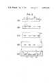
- FIG. 3is a front perspective view of an ink jet multi-nozzle manufactured in the method of the invention.
- FIG. 4is a cross-sectional view of an ink jet multi-nozzle manufactured in the method of the invention which has been mounted for etching.
- a mask 10is placed in close contact with the ⁇ 100> surface 1 of a silicon single crystal. Impurities are diffused into exposed regions 11 of the ⁇ 100> surface 1 which are not covered by the mask 10, forming etching resistive layers 5 shown in FIG. 2(b).
- a silicon crystal 13is grown onto the silicon surface thus treated (FIG. 2(c)), to form a silicon single crystal laminated body. The silicon single crystal laminated body thus formed is then subjected to an etching process.
- FIGS. 2(a)-2(c)a silicon crystal 12 of 0.1 mm in thickness is provided and Boron is diffused into the regions of the ⁇ 100> surface of the silicon crystal which are not covered by the mask 10.
- reference numeral 6designates regions where no impurities are diffused. The regions 6 correspond to the upper openings 1 in FIG. 1 at an opening width (A).
- a second single silicon crystal 13is then grown to a 0.7 mm height above the diffused layers 5, burying the diffused layers in the newly formed wafer as shown in FIG. 2(c).
- An etching mask 7, shown in FIG. 2(d)is placed on the upper surface of the wafer, to form a common groove for the nozzles.
- An etching solutionis prepared by mixing ethylene diamine, pyrocatecol and water in the following rates:
- anisotropic etchingoccurs. That is, the etching 8 first advances uniformly to the buried layers 5 as indicated in FIG. 2(e). The etching then advances past the buried impurity layers 5, which perform as masks, to form an array of nozzles 9-1, 9-2 and 9-3 with a pitch of 0.25 mm. A perspective view of the nozzle array thus formed is illustrated in FIG. 3.
- the thickness of the silicon wafercan be maintained at 0.8 mm; that is, by virtue of the grown silicon crystal, the thickness of the wafer is no longer constrained by the high concentration of nozzles which greatly enhances the mechanical strength of the wafer.
- the wafer according to the invention in FIG. 2(d)can now be readily mounted in an etching bath as shown in FIG. 4 without the probability of etching liquid escape, which existed in the conventional silicon nozzles. Also, a sufficiently high concentration of nozzles per millimeter can be maintained, without compromising the mechanical strength of the nozzle wafer.
Landscapes
- Engineering & Computer Science (AREA)
- Manufacturing & Machinery (AREA)
- Chemical & Material Sciences (AREA)
- Analytical Chemistry (AREA)
- Microelectronics & Electronic Packaging (AREA)
- Particle Formation And Scattering Control In Inkjet Printers (AREA)
Abstract
Description
This invention relates to a silicon nozzle formation method in which a multi-nozzle for an ink jet printer is formed, utilizing the anisotropic etching properties of single crystal silicons. The invention is particularly adopted to increasing the strength and overall utility of nozzles thus formed.
An ink jet multi-nozzle manufacturing method has been proposed in the art, in which, as shown in FIG. 1(a), a silicon single crystal is subjected to etching after a mask is placed on the <100> surface thereof exposing only the area (A). Due to the anisotropic etching properties of such silicon crystals, the resulting multi-nozzle is readily formed and is generally of high quality. Referring to FIG. 1(a), the etching angle θ is set to 54.7° in order to maximize the anisotropy of the silicon crystal. In order to formnozzles 3 at a small pitch, it is therefore necessary that the maximum thickness T of a single crystal silicon plate be equal to the nozzle pitch. For instance, in order to obtain a nozzle pitch of four nozzles per millimeter (mm), the thickness of the single crystal silicon plate should be of the order of 0.1 to 0.2 mm, taking into account the width (B) of each nozzle at its opening.
When the single crystal silicon plate is subjected to anisotropic etching, the singlecrystal silicon plate 12 is mounted on aholder 19 as shown in FIG. 1(b), and is fixed withretainers 20. Anetching solution 17 is then applied to thesingle crystal plate 12. Under the above-described circumstances, due to the fact that thecrystal plate 12 is of small width, it is impossible to sufficiently tighten thecrystal plate 12 with theretainers 20. This in turn creates the probability of the etching solution leaking into the crystal plate at points other than those intended, i.e., other than the exposed portions that have not been masked.
Accordingly, this invention is intended to provide a method of forming an ink jet multi-nozzle in which the above-described drawbacks accompanying a conventional method are eliminated. The foregoing object of the invention has been achieved by the provision of an ink jet multi-nozzle which is made of a single silicon crystal, and in which a common groove for all nozzles forming the multi-nozzle is cut into one surface of the multi-nozzle body. The groove constrains the etchant to the wafer and precluding leaking. The nozzles have openings at the bottom of this common groove, while providing an ink jetting surface which retains the aforementioned attributes of high quality and ready formation.
FIG. 1(a) is a cross-sectional view of an ink jet multi-nozzle which has been manufactured in the conventional method;
FIG. 1(b) is a cross-sectional view of a conventional ink jet multi-nozzle which has been mounted for etching;
FIGS. 2(a)-2(e), are step diagrams that detail the manufacture of an ink jet multi-nozzle according to the method of the invention;
FIG. 3 is a front perspective view of an ink jet multi-nozzle manufactured in the method of the invention; and
FIG. 4 is a cross-sectional view of an ink jet multi-nozzle manufactured in the method of the invention which has been mounted for etching.
One embodiment of this invention will be described in detail with reference to FIGS. 2 through 4.
As shown in FIG. 2(a), amask 10 is placed in close contact with the <100> surface 1 of a silicon single crystal. Impurities are diffused into exposedregions 11 of the <100> surface 1 which are not covered by themask 10, forming etchingresistive layers 5 shown in FIG. 2(b). Asilicon crystal 13 is grown onto the silicon surface thus treated (FIG. 2(c)), to form a silicon single crystal laminated body. The silicon single crystal laminated body thus formed is then subjected to an etching process. Referring now in more detail to FIGS. 2(a)-2(c), asilicon crystal 12 of 0.1 mm in thickness is provided and Boron is diffused into the regions of the <100> surface of the silicon crystal which are not covered by themask 10. This diffusion formsP+ layers 5 and achieves a density of nozzles at four nozzles/mm. In FIG. 2(b),reference numeral 6 designates regions where no impurities are diffused. Theregions 6 correspond to the upper openings 1 in FIG. 1 at an opening width (A).
A secondsingle silicon crystal 13 is then grown to a 0.7 mm height above the diffusedlayers 5, burying the diffused layers in the newly formed wafer as shown in FIG. 2(c). Anetching mask 7, shown in FIG. 2(d), is placed on the upper surface of the wafer, to form a common groove for the nozzles. An etching solution is prepared by mixing ethylene diamine, pyrocatecol and water in the following rates:
ethylene diamine--3.125 ml
pyrocatecol--0.5 g
water--1 ml
By the application of the etching solution thus prepared to the wafer, anisotropic etching occurs. That is, theetching 8 first advances uniformly to the buriedlayers 5 as indicated in FIG. 2(e). The etching then advances past the buriedimpurity layers 5, which perform as masks, to form an array of nozzles 9-1, 9-2 and 9-3 with a pitch of 0.25 mm. A perspective view of the nozzle array thus formed is illustrated in FIG. 3.
As is apparent from FIG. 2(e), the thickness of the silicon wafer can be maintained at 0.8 mm; that is, by virtue of the grown silicon crystal, the thickness of the wafer is no longer constrained by the high concentration of nozzles which greatly enhances the mechanical strength of the wafer.
The wafer according to the invention in FIG. 2(d) can now be readily mounted in an etching bath as shown in FIG. 4 without the probability of etching liquid escape, which existed in the conventional silicon nozzles. Also, a sufficiently high concentration of nozzles per millimeter can be maintained, without compromising the mechanical strength of the nozzle wafer.
Claims (6)
1. A method for the formation of a multi-nozzle ink jet, comprising the steps of:
masking the surface of a single crystal silicon plate;
diffusing impurities onto the unmasked regions of said plate to render said unmasked regions resistant to known etching compositions;
growing a second single crystal silicon plate onto said first single crystal silicon plate;
masking the surface of said second single crystal silicon plate; and
diffusing an etching composition onto said masked second single crystal silicon plate, whereby said etching composition creates an opening in said second single crystal silicon plate, and creates a plurality of nozzles in said first single crystal silicon plate.
2. The novel method of formation of a multi-nozzle ink jet as in claim 1, wherein said first single crystal silicon plate has a thickness substantially equal to the pitch of said plurality of nozzles.
3. The method for the formation of a multi-nozzle ink jet as in claim 1, wherein said first single crystal silicon plate is of approximately 0.1 to 0.2 mm in thickness and said second single crystal silicon plate is of approximately 0.6 to 0.9 mm in thickness.
4. The method for the formation of a multi-nozzle ink jet as in claim 1, wherein said impurities diffused onto said first single crystal silicon plate comprise boron to form P+ regions.
5. The method for the formation of a multi-nozzle ink jet as in claim 1, wherein said etching composition comprises water, ethylene diamine and pyrocatecol.
6. The method for the formation of the multi-nozzle ink jet as in claim 1, wherein said plurality of nozzles created in said first single crystal silicon plate have a pitch of approximately 0.25 mm and have a concentration of 6 to 10 nozzles per millimeter of length.
Applications Claiming Priority (2)
| Application Number | Priority Date | Filing Date | Title |
|---|---|---|---|
| JP56068802AJPS57182449A (en) | 1981-05-07 | 1981-05-07 | Forming method of ink jet multinozzle |
| JP56-68802 | 1981-05-07 |
Publications (1)
| Publication Number | Publication Date |
|---|---|
| US4455192Atrue US4455192A (en) | 1984-06-19 |
Family
ID=13384208
Family Applications (1)
| Application Number | Title | Priority Date | Filing Date |
|---|---|---|---|
| US06/365,923Expired - LifetimeUS4455192A (en) | 1981-05-07 | 1982-04-05 | Formation of a multi-nozzle ink jet |
Country Status (2)
| Country | Link |
|---|---|
| US (1) | US4455192A (en) |
| JP (1) | JPS57182449A (en) |
Cited By (44)
| Publication number | Priority date | Publication date | Assignee | Title |
|---|---|---|---|---|
| US4628576A (en)* | 1985-02-21 | 1986-12-16 | Ford Motor Company | Method for fabricating a silicon valve |
| US4647013A (en)* | 1985-02-21 | 1987-03-03 | Ford Motor Company | Silicon valve |
| US4685185A (en)* | 1986-08-29 | 1987-08-11 | Tektronix, Inc. | Method of manufacturing an ink jet head |
| EP0178596A3 (en)* | 1984-10-15 | 1987-09-16 | At & T Teletype Corporation | Silicon nozzle structures and method of manufacture |
| US4768751A (en)* | 1987-10-19 | 1988-09-06 | Ford Motor Company | Silicon micromachined non-elastic flow valves |
| US4957592A (en)* | 1989-12-27 | 1990-09-18 | Xerox Corporation | Method of using erodable masks to produce partially etched structures in ODE wafer structures |
| US5136344A (en)* | 1988-11-02 | 1992-08-04 | Universal Energy Systems, Inc. | High energy ion implanted silicon on insulator structure |
| US5141596A (en)* | 1991-07-29 | 1992-08-25 | Xerox Corporation | Method of fabricating an ink jet printhead having integral silicon filter |
| US5160577A (en)* | 1991-07-30 | 1992-11-03 | Deshpande Narayan V | Method of fabricating an aperture plate for a roof-shooter type printhead |
| US5204690A (en)* | 1991-07-01 | 1993-04-20 | Xerox Corporation | Ink jet printhead having intergral silicon filter |
| US5487483A (en)* | 1994-05-24 | 1996-01-30 | Xerox Corporation | Nozzles for ink jet devices and method for microfabrication of the nozzles |
| US5492277A (en)* | 1993-02-17 | 1996-02-20 | Nippondenso Co., Ltd. | Fluid injection nozzle |
| US5565113A (en)* | 1994-05-18 | 1996-10-15 | Xerox Corporation | Lithographically defined ejection units |
| US5564392A (en)* | 1994-05-17 | 1996-10-15 | Nippondenso Co., Ltd. | Fluid injection nozzle and fuel injection valve using the same |
| WO1996032285A1 (en)* | 1995-04-12 | 1996-10-17 | Eastman Kodak Company | A self-aligned construction and manufacturing process for monolithic print heads |
| US5901425A (en)* | 1996-08-27 | 1999-05-11 | Topaz Technologies Inc. | Inkjet print head apparatus |
| US5989445A (en)* | 1995-06-09 | 1999-11-23 | The Regents Of The University Of Michigan | Microchannel system for fluid delivery |
| US6019907A (en)* | 1997-08-08 | 2000-02-01 | Hewlett-Packard Company | Forming refill for monolithic inkjet printhead |
| US6045710A (en)* | 1995-04-12 | 2000-04-04 | Silverbrook; Kia | Self-aligned construction and manufacturing process for monolithic print heads |
| EP0999049A3 (en)* | 1998-11-02 | 2000-11-22 | Xerox Corporation | Acoustic printhead and photoetching of acoustic lenses for acoustic ink printing |
| WO2000078668A1 (en)* | 1999-06-22 | 2000-12-28 | President And Fellows Of Harvard College | Control of solid state dimensional features |
| US6189214B1 (en) | 1996-07-08 | 2001-02-20 | Corning Incorporated | Gas-assisted atomizing devices and methods of making gas-assisted atomizing devices |
| US6189813B1 (en) | 1996-07-08 | 2001-02-20 | Corning Incorporated | Rayleigh-breakup atomizing devices and methods of making rayleigh-breakup atomizing devices |
| US6290861B1 (en)* | 1997-07-15 | 2001-09-18 | Silverbrook Research Pty Ltd | Method of manufacture of a conductive PTFE bend actuator vented ink jet printer |
| US6352209B1 (en) | 1996-07-08 | 2002-03-05 | Corning Incorporated | Gas assisted atomizing devices and methods of making gas-assisted atomizing devices |
| US6464842B1 (en) | 1999-06-22 | 2002-10-15 | President And Fellows Of Harvard College | Control of solid state dimensional features |
| US20030066749A1 (en)* | 1999-06-22 | 2003-04-10 | President And Fellows Of Harvard College | Control of solid state dimensional features |
| US20030201245A1 (en)* | 2002-04-30 | 2003-10-30 | Chien-Hua Chen | Substrate and method forming substrate for fluid ejection device |
| US20040055996A1 (en)* | 1999-03-25 | 2004-03-25 | Fuji Xerox Co., Ltd. | Ink jet recording head and method for manufacturing the same |
| US20040229386A1 (en)* | 1999-06-22 | 2004-11-18 | President And Fellows Of Harvard College | Controlled fabrication of gaps in electrically conducting structures |
| US20050006224A1 (en)* | 1999-06-22 | 2005-01-13 | President And Fellows Of Harvard College | Pulsed ion beam control of solid state features |
| US20050269289A1 (en)* | 2004-06-08 | 2005-12-08 | Yoshihide Matsuo | Method of manufacturing a nozzle plate |
| US7258838B2 (en) | 1999-06-22 | 2007-08-21 | President And Fellows Of Harvard College | Solid state molecular probe device |
| US20080208283A1 (en)* | 2007-02-26 | 2008-08-28 | Rio Vetter | Neural Interface System |
| US20080257859A1 (en)* | 2005-04-06 | 2008-10-23 | President And Fellows Of Harvard College | Molecular characterization with carbon nanotube control |
| US20090118806A1 (en)* | 2007-10-17 | 2009-05-07 | Vetter Rio J | Three-dimensional system of electrode leads |
| US20090132042A1 (en)* | 2007-10-17 | 2009-05-21 | Hetke Jamille F | Implantable device including a resorbable carrier |
| US20090187196A1 (en)* | 2007-10-17 | 2009-07-23 | Vetter Rio J | Guide tube for an implantable device system |
| US20090234426A1 (en)* | 2008-02-29 | 2009-09-17 | Pellinen David S | Implantable electrode and method of making the same |
| US20110093052A1 (en)* | 2009-10-16 | 2011-04-21 | Anderson David J | Neural interface system |
| CN102079504A (en)* | 2010-12-07 | 2011-06-01 | 清华大学 | Method for manufacturing high-density silicon-based nano-holes |
| US20110154655A1 (en)* | 2005-10-07 | 2011-06-30 | Hetke Jamille F | Modular multichannel microelectrode array and methods of making same |
| US20140354735A1 (en)* | 2013-05-31 | 2014-12-04 | Stmicroelectronics, Inc. | Method of making inkjet print heads having inkjet chambers and orifices formed in a wafer and related devices |
| US9155861B2 (en) | 2010-09-20 | 2015-10-13 | Neuronexus Technologies, Inc. | Neural drug delivery system with fluidic threads |
Families Citing this family (4)
| Publication number | Priority date | Publication date | Assignee | Title |
|---|---|---|---|---|
| JPH0729414B2 (en)* | 1987-01-22 | 1995-04-05 | 株式会社テック | Valve element and manufacturing method thereof |
| US5208980A (en)* | 1991-12-31 | 1993-05-11 | Compag Computer Corporation | Method of forming tapered orifice arrays in fully assembled ink jet printheads |
| JP2932877B2 (en)* | 1992-02-06 | 1999-08-09 | セイコーエプソン株式会社 | Method of manufacturing inkjet head |
| US5703631A (en)* | 1992-05-05 | 1997-12-30 | Compaq Computer Corporation | Method of forming an orifice array for a high density ink jet printhead |
Citations (8)
| Publication number | Priority date | Publication date | Assignee | Title |
|---|---|---|---|---|
| US3921916A (en)* | 1974-12-31 | 1975-11-25 | Ibm | Nozzles formed in monocrystalline silicon |
| JPS5267271A (en)* | 1975-12-01 | 1977-06-03 | Fujitsu Ltd | Formation of through-hole onto semiconductor substrate |
| JPS5267273A (en)* | 1975-12-01 | 1977-06-03 | Fujitsu Ltd | Formation of through-hole onto semiconductor substrate |
| JPS5549275A (en)* | 1978-10-06 | 1980-04-09 | Fuji Xerox Co Ltd | Multi-nozzle orifice plate |
| US4256532A (en)* | 1977-07-05 | 1981-03-17 | International Business Machines Corporation | Method for making a silicon mask |
| US4282533A (en)* | 1980-02-22 | 1981-08-04 | Celanese Corporation | Precision orifice nozzle devices for ink jet printing apparati and the process for their manufacture |
| US4381341A (en)* | 1982-02-01 | 1983-04-26 | Westinghouse Electric Corp. | Two stage etching process for through the substrate contacts |
| US4417946A (en)* | 1979-06-01 | 1983-11-29 | International Business Machines Corporation | Method of making mask for structuring surface areas |
- 1981
- 1981-05-07JPJP56068802Apatent/JPS57182449A/enactivePending
- 1982
- 1982-04-05USUS06/365,923patent/US4455192A/ennot_activeExpired - Lifetime
Patent Citations (8)
| Publication number | Priority date | Publication date | Assignee | Title |
|---|---|---|---|---|
| US3921916A (en)* | 1974-12-31 | 1975-11-25 | Ibm | Nozzles formed in monocrystalline silicon |
| JPS5267271A (en)* | 1975-12-01 | 1977-06-03 | Fujitsu Ltd | Formation of through-hole onto semiconductor substrate |
| JPS5267273A (en)* | 1975-12-01 | 1977-06-03 | Fujitsu Ltd | Formation of through-hole onto semiconductor substrate |
| US4256532A (en)* | 1977-07-05 | 1981-03-17 | International Business Machines Corporation | Method for making a silicon mask |
| JPS5549275A (en)* | 1978-10-06 | 1980-04-09 | Fuji Xerox Co Ltd | Multi-nozzle orifice plate |
| US4417946A (en)* | 1979-06-01 | 1983-11-29 | International Business Machines Corporation | Method of making mask for structuring surface areas |
| US4282533A (en)* | 1980-02-22 | 1981-08-04 | Celanese Corporation | Precision orifice nozzle devices for ink jet printing apparati and the process for their manufacture |
| US4381341A (en)* | 1982-02-01 | 1983-04-26 | Westinghouse Electric Corp. | Two stage etching process for through the substrate contacts |
Non-Patent Citations (4)
| Title |
|---|
| Bassous, "High Density . . . Silicon", IBM Technical Disclosure Bulletin, vol. 19, No. 6, (11/76), pp. 2251-2252. |
| Bassous, High Density . . . Silicon , IBM Technical Disclosure Bulletin, vol. 19, No. 6, (11/76), pp. 2251 2252.* |
| Chiou et al., "Ink Jet Nozzles", IBM Technical Disclosure Bulletin, vol. 19, No. 9, (2/77), p. 3569. |
| Chiou et al., Ink Jet Nozzles , IBM Technical Disclosure Bulletin, vol. 19, No. 9, (2/77), p. 3569.* |
Cited By (75)
| Publication number | Priority date | Publication date | Assignee | Title |
|---|---|---|---|---|
| EP0178596A3 (en)* | 1984-10-15 | 1987-09-16 | At & T Teletype Corporation | Silicon nozzle structures and method of manufacture |
| US4628576A (en)* | 1985-02-21 | 1986-12-16 | Ford Motor Company | Method for fabricating a silicon valve |
| US4647013A (en)* | 1985-02-21 | 1987-03-03 | Ford Motor Company | Silicon valve |
| US4685185A (en)* | 1986-08-29 | 1987-08-11 | Tektronix, Inc. | Method of manufacturing an ink jet head |
| US4768751A (en)* | 1987-10-19 | 1988-09-06 | Ford Motor Company | Silicon micromachined non-elastic flow valves |
| US5136344A (en)* | 1988-11-02 | 1992-08-04 | Universal Energy Systems, Inc. | High energy ion implanted silicon on insulator structure |
| US4957592A (en)* | 1989-12-27 | 1990-09-18 | Xerox Corporation | Method of using erodable masks to produce partially etched structures in ODE wafer structures |
| US5204690A (en)* | 1991-07-01 | 1993-04-20 | Xerox Corporation | Ink jet printhead having intergral silicon filter |
| US5141596A (en)* | 1991-07-29 | 1992-08-25 | Xerox Corporation | Method of fabricating an ink jet printhead having integral silicon filter |
| US5160577A (en)* | 1991-07-30 | 1992-11-03 | Deshpande Narayan V | Method of fabricating an aperture plate for a roof-shooter type printhead |
| US5492277A (en)* | 1993-02-17 | 1996-02-20 | Nippondenso Co., Ltd. | Fluid injection nozzle |
| US5564392A (en)* | 1994-05-17 | 1996-10-15 | Nippondenso Co., Ltd. | Fluid injection nozzle and fuel injection valve using the same |
| US5565113A (en)* | 1994-05-18 | 1996-10-15 | Xerox Corporation | Lithographically defined ejection units |
| US5487483A (en)* | 1994-05-24 | 1996-01-30 | Xerox Corporation | Nozzles for ink jet devices and method for microfabrication of the nozzles |
| US6045710A (en)* | 1995-04-12 | 2000-04-04 | Silverbrook; Kia | Self-aligned construction and manufacturing process for monolithic print heads |
| WO1996032285A1 (en)* | 1995-04-12 | 1996-10-17 | Eastman Kodak Company | A self-aligned construction and manufacturing process for monolithic print heads |
| US5989445A (en)* | 1995-06-09 | 1999-11-23 | The Regents Of The University Of Michigan | Microchannel system for fluid delivery |
| US6513736B1 (en) | 1996-07-08 | 2003-02-04 | Corning Incorporated | Gas-assisted atomizing device and methods of making gas-assisted atomizing devices |
| US6378788B1 (en)* | 1996-07-08 | 2002-04-30 | Corning Incorporated | Rayleigh-breakup atomizing devices and methods of making rayleigh-breakup atomizing devices |
| US6352209B1 (en) | 1996-07-08 | 2002-03-05 | Corning Incorporated | Gas assisted atomizing devices and methods of making gas-assisted atomizing devices |
| US6189214B1 (en) | 1996-07-08 | 2001-02-20 | Corning Incorporated | Gas-assisted atomizing devices and methods of making gas-assisted atomizing devices |
| US6189813B1 (en) | 1996-07-08 | 2001-02-20 | Corning Incorporated | Rayleigh-breakup atomizing devices and methods of making rayleigh-breakup atomizing devices |
| US5901425A (en)* | 1996-08-27 | 1999-05-11 | Topaz Technologies Inc. | Inkjet print head apparatus |
| US6290861B1 (en)* | 1997-07-15 | 2001-09-18 | Silverbrook Research Pty Ltd | Method of manufacture of a conductive PTFE bend actuator vented ink jet printer |
| US6158846A (en)* | 1997-08-08 | 2000-12-12 | Hewlett-Packard Co. | Forming refill for monolithic inkjet printhead |
| US6019907A (en)* | 1997-08-08 | 2000-02-01 | Hewlett-Packard Company | Forming refill for monolithic inkjet printhead |
| EP0999049A3 (en)* | 1998-11-02 | 2000-11-22 | Xerox Corporation | Acoustic printhead and photoetching of acoustic lenses for acoustic ink printing |
| US20040055996A1 (en)* | 1999-03-25 | 2004-03-25 | Fuji Xerox Co., Ltd. | Ink jet recording head and method for manufacturing the same |
| WO2000078668A1 (en)* | 1999-06-22 | 2000-12-28 | President And Fellows Of Harvard College | Control of solid state dimensional features |
| US6464842B1 (en) | 1999-06-22 | 2002-10-15 | President And Fellows Of Harvard College | Control of solid state dimensional features |
| US20030066749A1 (en)* | 1999-06-22 | 2003-04-10 | President And Fellows Of Harvard College | Control of solid state dimensional features |
| US7582490B2 (en) | 1999-06-22 | 2009-09-01 | President And Fellows Of Harvard College | Controlled fabrication of gaps in electrically conducting structures |
| US6783643B2 (en) | 1999-06-22 | 2004-08-31 | President And Fellows Of Harvard College | Control of solid state dimensional features |
| US20040229386A1 (en)* | 1999-06-22 | 2004-11-18 | President And Fellows Of Harvard College | Controlled fabrication of gaps in electrically conducting structures |
| US20050006224A1 (en)* | 1999-06-22 | 2005-01-13 | President And Fellows Of Harvard College | Pulsed ion beam control of solid state features |
| US7258838B2 (en) | 1999-06-22 | 2007-08-21 | President And Fellows Of Harvard College | Solid state molecular probe device |
| US7118657B2 (en) | 1999-06-22 | 2006-10-10 | President And Fellows Of Harvard College | Pulsed ion beam control of solid state features |
| US6981759B2 (en)* | 2002-04-30 | 2006-01-03 | Hewlett-Packard Development Company, Lp. | Substrate and method forming substrate for fluid ejection device |
| US20030201245A1 (en)* | 2002-04-30 | 2003-10-30 | Chien-Hua Chen | Substrate and method forming substrate for fluid ejection device |
| US7282448B2 (en) | 2002-04-30 | 2007-10-16 | Hewlett-Packard Development Company, L.P. | Substrate and method of forming substrate for fluid ejection device |
| US20050282331A1 (en)* | 2002-04-30 | 2005-12-22 | Chien-Hua Chen | Substrate and method of forming substrate for fluid ejection device |
| US20050269289A1 (en)* | 2004-06-08 | 2005-12-08 | Yoshihide Matsuo | Method of manufacturing a nozzle plate |
| US7306744B2 (en)* | 2004-06-08 | 2007-12-11 | Seiko Epson Corporation | Method of manufacturing a nozzle plate |
| CN100389958C (en)* | 2004-06-08 | 2008-05-28 | 精工爱普生株式会社 | Method of manufacturing nozzle plate |
| US20080257859A1 (en)* | 2005-04-06 | 2008-10-23 | President And Fellows Of Harvard College | Molecular characterization with carbon nanotube control |
| US8092697B2 (en) | 2005-04-06 | 2012-01-10 | President And Fellows Of Harvard College | Molecular characterization with carbon nanotube control |
| US8800140B2 (en) | 2005-10-07 | 2014-08-12 | Neuronexus Technologies, Inc. | Method of making a modular multichannel microelectrode array |
| US20110154655A1 (en)* | 2005-10-07 | 2011-06-30 | Hetke Jamille F | Modular multichannel microelectrode array and methods of making same |
| US9604051B2 (en) | 2007-02-26 | 2017-03-28 | Medtronic Bakken Research Center B.V. | Neural interface system |
| US8731673B2 (en) | 2007-02-26 | 2014-05-20 | Sapiens Steering Brain Stimulation B.V. | Neural interface system |
| US20080208283A1 (en)* | 2007-02-26 | 2008-08-28 | Rio Vetter | Neural Interface System |
| US11324945B2 (en) | 2007-02-26 | 2022-05-10 | Medtronic Bakken Research Center B.V. | Neural interface system |
| US10357649B2 (en) | 2007-02-26 | 2019-07-23 | Medtronic Bakken Research Center B.V. | Neural interface system |
| US11690548B2 (en) | 2007-10-17 | 2023-07-04 | Neuronexus Technologies, Inc. | Method for implanting an implantable device in body tissue |
| US8224417B2 (en) | 2007-10-17 | 2012-07-17 | Neuronexus Technologies, Inc. | Guide tube for an implantable device system |
| US10034615B2 (en) | 2007-10-17 | 2018-07-31 | Neuronexus Technologies, Inc. | Method for implanting an implantable device in body tissue |
| US20090118806A1 (en)* | 2007-10-17 | 2009-05-07 | Vetter Rio J | Three-dimensional system of electrode leads |
| US8565894B2 (en) | 2007-10-17 | 2013-10-22 | Neuronexus Technologies, Inc. | Three-dimensional system of electrode leads |
| US8958862B2 (en) | 2007-10-17 | 2015-02-17 | Neuronexus Technologies, Inc. | Implantable device including a resorbable carrier |
| US20090187196A1 (en)* | 2007-10-17 | 2009-07-23 | Vetter Rio J | Guide tube for an implantable device system |
| US8805468B2 (en) | 2007-10-17 | 2014-08-12 | Neuronexus Technologies, Inc. | Guide tube for an implantable device system |
| US20090132042A1 (en)* | 2007-10-17 | 2009-05-21 | Hetke Jamille F | Implantable device including a resorbable carrier |
| US8498720B2 (en) | 2008-02-29 | 2013-07-30 | Neuronexus Technologies, Inc. | Implantable electrode and method of making the same |
| US9265928B2 (en) | 2008-02-29 | 2016-02-23 | Greatbatch Ltd. | Implantable electrode and method of making the same |
| US9656054B2 (en) | 2008-02-29 | 2017-05-23 | Neuronexus Technologies, Inc. | Implantable electrode and method of making the same |
| US10688298B2 (en) | 2008-02-29 | 2020-06-23 | Neuronexus Technologies, Inc. | Implantable electrode and method of making the same |
| US20090234426A1 (en)* | 2008-02-29 | 2009-09-17 | Pellinen David S | Implantable electrode and method of making the same |
| US8332046B2 (en) | 2009-10-16 | 2012-12-11 | Neuronexus Technologies, Inc. | Neural interface system |
| US20110093052A1 (en)* | 2009-10-16 | 2011-04-21 | Anderson David J | Neural interface system |
| US9155861B2 (en) | 2010-09-20 | 2015-10-13 | Neuronexus Technologies, Inc. | Neural drug delivery system with fluidic threads |
| CN102079504A (en)* | 2010-12-07 | 2011-06-01 | 清华大学 | Method for manufacturing high-density silicon-based nano-holes |
| US9308728B2 (en)* | 2013-05-31 | 2016-04-12 | Stmicroelectronics, Inc. | Method of making inkjet print heads having inkjet chambers and orifices formed in a wafer and related devices |
| US20140354735A1 (en)* | 2013-05-31 | 2014-12-04 | Stmicroelectronics, Inc. | Method of making inkjet print heads having inkjet chambers and orifices formed in a wafer and related devices |
| US10124588B2 (en) | 2013-05-31 | 2018-11-13 | Stmicroelectronics, Inc. | Method of making inkjet print heads having inkjet chambers and orifices formed in a wafer and related devices |
| US10843465B2 (en) | 2013-05-31 | 2020-11-24 | Stmicroelectronics, Inc. | Method of making inkjet print heads having inkjet chambers and orifices formed in a wafer and related devices |
Also Published As
| Publication number | Publication date |
|---|---|
| JPS57182449A (en) | 1982-11-10 |
Similar Documents
| Publication | Publication Date | Title |
|---|---|---|
| US4455192A (en) | Formation of a multi-nozzle ink jet | |
| DE68918982T2 (en) | Method for separating integrated circuits on a substrate. | |
| US4733823A (en) | Silicon nozzle structures and method of manufacture | |
| CA1037519A (en) | Method of producing nozzles in monocrystalline silicon wafer | |
| CA1040322A (en) | Method of making a semiconductor structure using backside exposure | |
| JPS57204133A (en) | Manufacture of semiconductor integrated circuit | |
| DE102005038152A1 (en) | Semiconductor component and method for its production | |
| US5096535A (en) | Process for manufacturing segmented channel structures | |
| US5716533A (en) | Method of fabricating ink jet printheads | |
| KR930009109B1 (en) | Silicon nozzle structure | |
| JPS6043309B2 (en) | Multi nozzle orifice plate | |
| EP1378363A2 (en) | Method for making through-hole and ink-jet printer head fabricated using the method | |
| GB2095897A (en) | Semiconductor manufacture | |
| JPS644019A (en) | Manufacture of semiconductor device | |
| JPS55105332A (en) | Manufacture of semiconductor device | |
| JPS5515230A (en) | Semiconductor device and its manufacturing method | |
| JPS54109783A (en) | Manufacture of semiconductor device | |
| JPS57143862A (en) | Manufacture of semiconductor integrated circuit | |
| JPS55102240A (en) | Manufacture of semiconductor device | |
| JPS57122570A (en) | Forming method for impurity region in semiconductor | |
| CA1065981A (en) | Production of high radiance light emitting diodes | |
| JPS5635458A (en) | Manufacture of integrated circuit device | |
| JP3219867B2 (en) | Jet nozzle and manufacturing method thereof | |
| JPS5489594A (en) | Manufacture for integrated circuit | |
| JPS62209829A (en) | Manufacture of mesa-type semiconductor device |
Legal Events
| Date | Code | Title | Description |
|---|---|---|---|
| AS | Assignment | Owner name:FUJI XEROX CO., LTD. NO. 3-5, AKASAKA 3-CHOME, MIN Free format text:ASSIGNMENT OF ASSIGNORS INTEREST.;ASSIGNOR:TAMAI, MASAYOSHI;REEL/FRAME:004242/0450 Effective date:19820318 | |
| STCF | Information on status: patent grant | Free format text:PATENTED CASE | |
| FEPP | Fee payment procedure | Free format text:PAYOR NUMBER ASSIGNED (ORIGINAL EVENT CODE: ASPN); ENTITY STATUS OF PATENT OWNER: LARGE ENTITY | |
| FPAY | Fee payment | Year of fee payment:4 | |
| FPAY | Fee payment | Year of fee payment:8 | |
| FEPP | Fee payment procedure | Free format text:PAYER NUMBER DE-ASSIGNED (ORIGINAL EVENT CODE: RMPN); ENTITY STATUS OF PATENT OWNER: LARGE ENTITY Free format text:PAYOR NUMBER ASSIGNED (ORIGINAL EVENT CODE: ASPN); ENTITY STATUS OF PATENT OWNER: LARGE ENTITY | |
| FPAY | Fee payment | Year of fee payment:12 |