US4450461A - Low cost high isolation voltage optocoupler with improved light transmissivity - Google Patents
Low cost high isolation voltage optocoupler with improved light transmissivityDownload PDFInfo
- Publication number
- US4450461A US4450461AUS06/286,628US28662881AUS4450461AUS 4450461 AUS4450461 AUS 4450461AUS 28662881 AUS28662881 AUS 28662881AUS 4450461 AUS4450461 AUS 4450461A
- Authority
- US
- United States
- Prior art keywords
- emitter
- detector
- rod
- coupling
- light
- Prior art date
- Legal status (The legal status is an assumption and is not a legal conclusion. Google has not performed a legal analysis and makes no representation as to the accuracy of the status listed.)
- Expired - Fee Related
Links
- 238000002955isolationMethods0.000titleclaimsabstractdescription12
- 230000008878couplingEffects0.000claimsabstractdescription47
- 238000010168coupling processMethods0.000claimsabstractdescription47
- 238000005859coupling reactionMethods0.000claimsabstractdescription47
- 239000000463materialSubstances0.000claimsdescription29
- 239000004065semiconductorSubstances0.000claimsdescription9
- 239000011521glassSubstances0.000claimsdescription5
- 239000000758substrateSubstances0.000claims3
- 239000003989dielectric materialSubstances0.000abstractdescription7
- 239000011248coating agentSubstances0.000abstractdescription6
- 238000000576coating methodMethods0.000abstractdescription6
- 239000008188pelletSubstances0.000description34
- 230000015556catabolic processEffects0.000description9
- 238000000034methodMethods0.000description8
- 230000001965increasing effectEffects0.000description7
- 238000004519manufacturing processMethods0.000description7
- 230000003287optical effectEffects0.000description7
- 239000004593EpoxySubstances0.000description6
- 238000013459approachMethods0.000description6
- 230000008901benefitEffects0.000description5
- 229920001296polysiloxanePolymers0.000description5
- GWEVSGVZZGPLCZ-UHFFFAOYSA-NTitan oxideChemical compoundO=[Ti]=OGWEVSGVZZGPLCZ-UHFFFAOYSA-N0.000description4
- 238000000465mouldingMethods0.000description4
- 238000012546transferMethods0.000description4
- 230000005540biological transmissionEffects0.000description3
- 150000001875compoundsChemical class0.000description3
- 238000010276constructionMethods0.000description3
- 239000007788liquidSubstances0.000description3
- 238000012986modificationMethods0.000description3
- 230000004048modificationEffects0.000description3
- 229920002379silicone rubberPolymers0.000description3
- 239000004945silicone rubberSubstances0.000description3
- MDPILPRLPQYEEN-UHFFFAOYSA-Naluminium arsenideChemical compound[As]#[Al]MDPILPRLPQYEEN-UHFFFAOYSA-N0.000description2
- 238000005538encapsulationMethods0.000description2
- 230000002708enhancing effectEffects0.000description2
- 238000010438heat treatmentMethods0.000description2
- 230000008520organizationEffects0.000description2
- 238000012360testing methodMethods0.000description2
- 239000004408titanium dioxideSubstances0.000description2
- JBRZTFJDHDCESZ-UHFFFAOYSA-NAsGaChemical compound[As]#[Ga]JBRZTFJDHDCESZ-UHFFFAOYSA-N0.000description1
- 229910001218Gallium arsenideInorganic materials0.000description1
- ATJFFYVFTNAWJD-UHFFFAOYSA-NTinChemical compound[Sn]ATJFFYVFTNAWJD-UHFFFAOYSA-N0.000description1
- 239000000853adhesiveSubstances0.000description1
- 230000001070adhesive effectEffects0.000description1
- 239000000956alloySubstances0.000description1
- 229910045601alloyInorganic materials0.000description1
- 238000013461designMethods0.000description1
- 238000006073displacement reactionMethods0.000description1
- 230000000694effectsEffects0.000description1
- 238000002839fiber optic waveguideMethods0.000description1
- 230000009969flowable effectEffects0.000description1
- 239000000203mixtureSubstances0.000description1
- 239000004033plasticSubstances0.000description1
- 230000001681protective effectEffects0.000description1
- 230000009467reductionEffects0.000description1
- 239000012858resilient materialSubstances0.000description1
- 230000004044responseEffects0.000description1
- 230000035945sensitivityEffects0.000description1
- 238000005476solderingMethods0.000description1
- 230000002459sustained effectEffects0.000description1
- 238000003466weldingMethods0.000description1
Images

Classifications
- G—PHYSICS
- G02—OPTICS
- G02B—OPTICAL ELEMENTS, SYSTEMS OR APPARATUS
- G02B6/00—Light guides; Structural details of arrangements comprising light guides and other optical elements, e.g. couplings
- G02B6/24—Coupling light guides
- G02B6/42—Coupling light guides with opto-electronic elements
- G02B6/4295—Coupling light guides with opto-electronic elements coupling with semiconductor devices activated by light through the light guide, e.g. thyristors, phototransistors
- H—ELECTRICITY
- H10—SEMICONDUCTOR DEVICES; ELECTRIC SOLID-STATE DEVICES NOT OTHERWISE PROVIDED FOR
- H10F—INORGANIC SEMICONDUCTOR DEVICES SENSITIVE TO INFRARED RADIATION, LIGHT, ELECTROMAGNETIC RADIATION OF SHORTER WAVELENGTH OR CORPUSCULAR RADIATION
- H10F55/00—Radiation-sensitive semiconductor devices covered by groups H10F10/00, H10F19/00 or H10F30/00 being structurally associated with electric light sources and electrically or optically coupled thereto
- H10F55/20—Radiation-sensitive semiconductor devices covered by groups H10F10/00, H10F19/00 or H10F30/00 being structurally associated with electric light sources and electrically or optically coupled thereto wherein the electric light source controls the radiation-sensitive semiconductor devices, e.g. optocouplers
- H10F55/25—Radiation-sensitive semiconductor devices covered by groups H10F10/00, H10F19/00 or H10F30/00 being structurally associated with electric light sources and electrically or optically coupled thereto wherein the electric light source controls the radiation-sensitive semiconductor devices, e.g. optocouplers wherein the radiation-sensitive devices and the electric light source are all semiconductor devices
- H—ELECTRICITY
- H10—SEMICONDUCTOR DEVICES; ELECTRIC SOLID-STATE DEVICES NOT OTHERWISE PROVIDED FOR
- H10F—INORGANIC SEMICONDUCTOR DEVICES SENSITIVE TO INFRARED RADIATION, LIGHT, ELECTROMAGNETIC RADIATION OF SHORTER WAVELENGTH OR CORPUSCULAR RADIATION
- H10F77/00—Constructional details of devices covered by this subclass
- H10F77/40—Optical elements or arrangements
- H10F77/407—Optical elements or arrangements indirectly associated with the devices
- H—ELECTRICITY
- H01—ELECTRIC ELEMENTS
- H01L—SEMICONDUCTOR DEVICES NOT COVERED BY CLASS H10
- H01L2224/00—Indexing scheme for arrangements for connecting or disconnecting semiconductor or solid-state bodies and methods related thereto as covered by H01L24/00
- H01L2224/01—Means for bonding being attached to, or being formed on, the surface to be connected, e.g. chip-to-package, die-attach, "first-level" interconnects; Manufacturing methods related thereto
- H01L2224/42—Wire connectors; Manufacturing methods related thereto
- H01L2224/47—Structure, shape, material or disposition of the wire connectors after the connecting process
- H01L2224/48—Structure, shape, material or disposition of the wire connectors after the connecting process of an individual wire connector
- H01L2224/4805—Shape
- H01L2224/4809—Loop shape
- H01L2224/48091—Arched
- H—ELECTRICITY
- H01—ELECTRIC ELEMENTS
- H01L—SEMICONDUCTOR DEVICES NOT COVERED BY CLASS H10
- H01L2224/00—Indexing scheme for arrangements for connecting or disconnecting semiconductor or solid-state bodies and methods related thereto as covered by H01L24/00
- H01L2224/01—Means for bonding being attached to, or being formed on, the surface to be connected, e.g. chip-to-package, die-attach, "first-level" interconnects; Manufacturing methods related thereto
- H01L2224/42—Wire connectors; Manufacturing methods related thereto
- H01L2224/47—Structure, shape, material or disposition of the wire connectors after the connecting process
- H01L2224/48—Structure, shape, material or disposition of the wire connectors after the connecting process of an individual wire connector
- H01L2224/481—Disposition
- H01L2224/48151—Connecting between a semiconductor or solid-state body and an item not being a semiconductor or solid-state body, e.g. chip-to-substrate, chip-to-passive
- H01L2224/48221—Connecting between a semiconductor or solid-state body and an item not being a semiconductor or solid-state body, e.g. chip-to-substrate, chip-to-passive the body and the item being stacked
- H01L2224/48245—Connecting between a semiconductor or solid-state body and an item not being a semiconductor or solid-state body, e.g. chip-to-substrate, chip-to-passive the body and the item being stacked the item being metallic
- H01L2224/48247—Connecting between a semiconductor or solid-state body and an item not being a semiconductor or solid-state body, e.g. chip-to-substrate, chip-to-passive the body and the item being stacked the item being metallic connecting the wire to a bond pad of the item
Definitions
- This inventionrelates in general to semiconductor devices and more particularly to a low cost semiconductor optocoupler having improved coupling between the emitter and detector thereof while maintaining high dielectric strength therebetween.
- Optocouplerswhich provide an electrically isolated link between two circuits through the use of an optical emitter and an optical detector which may be operated at vastly different electrical potentials, are employed in power supplies, telecommunications, computer interfacing, control systems, and a wide variety of other applications. While devices of unquestioned utility presently exist for a number of these applications, the use of optocouplers in other applications has thus far been prohibited by a cost-performance tradeoff. While high performance optocouplers have been obtainable, their cost has been likewise high. Low cost couplers while available have been of likewise low performance.
- a significant characteristic of an optocoupleris the isolation voltage, the voltage which can be sustained between the input and output terminals without breakdown. Another important characteristic is the degree of optical coupling between the input and output of the device which is sometimes referred to as the current transfer ratio (CTR) or similar specification.
- CTRcurrent transfer ratio
- the isolation voltage of optocouplersmay be quite readily increased by increasing the spacing between the emitter and detector elements of the coupler since for most materials the dielectric strength increases directly with increased thickness of material. The spacing between the emitter and detector cannot however be increased without limit due inter alia to package constraints and perhaps even more significantly to the reduction in CTR which accompanies a wider spacing of emitter and detector elements.
- a number of approacheshave been used to increase breakdown voltage while at the same time maintaining high CTR.
- a very successful approachhas been the introduction of a layer of glass between the emitter and detector. Glass has a higher dielectric strength than many materials and a relatively thin glass sheet dispossed between the emitter and detector elements provides great dielectric strength and therefore high isolation voltages. Such a construction however is expensive to manufacture and while it provides high performance, both in terms of CTR and isolation voltage, it is not universally applicable due to its relatively high cost.
- Another approach which has been successfulinvolves the use of a so-called light cavity wherein a clear curable dielectric medium is interposed between the emitter and detector elements in an uncured state and then cured during subsequent manufacture. A reflective dielectric medium is formed around the clear medium to cause internal reflection and increase the CTR.
- an object of this inventionto provide an optocoupler having an emitter and detector element widely spaced therein for achieving a high dielectric strength therebetween and high breakdown voltage while at the same time providing heretofore unachieved efficiency of coupling and therefore high CTR between the emitter and detector elements.
- an optocoupler having high isolation voltage and high CTR which is manufactured at low costincludes an optical emitter and an optical detector responsive to light generated by the emitter in response to an electrical input signal thereto.
- the emitter and detectorare respectively coupled to one and another ends of a bar of light transmissive material by intermediate layers of light transmissive coupling material.
- the transmission of light through the bar of light transmissive materialis enhanced in accordance with a preferred embodiment of this invention by the presence of a reflective dielectric coating on the bar which causes the light to be substantially contained within the bar of light transmissive material and therefore to be conducted with great efficiency from the emitter to the detector.
- An opaque dielectric housingsuch as epoxy or silicone molding compound is provided for both eliminating the effects of ambient light on the operation of the optocoupler and for providing mechanical support for the electrical leads thereof.
- the bar of light transmissive dielectric materialmay have a shape selected to further improve the coupling between the emitter and detector and the one and another ends of the bar.
- the inventionalso includes a method for manufacturing an optocoupler in accordance with the teachings thereof which method is particularly low in cost.
- a lead framewhich preferably includes the input leads and output leads of the optocoupler is provided onto which lead frame the emitter and detector pellets are mounted and to the several pins of which lead frame the various electrical connections from the emitter and detector pellets are made.
- the emitter and detector pelletsare coated with a coupling layer of clear light transmissive dielectric material and the light transmissive bar is positioned between the pellets in contact with the coupling layer.
- the light transmissive materialis then preferably cured to provide both a support for the bar and efficient coupling to the ends thereof from the emitter and detector elements.
- a layer of reflective dielectric materialis then applied to the bar as well as to the coupling layers to enhance the transfer of light from the emitter to the detector.
- the reflective dielectric materialis preferably a curable material which is applied in an uncured form and then cured.
- a suitable housing for the devicemay be formed by encapsulating the device in epoxy or in silicone molding compound or the like.
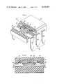
- FIG. 1is a cut-away view of an optocoupler in accordance to this invention.
- FIG. 2is a fragmentary enlarged sectional view of the coupler of FIG. 1.
- FIGS. 3 through 9are detailed sectional views of alternative embodiments of the invention.
- an optocoupler 10 in accordance with this inventionwhich includes first and second opposed sets of spaced apart terminals one set being shown at 12. Each set may include a number of individual terminals within that set such as terminals 20, 22 and 24 of set 12, and terminals 14, 16 of the other set.
- the device of FIGS. 1 and 2will be recognized as taking the form of the so-called dual-in-line package conventionally employed for a wide variety of semiconductor devices.
- the terminalsare conveniently provided during manufacture of the device of FIG. 1 in the form of a lead frame having the individual terminals supported therein by a detachable web of connecting material which is removed after certain fabrication steps employed in manufacturing the device are completed.
- the electrical terminalsremain connected in the lead frame during the mounting of the semiconductor elements thereon and, where desired, through the encapsulation of the device in its outer protective housing after which encapsulation the connecting material may be removed, the terminals being supported by the body of housing material.
- emitter 26 and a detector 28are mounted on terminals 16 and 22, respectively. It is preferred in accordance with this invention that emitter 26 be a semiconductor light emitting diode which is responsive to an electrical input signal to generate a light output signal which light output signal may be a visible light output signal or an infrared light output signal or any other signal to which detector 28 is responsive.
- Detector 28 mounted to an upper surface of terminal 22is selected to be responsive to the light output signal generated by emitter 26 and to produce an electrical output signal.
- detector 28takes the form of a light controlled semiconductor device through whose terminals an electrical output signal flows under control of the light output signal from emitter 26 as detected by detector 28.
- the generation of an electrical output signalshould be understood to mean not only the direct generation of an electrical signal but also the control of an external electrical signal.
- Rod 32may conveniently be manufactured of glass, clear epoxy, plastic, fiber optic waveguide or any other light transmissive material.
- rod 32may have a number of shapes as will be more fully described hereinbelow but is characterized by a generally elongate form to the ends of which the emitter and detector are coupled as distinguished from a plate of optically transmissive dielectric material as has been heretofore employed in certain coupler constructions wherein the transmission of light has been primarily between faces of the plate through the short thickness dimension thereof rather than along a rod of optically transmissive dielectric coupling material as is shown in FIGS. 1 and 2.
- first and second layers of coupling material 31 and 33are disposed between the emitter 26, the detector 28 and their respective ends of rod 32. It is preferred in accordance with this invention to employ a clear curable dielectric material such as clear silicone rubber, epoxy or the like for coupling layers 31 and 33.
- the efficiency of coupling between the emitter and detectormay be greatly enhanced in accordance with this invention by providing on the surface of rod 32 a layer of electrically non-conductive optically reflective material 34 for enhancing the transmission of light from the emitter through rod 32 to the detector.
- Layer 34may preferably take the form of a curable resilient material such as silicone rubber, a reflective epoxy or the like any of which can conveniently be applied to the surface of rod 32 and which may if desired surround all or part of emitter 26, detector 28 and the optically transmissive coupling layers between the emitter and detector and the respective ends of rod 32.
- Reflective layer 34is preferably chosen for its dielectric strength in addition to its reflective characteristics inasmuch as it bridges the gap between input electrical terminal 16 and output terminal 22 and could if of insufficient dielectric strength, provide a breakdown path therebetween. Still further, reflective layer 34 is chosen for its integrity of bonding both to dielectric rod 32 and coupling layers 31 and 33. It will be appreciated that the interfaces between the various elements which make up this invention especially those interfaces which intersect both the input and output terminals, provide a possible path for electrical breakdown therealong.
- a body 40 of non-conductive opaque materialsurrounds the heretofore described elements of the invention.
- Body 40may be formed of a material selected for its electrically insulative optically opaque characteristics such as epoxy, silicone molding compound and other similar materials.
- housing 40is formed by molding or the like.
- the particular materials and methods for forming housing 40are well known and no particular deviations from prior art methods for forming such housings need be made except to insure that the interface between housing 40 and the outer surface of reflective material 34 is of sufficient dielectric strength to insure that breakdown does not occur therealong.
- the techniques described by U.S. Pat. No. 4,271,365are advantageously employed herein.
- FIG. 2a cross-sectional view of a portion of the device illustrated at FIG. 1 is shown for the purpose of more clearly illustrating the precise construction of rod 32 and the placement thereof with respect to emitter 26 and detector 28 as well as the application of reflective layer 34 thereto.
- FIG. 2includes the innermost portions of leads 16 and 22, emitter pellet 26, detector pellet 28, rod 32a and reflective layer 34. Omitted from FIG. 2 are the end portions of leads 16 and 22 as well as encapsulating housing 40.
- Emitter 26 and detector 28are attached to leads 16 and 22 respectively in a conventional manner such as by soldering, welding, attachment by an alloy layer, a conductive adhesive, or the like.
- electrical contact to emitter 26 and detector 28may conveniently be made to one terminal thereof by a low resistance connection between an electrode on the lower surface of the emitter and detector pellets respectively and to further terminals of the emitter and detector by means of leads connected between electrodes on the upper surface of the devices and electrical terminals 14, 18, 20 and 24.
- Optical coupling between emitter 26 and rod 34is enhanced through the use of coupling layer 31 disposed between the emitter pellet and the end of rod 34.
- Layer 31may conveniently be clear silicone such as Dow Corning 6101 or 3140. It is preferred that coupling layer 31 be applied and only partially cured prior to the application of reflective layer 34.
- coupling layer 33enhances the transfer of optical energy from bar 32a to detector 28.
- Layer 33is conveniently formed of the same material as layer 31. In accordance with this invention it is preferable to apply coupling layers 31 and 33 to the emitter and detector pellets respectively in liquid or semi-liquid flowable form and then to place rod 32 in contact therewith and held thereby afterwhich the assembly is heated to an elevated temperature to partially cure layers 31 and 33 and to anchor rod 32 in a position thereon.
- Non-conductive reflective coating 34is preferably a layer of silicone with a reflective material such as titanium dioxide mixed therewith. Layer 34 must be selected to adhere to bar 32 as well as to coupling layers 31 and 33. It has been found that a mixture of about 5 to 1 by weight of silicone rubber with titanium dioxide provides a reflective coating which substantially increases the efficiency of coupling between emitter 26 and detector 28.
- rod 32may conveniently take a cylindrical or rectangular cross-sectional form, the ends of which are disposed on emitter 26 and detector 28 in proximity to light generating and light sensitive regions thereof respectively.
- FIGS. 3 through 9A number of structures illustrative of such modifications and changes are illustrated in FIGS. 3 through 9 wherein detailed views of that portion of the structure of this invention hereinabove illustrated at FIG. 2 are depicted. Where common elements are included in the several views, like reference numerals are utilized to indicate such elements.
- terminals 16 and 22 of FIGS. 3 through 6are substantially identical in form to terminals 16 and 22 of FIGS. 1 and 2.
- Terminals 16a, 16b and 16c, as well as terminals 22a, 22b and 22c of FIGS. 7 through 9,are slight variations of the terminals illustrated in FIGS. 1 through 6.
- FIG. 3shows essentially the same structure of device as illustrated in FIGS. 1 and 2.
- FIG. 4Such a structure is illustrated in FIG. 4 where it will be further observed that light output from the upper surface of emitter 28 is nevertheless coupled to rod 32 by coupling layer 33 which preferably extends partially or completely over the upper surface of pellet 28. While FIG.
- FIG. 4illustrates a coupling arrangement to detector pellet 26 which is oriented toward a light sensitive area on the upper surface thereof, it will be understood that where a detector pellet having higher sensitivity for light impinging on an edge junction thereof is employed, the structure of FIG. 4 may be further modified by disposing rod 32 and pellet 26 in the same relationship as illustrated for the opposite end of rod 32 and emitter 28.
- one or both ends of rod 32may be appropriately notched or otherwise contoured in order to provide enhanced coupling to both the side and upper surfaces of one or both of emitter 28 and detector 31.
- FIGS. 5 and 6It is an additional advantage of the structure of FIGS. 5 and 6 that enhanced positional stability between rods 32 and the emitter and detector pellets during the assembly of the device is provided by the notches. Longitudinal stability is provided by the notches themselves which restrict displacement of the rod and additionally by the increased contact area between the rod, coupling layer 31 and 33 and their respective emitter and detector pellets due to the contoured rod ends.
- the particular embodiments of the invention illustrated for example at FIGS. 5 and 6do not attempt to depict each and every possible configuration that the invention may take which includes one or more contoured end portions in a rod coupling an emitter and detector pellet.
- the particular configuration of notchmay well be matched to the shape of the pellet in order to further enhance the efficiency of light coupling between the pellet and the rod.
- a further structural approach for increasing the efficiency of coupling between either the emitter or detector and the light transmissive rodis illustrated in an exemplary embodiment of this invention shown at FIG. 7.
- a recess 40is provided in terminal 16 for receiving pellet 26.
- recess 40may be formed by coining lead 16 or by other methods for forming such a recess as may be well known to those skilled in the art.
- recess 42be of a shape which maximizes the efficiency of light coupling between the pellet and the end of rod 32 and recess 42 may be coated with a reflection enhancing coating such as tin.
- a recessed areamay be provided in either or both of leads 16 and 22 depending on the particular configuration of pellets employed for the emitter and detector functions.
- a rectangular recesshas been illustrated in each case, corresponding to rectangular shaped pellets as are illustrated herein, that where pellets having different shapes are employed the shape of the recess may be changed in order to match the shape of the pellet.
- Coupling efficiency between the emitter and detector pellets and respective ends of the light transmissive rodmay be further enhanced at a slight increase in complexity by disposing the pellets on terminals 16b and 22b as illustrated in FIG. 8 wherein the most closely adjacent ends of the two terminals are bent in order to provide mounting surfaces thereon which face each other to which surfaces the emitter and detector pellets are attached as heretofore described.
- Coupling layers 31 and 33are disposed on the facing surfaces of the detector and emitter pellets respectively and rod 32 is disposed therebetween in a manner substantially identical to that heretofore described except that the rod does not rest on the pellets but is rather supported therebetween. While not illustrated, it will be appreciated that reflective coating 34 is also preferably utilized in the embodiment of FIGS.
- FIG. 9the features of FIG. 8 may be combined with those of FIGS. 3 through 7 to provide a structure as illustrated in FIG. 9.
- a recess 40is provided in one of the upstanding pellet receiving portions of leads 16c or 22c so as to receive, for example, pellet 26 therein.
- a notch or the likemay be provided as illustrated at the opposite end to improve the coupling to, for example, emitter 28.
Landscapes
- Physics & Mathematics (AREA)
- General Physics & Mathematics (AREA)
- Optics & Photonics (AREA)
- Photo Coupler, Interrupter, Optical-To-Optical Conversion Devices (AREA)
Abstract
Description
Claims (2)
Priority Applications (1)
| Application Number | Priority Date | Filing Date | Title |
|---|---|---|---|
| US06/286,628US4450461A (en) | 1981-07-24 | 1981-07-24 | Low cost high isolation voltage optocoupler with improved light transmissivity |
Applications Claiming Priority (1)
| Application Number | Priority Date | Filing Date | Title |
|---|---|---|---|
| US06/286,628US4450461A (en) | 1981-07-24 | 1981-07-24 | Low cost high isolation voltage optocoupler with improved light transmissivity |
Publications (1)
| Publication Number | Publication Date |
|---|---|
| US4450461Atrue US4450461A (en) | 1984-05-22 |
Family
ID=23099448
Family Applications (1)
| Application Number | Title | Priority Date | Filing Date |
|---|---|---|---|
| US06/286,628Expired - Fee RelatedUS4450461A (en) | 1981-07-24 | 1981-07-24 | Low cost high isolation voltage optocoupler with improved light transmissivity |
Country Status (1)
| Country | Link |
|---|---|
| US (1) | US4450461A (en) |
Cited By (29)
| Publication number | Priority date | Publication date | Assignee | Title |
|---|---|---|---|---|
| WO1986001458A1 (en)* | 1984-08-31 | 1986-03-13 | Motorola, Inc. | Process for bonding the surfaces of two materials and an improved optocoupler manufactured therewith |
| US4633582A (en)* | 1985-08-14 | 1987-01-06 | General Instrument Corporation | Method for assembling an optoisolator and leadframe therefor |
| US4675718A (en)* | 1985-06-17 | 1987-06-23 | Yazaki Corporation | Diode-containing connector |
| US4688076A (en)* | 1983-04-22 | 1987-08-18 | The Charles Stark Draper Laboratory, Inc. | Noise reducing heat sink for semiconductor laser diodes |
| US4801998A (en)* | 1984-08-20 | 1989-01-31 | Oki Electric Industry Co., Ltd. | EPROM device |
| US4826274A (en)* | 1986-12-24 | 1989-05-02 | Motorola, Inc. | Optical coupling arrangements including emitter and detector placed inside of a hollow closed end reflective waveguide |
| US4980568A (en)* | 1989-05-22 | 1990-12-25 | Hewlett-Packard Company | Optical isolator having high voltage isolation and high light flux light guide |
| US5011249A (en)* | 1989-12-20 | 1991-04-30 | Raychem Corp. | Circuit for the transmission of optical signals |
| US5028110A (en)* | 1982-11-29 | 1991-07-02 | Adc Telecommunications, Inc. | Fiber optical component |
| US5084753A (en)* | 1989-01-23 | 1992-01-28 | Analog Devices, Inc. | Packaging for multiple chips on a single leadframe |
| US5340993A (en)* | 1993-04-30 | 1994-08-23 | Motorola, Inc. | Optocoupler package wth integral voltage isolation barrier |
| US5753929A (en)* | 1996-08-28 | 1998-05-19 | Motorola, Inc. | Multi-directional optocoupler and method of manufacture |
| US5828074A (en)* | 1997-05-19 | 1998-10-27 | Mini-Systems, Inc. | Optoisolator comprising walls having photosensitive inner surfaces |
| US5986317A (en)* | 1995-09-29 | 1999-11-16 | Infineon Technologies Corporation | Optical semiconductor device having plural encapsulating layers |
| US6121656A (en)* | 1994-09-14 | 2000-09-19 | Rohm Co. Ltd. | Semiconductor memory device mounted with a light emitting device |
| US6262413B1 (en)* | 1994-11-29 | 2001-07-17 | Sony Corporation | Composite optical device and its manufacturing method |
| WO2003021686A1 (en)* | 2001-08-31 | 2003-03-13 | Fairchild Semiconductor Corporation | Surface mountable optocoupler package |
| US6590232B2 (en) | 2000-08-28 | 2003-07-08 | Sharp Kabushiki Kaisha | Optical coupling semiconductor apparatus and method for manufacturing the same |
| US20050218300A1 (en)* | 2004-04-02 | 2005-10-06 | Quinones Maria Clemens Y | Surface mount multi-channel optocoupler |
| JP2010161202A (en)* | 2009-01-08 | 2010-07-22 | Renesas Electronics Corp | Optically coupled device and method of manufacturing the same |
| US20100193803A1 (en)* | 2009-02-04 | 2010-08-05 | Yong Liu | Stacked Micro Optocouplers and Methods of Making the Same |
| US20110235974A1 (en)* | 2010-03-23 | 2011-09-29 | Thiam Siew Gary Tay | Optocoupler |
| US20110235975A1 (en)* | 2010-03-23 | 2011-09-29 | Avago Technologies Ecbu Ip (Singapore) Pte. Ltd. | Optocoupler with light guide defining element |
| US20110299268A1 (en)* | 2010-06-04 | 2011-12-08 | Shinya Ishizaki | Light-emitting device |
| US20120076455A1 (en)* | 2010-03-23 | 2012-03-29 | Avago Technologies Ecbu Ip (Singapore) Pte. Ltd. | Optocoupler |
| DE102016216811A1 (en) | 2016-09-06 | 2018-03-08 | Siemens Aktiengesellschaft | Optocoupler with an optical transmission path and electrical connections and electronic module, in which such an optocoupler is installed |
| RU2676183C1 (en)* | 2017-11-22 | 2018-12-26 | федеральное государственное бюджетное образовательное учреждение высшего образования "Ульяновский государственный технический университет" | High voltage opto-isolator |
| US20190035966A1 (en)* | 2017-07-26 | 2019-01-31 | Anpec Electronics Corporation | Optocoupler device and frame module thereof |
| CN115236809A (en)* | 2022-07-14 | 2022-10-25 | 贵州航天凯山石油仪器有限公司 | A miniaturized optocoupler |
Citations (5)
| Publication number | Priority date | Publication date | Assignee | Title |
|---|---|---|---|---|
| US4010483A (en)* | 1974-08-08 | 1977-03-01 | International Telephone And Telegraph Corporation | Current confining light emitting diode |
| US4095116A (en)* | 1976-06-22 | 1978-06-13 | Siemens Aktiengesellschaft | Electro-optical coupling element |
| US4114177A (en)* | 1975-05-01 | 1978-09-12 | Bell Telephone Laboratories, Incorporated | Optically coupled device with diffusely reflecting enclosure |
| US4271365A (en)* | 1980-02-25 | 1981-06-02 | General Electric Company | Optocoupler having improved isolation |
| US4368481A (en)* | 1979-06-19 | 1983-01-11 | Tokyo Shibaura Denki Kabushiki Kaisha | Light-driven semiconductor device |
- 1981
- 1981-07-24USUS06/286,628patent/US4450461A/ennot_activeExpired - Fee Related
Patent Citations (5)
| Publication number | Priority date | Publication date | Assignee | Title |
|---|---|---|---|---|
| US4010483A (en)* | 1974-08-08 | 1977-03-01 | International Telephone And Telegraph Corporation | Current confining light emitting diode |
| US4114177A (en)* | 1975-05-01 | 1978-09-12 | Bell Telephone Laboratories, Incorporated | Optically coupled device with diffusely reflecting enclosure |
| US4095116A (en)* | 1976-06-22 | 1978-06-13 | Siemens Aktiengesellschaft | Electro-optical coupling element |
| US4368481A (en)* | 1979-06-19 | 1983-01-11 | Tokyo Shibaura Denki Kabushiki Kaisha | Light-driven semiconductor device |
| US4271365A (en)* | 1980-02-25 | 1981-06-02 | General Electric Company | Optocoupler having improved isolation |
Cited By (40)
| Publication number | Priority date | Publication date | Assignee | Title |
|---|---|---|---|---|
| US5028110A (en)* | 1982-11-29 | 1991-07-02 | Adc Telecommunications, Inc. | Fiber optical component |
| US4688076A (en)* | 1983-04-22 | 1987-08-18 | The Charles Stark Draper Laboratory, Inc. | Noise reducing heat sink for semiconductor laser diodes |
| US4801998A (en)* | 1984-08-20 | 1989-01-31 | Oki Electric Industry Co., Ltd. | EPROM device |
| WO1986001458A1 (en)* | 1984-08-31 | 1986-03-13 | Motorola, Inc. | Process for bonding the surfaces of two materials and an improved optocoupler manufactured therewith |
| US4675718A (en)* | 1985-06-17 | 1987-06-23 | Yazaki Corporation | Diode-containing connector |
| US4633582A (en)* | 1985-08-14 | 1987-01-06 | General Instrument Corporation | Method for assembling an optoisolator and leadframe therefor |
| US4826274A (en)* | 1986-12-24 | 1989-05-02 | Motorola, Inc. | Optical coupling arrangements including emitter and detector placed inside of a hollow closed end reflective waveguide |
| US5084753A (en)* | 1989-01-23 | 1992-01-28 | Analog Devices, Inc. | Packaging for multiple chips on a single leadframe |
| US4980568A (en)* | 1989-05-22 | 1990-12-25 | Hewlett-Packard Company | Optical isolator having high voltage isolation and high light flux light guide |
| US5011249A (en)* | 1989-12-20 | 1991-04-30 | Raychem Corp. | Circuit for the transmission of optical signals |
| US5340993A (en)* | 1993-04-30 | 1994-08-23 | Motorola, Inc. | Optocoupler package wth integral voltage isolation barrier |
| US6121656A (en)* | 1994-09-14 | 2000-09-19 | Rohm Co. Ltd. | Semiconductor memory device mounted with a light emitting device |
| US6262413B1 (en)* | 1994-11-29 | 2001-07-17 | Sony Corporation | Composite optical device and its manufacturing method |
| US5986317A (en)* | 1995-09-29 | 1999-11-16 | Infineon Technologies Corporation | Optical semiconductor device having plural encapsulating layers |
| US5753929A (en)* | 1996-08-28 | 1998-05-19 | Motorola, Inc. | Multi-directional optocoupler and method of manufacture |
| US5828074A (en)* | 1997-05-19 | 1998-10-27 | Mini-Systems, Inc. | Optoisolator comprising walls having photosensitive inner surfaces |
| US6590232B2 (en) | 2000-08-28 | 2003-07-08 | Sharp Kabushiki Kaisha | Optical coupling semiconductor apparatus and method for manufacturing the same |
| WO2003021686A1 (en)* | 2001-08-31 | 2003-03-13 | Fairchild Semiconductor Corporation | Surface mountable optocoupler package |
| US6633030B2 (en)* | 2001-08-31 | 2003-10-14 | Fiarchild Semiconductor | Surface mountable optocoupler package |
| US7196313B2 (en) | 2004-04-02 | 2007-03-27 | Fairchild Semiconductor Corporation | Surface mount multi-channel optocoupler |
| US20050218300A1 (en)* | 2004-04-02 | 2005-10-06 | Quinones Maria Clemens Y | Surface mount multi-channel optocoupler |
| JP2010161202A (en)* | 2009-01-08 | 2010-07-22 | Renesas Electronics Corp | Optically coupled device and method of manufacturing the same |
| US20100193803A1 (en)* | 2009-02-04 | 2010-08-05 | Yong Liu | Stacked Micro Optocouplers and Methods of Making the Same |
| US7973393B2 (en) | 2009-02-04 | 2011-07-05 | Fairchild Semiconductor Corporation | Stacked micro optocouplers and methods of making the same |
| US8577190B2 (en)* | 2010-03-23 | 2013-11-05 | Avago Technologies General Ip (Singapore) Pte. Ltd. | Optocoupler |
| US20110235974A1 (en)* | 2010-03-23 | 2011-09-29 | Thiam Siew Gary Tay | Optocoupler |
| US20110235975A1 (en)* | 2010-03-23 | 2011-09-29 | Avago Technologies Ecbu Ip (Singapore) Pte. Ltd. | Optocoupler with light guide defining element |
| US20120076455A1 (en)* | 2010-03-23 | 2012-03-29 | Avago Technologies Ecbu Ip (Singapore) Pte. Ltd. | Optocoupler |
| US8412006B2 (en)* | 2010-03-23 | 2013-04-02 | Avago Technologies Ecbu Ip (Singapore) Pte. Ltd. | Optocoupler |
| US8571360B2 (en)* | 2010-03-23 | 2013-10-29 | Avago Technologies General Ip (Singapore) Pte. Ltd. | Optocoupler with light guide defining element |
| US8651696B2 (en)* | 2010-06-04 | 2014-02-18 | Sharp Kabushiki Kaisha | Light-emitting device |
| US20110299268A1 (en)* | 2010-06-04 | 2011-12-08 | Shinya Ishizaki | Light-emitting device |
| US20140103797A1 (en)* | 2010-06-04 | 2014-04-17 | Sharp Kabushiki Kaishi | Light-emitting device |
| US8827495B2 (en)* | 2010-06-04 | 2014-09-09 | Sharp Kabushiki Kaisha | Light-emitting device |
| DE102016216811A1 (en) | 2016-09-06 | 2018-03-08 | Siemens Aktiengesellschaft | Optocoupler with an optical transmission path and electrical connections and electronic module, in which such an optocoupler is installed |
| EP3510710B1 (en)* | 2016-09-06 | 2023-04-26 | Siemens Energy Global GmbH & Co. KG | Optocoupler having an optical transmission link and electrical connections, and electronic module in which such an optocoupler is installed |
| US20190035966A1 (en)* | 2017-07-26 | 2019-01-31 | Anpec Electronics Corporation | Optocoupler device and frame module thereof |
| US10446708B2 (en)* | 2017-07-26 | 2019-10-15 | Anpec Electronics Corporation | Optocoupler device and frame module thereof |
| RU2676183C1 (en)* | 2017-11-22 | 2018-12-26 | федеральное государственное бюджетное образовательное учреждение высшего образования "Ульяновский государственный технический университет" | High voltage opto-isolator |
| CN115236809A (en)* | 2022-07-14 | 2022-10-25 | 贵州航天凯山石油仪器有限公司 | A miniaturized optocoupler |
Similar Documents
| Publication | Publication Date | Title |
|---|---|---|
| US4450461A (en) | Low cost high isolation voltage optocoupler with improved light transmissivity | |
| US4047045A (en) | Optical coupler | |
| US4160308A (en) | Optically coupled isolator device and method of making same | |
| US3976877A (en) | Opto-electronic photocoupling device and method of manufacturing same | |
| US4268113A (en) | Signal coupling element for substrate-mounted optical transducers | |
| US4446375A (en) | Optocoupler having folded lead frame construction | |
| US5357056A (en) | Chip carrier for optical device | |
| KR950000110B1 (en) | Optoelectronic Devices for Surface Mount | |
| US4124860A (en) | Optical coupler | |
| US3757127A (en) | Photodetector packing assembly | |
| EP0103032A1 (en) | Semiconductor optocoupler | |
| US4112308A (en) | Optical coupling system | |
| CA1043008A (en) | Photo coupler | |
| US3480783A (en) | Photon coupler having radially-disposed,serially connected diodes arranged as segments of a circle | |
| JPH02203553A (en) | Glass-metallic case for semiconductor device and its manufacture | |
| JP2003282935A (en) | Optical coupling element, method for manufacturing the same, and electronic device | |
| US4237382A (en) | Photocoupler device | |
| US3987300A (en) | Integrated array of optical fibers and thin film optical detectors, and method for fabricating the same | |
| JP3638328B2 (en) | Surface mount type photocoupler and manufacturing method thereof | |
| JP3816114B2 (en) | Optical coupling device | |
| JP3717623B2 (en) | Optoelectronic device and manufacturing method thereof | |
| JPH11204808A (en) | Optical semiconductor device | |
| JPH06268254A (en) | Semiconductor device | |
| JPS6018850Y2 (en) | photo coupler | |
| JPS6254974A (en) | Optical coupling semiconductor device |
Legal Events
| Date | Code | Title | Description |
|---|---|---|---|
| AS | Assignment | Owner name:GENERAL ELECTRIC COMPANY Free format text:ASSIGNMENT OF ASSIGNORS INTEREST;ASSIGNORS:COOK, JAMES S.;LENNON, JAMES A.;SIGNING DATES FROM 19810610 TO 19810624;REEL/FRAME:003905/0460 Owner name:GENERAL ELECTRIC COMPANY, A CORP. OF NY. Free format text:ASSIGNMENT OF ASSIGNORS INTEREST.;ASSIGNORS:COOK, JAMES S.;LENNON, JAMES A.;REEL/FRAME:003905/0460;SIGNING DATES FROM 19810610 TO 19810624 | |
| REMI | Maintenance fee reminder mailed | ||
| FPAY | Fee payment | Year of fee payment:4 | |
| SULP | Surcharge for late payment | ||
| FPAY | Fee payment | Year of fee payment:8 | |
| AS | Assignment | Owner name:HARRIS SEMICONDUCTOR PATENTS, INC. A CORPORATION Free format text:ASSIGNMENT OF ASSIGNORS INTEREST.;ASSIGNOR:GENERAL ELECTRIC COMPANY;REEL/FRAME:005906/0537 Effective date:19911021 | |
| AS | Assignment | Owner name:QUAESTUS CORPORATION D/B/A QUALITY TECHNOLOGIES CO Free format text:ASSIGNMENT OF ASSIGNORS INTEREST.;ASSIGNOR:HARRIS SEMICONDUCTOR PATENTS, INC.;REEL/FRAME:005994/0713 Effective date:19911101 | |
| AS | Assignment | Owner name:GREYROCK BUSINESS CREDIT, A DIVISION OF GREYROCK C Free format text:SECURITY INTEREST;ASSIGNOR:QT OPTOELECTRONICS, A CA CORP., FORMERLY KNOWN AS QUAESTUS CORPORATION;REEL/FRAME:007908/0662 Effective date:19950630 | |
| AS | Assignment | Owner name:QT OPTOELECTRONICS, CALIFORNIA Free format text:CHANGE OF NAME;ASSIGNOR:QUAESTUS CORPORATION;REEL/FRAME:007577/0752 Effective date:19950531 | |
| REMI | Maintenance fee reminder mailed | ||
| LAPS | Lapse for failure to pay maintenance fees | ||
| FP | Lapsed due to failure to pay maintenance fee | Effective date:19960522 | |
| AS | Assignment | Owner name:QT OPTOELECTRONICS, CALIFORNIA Free format text:TERMINATION OF SECURITY AGREEMENT;ASSIGNOR:GREYROCK BUSINESS CREDIT, A DIVISION OF NATIONSCREDIT COMMERCIAL CORPORATION;REEL/FRAME:009436/0846 Effective date:19980824 | |
| STCH | Information on status: patent discontinuation | Free format text:PATENT EXPIRED DUE TO NONPAYMENT OF MAINTENANCE FEES UNDER 37 CFR 1.362 |