US4447857A - Substrate with multiple type connections - Google Patents
Substrate with multiple type connectionsDownload PDFInfo
- Publication number
- US4447857A US4447857AUS06/328,889US32888981AUS4447857AUS 4447857 AUS4447857 AUS 4447857AUS 32888981 AUS32888981 AUS 32888981AUS 4447857 AUS4447857 AUS 4447857A
- Authority
- US
- United States
- Prior art keywords
- substrate
- solder
- metal
- layer
- chip
- Prior art date
- Legal status (The legal status is an assumption and is not a legal conclusion. Google has not performed a legal analysis and makes no representation as to the accuracy of the status listed.)
- Expired - Lifetime
Links
- 239000000758substrateSubstances0.000titleclaimsabstractdescription43
- 229910000679solderInorganic materials0.000claimsabstractdescription55
- 229910052751metalInorganic materials0.000claimsabstractdescription34
- 239000002184metalSubstances0.000claimsabstractdescription34
- 229910052782aluminiumInorganic materials0.000claimsabstractdescription24
- XAGFODPZIPBFFR-UHFFFAOYSA-NaluminiumChemical compound[Al]XAGFODPZIPBFFR-UHFFFAOYSA-N0.000claimsabstractdescription24
- PCHJSUWPFVWCPO-UHFFFAOYSA-NgoldChemical compound[Au]PCHJSUWPFVWCPO-UHFFFAOYSA-N0.000claimsabstractdescription19
- NJPPVKZQTLUDBO-UHFFFAOYSA-NnovaluronChemical compoundC1=C(Cl)C(OC(F)(F)C(OC(F)(F)F)F)=CC=C1NC(=O)NC(=O)C1=C(F)C=CC=C1FNJPPVKZQTLUDBO-UHFFFAOYSA-N0.000claimsabstractdescription18
- 229910052737goldInorganic materials0.000claimsabstractdescription14
- 239000010931goldSubstances0.000claimsabstractdescription14
- PXHVJJICTQNCMI-UHFFFAOYSA-NNickelChemical compound[Ni]PXHVJJICTQNCMI-UHFFFAOYSA-N0.000claimsabstractdescription8
- 229910052759nickelInorganic materials0.000claimsabstractdescription3
- 239000004065semiconductorSubstances0.000claimsdescription8
- 230000004888barrier functionEffects0.000claimsdescription5
- 229910000990Ni alloyInorganic materials0.000claimsdescription3
- RYGMFSIKBFXOCR-UHFFFAOYSA-NCopperChemical compound[Cu]RYGMFSIKBFXOCR-UHFFFAOYSA-N0.000claimsdescription2
- 229910000881Cu alloyInorganic materials0.000claimsdescription2
- 239000004020conductorSubstances0.000claimsdescription2
- 229910052802copperInorganic materials0.000claimsdescription2
- 239000010949copperSubstances0.000claimsdescription2
- 239000010935stainless steelSubstances0.000claimsdescription2
- 229910001220stainless steelInorganic materials0.000claimsdescription2
- 238000000034methodMethods0.000description10
- 238000005516engineering processMethods0.000description7
- 239000000919ceramicSubstances0.000description5
- 238000003466weldingMethods0.000description2
- 239000004593EpoxySubstances0.000description1
- 230000002411adverseEffects0.000description1
- 229910045601alloyInorganic materials0.000description1
- 239000000956alloySubstances0.000description1
- 239000004411aluminiumSubstances0.000description1
- 238000003491arrayMethods0.000description1
- 239000003990capacitorSubstances0.000description1
- 238000007796conventional methodMethods0.000description1
- 238000010438heat treatmentMethods0.000description1
- 229910000765intermetallicInorganic materials0.000description1
- 150000002739metalsChemical class0.000description1
- 230000005012migrationEffects0.000description1
- 238000013508migrationMethods0.000description1
- 239000000203mixtureSubstances0.000description1
- 238000004806packaging method and processMethods0.000description1
Images

Classifications
- H—ELECTRICITY
- H01—ELECTRIC ELEMENTS
- H01L—SEMICONDUCTOR DEVICES NOT COVERED BY CLASS H10
- H01L24/00—Arrangements for connecting or disconnecting semiconductor or solid-state bodies; Methods or apparatus related thereto
- H01L24/80—Methods for connecting semiconductor or other solid state bodies using means for bonding being attached to, or being formed on, the surface to be connected
- H01L24/85—Methods for connecting semiconductor or other solid state bodies using means for bonding being attached to, or being formed on, the surface to be connected using a wire connector
- H—ELECTRICITY
- H01—ELECTRIC ELEMENTS
- H01L—SEMICONDUCTOR DEVICES NOT COVERED BY CLASS H10
- H01L23/00—Details of semiconductor or other solid state devices
- H01L23/52—Arrangements for conducting electric current within the device in operation from one component to another, i.e. interconnections, e.g. wires, lead frames
- H01L23/538—Arrangements for conducting electric current within the device in operation from one component to another, i.e. interconnections, e.g. wires, lead frames the interconnection structure between a plurality of semiconductor chips being formed on, or in, insulating substrates
- H—ELECTRICITY
- H01—ELECTRIC ELEMENTS
- H01L—SEMICONDUCTOR DEVICES NOT COVERED BY CLASS H10
- H01L24/00—Arrangements for connecting or disconnecting semiconductor or solid-state bodies; Methods or apparatus related thereto
- H01L24/01—Means for bonding being attached to, or being formed on, the surface to be connected, e.g. chip-to-package, die-attach, "first-level" interconnects; Manufacturing methods related thereto
- H01L24/42—Wire connectors; Manufacturing methods related thereto
- H01L24/47—Structure, shape, material or disposition of the wire connectors after the connecting process
- H01L24/48—Structure, shape, material or disposition of the wire connectors after the connecting process of an individual wire connector
- H—ELECTRICITY
- H01—ELECTRIC ELEMENTS
- H01L—SEMICONDUCTOR DEVICES NOT COVERED BY CLASS H10
- H01L24/00—Arrangements for connecting or disconnecting semiconductor or solid-state bodies; Methods or apparatus related thereto
- H01L24/73—Means for bonding being of different types provided for in two or more of groups H01L24/10, H01L24/18, H01L24/26, H01L24/34, H01L24/42, H01L24/50, H01L24/63, H01L24/71
- H—ELECTRICITY
- H01—ELECTRIC ELEMENTS
- H01L—SEMICONDUCTOR DEVICES NOT COVERED BY CLASS H10
- H01L24/00—Arrangements for connecting or disconnecting semiconductor or solid-state bodies; Methods or apparatus related thereto
- H01L24/91—Methods for connecting semiconductor or solid state bodies including different methods provided for in two or more of groups H01L24/80 - H01L24/90
- H—ELECTRICITY
- H05—ELECTRIC TECHNIQUES NOT OTHERWISE PROVIDED FOR
- H05K—PRINTED CIRCUITS; CASINGS OR CONSTRUCTIONAL DETAILS OF ELECTRIC APPARATUS; MANUFACTURE OF ASSEMBLAGES OF ELECTRICAL COMPONENTS
- H05K3/00—Apparatus or processes for manufacturing printed circuits
- H05K3/40—Forming printed elements for providing electric connections to or between printed circuits
- H05K3/4007—Surface contacts, e.g. bumps
- H05K3/4015—Surface contacts, e.g. bumps using auxiliary conductive elements, e.g. pieces of metal foil, metallic spheres
- H—ELECTRICITY
- H01—ELECTRIC ELEMENTS
- H01L—SEMICONDUCTOR DEVICES NOT COVERED BY CLASS H10
- H01L2224/00—Indexing scheme for arrangements for connecting or disconnecting semiconductor or solid-state bodies and methods related thereto as covered by H01L24/00
- H01L2224/01—Means for bonding being attached to, or being formed on, the surface to be connected, e.g. chip-to-package, die-attach, "first-level" interconnects; Manufacturing methods related thereto
- H01L2224/10—Bump connectors; Manufacturing methods related thereto
- H01L2224/15—Structure, shape, material or disposition of the bump connectors after the connecting process
- H01L2224/16—Structure, shape, material or disposition of the bump connectors after the connecting process of an individual bump connector
- H01L2224/161—Disposition
- H01L2224/16151—Disposition the bump connector connecting between a semiconductor or solid-state body and an item not being a semiconductor or solid-state body, e.g. chip-to-substrate, chip-to-passive
- H01L2224/16221—Disposition the bump connector connecting between a semiconductor or solid-state body and an item not being a semiconductor or solid-state body, e.g. chip-to-substrate, chip-to-passive the body and the item being stacked
- H01L2224/16225—Disposition the bump connector connecting between a semiconductor or solid-state body and an item not being a semiconductor or solid-state body, e.g. chip-to-substrate, chip-to-passive the body and the item being stacked the item being non-metallic, e.g. insulating substrate with or without metallisation
- H—ELECTRICITY
- H01—ELECTRIC ELEMENTS
- H01L—SEMICONDUCTOR DEVICES NOT COVERED BY CLASS H10
- H01L2224/00—Indexing scheme for arrangements for connecting or disconnecting semiconductor or solid-state bodies and methods related thereto as covered by H01L24/00
- H01L2224/01—Means for bonding being attached to, or being formed on, the surface to be connected, e.g. chip-to-package, die-attach, "first-level" interconnects; Manufacturing methods related thereto
- H01L2224/26—Layer connectors, e.g. plate connectors, solder or adhesive layers; Manufacturing methods related thereto
- H01L2224/31—Structure, shape, material or disposition of the layer connectors after the connecting process
- H01L2224/32—Structure, shape, material or disposition of the layer connectors after the connecting process of an individual layer connector
- H01L2224/321—Disposition
- H01L2224/32151—Disposition the layer connector connecting between a semiconductor or solid-state body and an item not being a semiconductor or solid-state body, e.g. chip-to-substrate, chip-to-passive
- H01L2224/32221—Disposition the layer connector connecting between a semiconductor or solid-state body and an item not being a semiconductor or solid-state body, e.g. chip-to-substrate, chip-to-passive the body and the item being stacked
- H01L2224/32225—Disposition the layer connector connecting between a semiconductor or solid-state body and an item not being a semiconductor or solid-state body, e.g. chip-to-substrate, chip-to-passive the body and the item being stacked the item being non-metallic, e.g. insulating substrate with or without metallisation
- H—ELECTRICITY
- H01—ELECTRIC ELEMENTS
- H01L—SEMICONDUCTOR DEVICES NOT COVERED BY CLASS H10
- H01L2224/00—Indexing scheme for arrangements for connecting or disconnecting semiconductor or solid-state bodies and methods related thereto as covered by H01L24/00
- H01L2224/01—Means for bonding being attached to, or being formed on, the surface to be connected, e.g. chip-to-package, die-attach, "first-level" interconnects; Manufacturing methods related thereto
- H01L2224/42—Wire connectors; Manufacturing methods related thereto
- H01L2224/44—Structure, shape, material or disposition of the wire connectors prior to the connecting process
- H01L2224/45—Structure, shape, material or disposition of the wire connectors prior to the connecting process of an individual wire connector
- H01L2224/45001—Core members of the connector
- H01L2224/45099—Material
- H01L2224/451—Material with a principal constituent of the material being a metal or a metalloid, e.g. boron (B), silicon (Si), germanium (Ge), arsenic (As), antimony (Sb), tellurium (Te) and polonium (Po), and alloys thereof
- H01L2224/45117—Material with a principal constituent of the material being a metal or a metalloid, e.g. boron (B), silicon (Si), germanium (Ge), arsenic (As), antimony (Sb), tellurium (Te) and polonium (Po), and alloys thereof the principal constituent melting at a temperature of greater than or equal to 400°C and less than 950°C
- H01L2224/45124—Aluminium (Al) as principal constituent
- H—ELECTRICITY
- H01—ELECTRIC ELEMENTS
- H01L—SEMICONDUCTOR DEVICES NOT COVERED BY CLASS H10
- H01L2224/00—Indexing scheme for arrangements for connecting or disconnecting semiconductor or solid-state bodies and methods related thereto as covered by H01L24/00
- H01L2224/01—Means for bonding being attached to, or being formed on, the surface to be connected, e.g. chip-to-package, die-attach, "first-level" interconnects; Manufacturing methods related thereto
- H01L2224/42—Wire connectors; Manufacturing methods related thereto
- H01L2224/44—Structure, shape, material or disposition of the wire connectors prior to the connecting process
- H01L2224/45—Structure, shape, material or disposition of the wire connectors prior to the connecting process of an individual wire connector
- H01L2224/45001—Core members of the connector
- H01L2224/45099—Material
- H01L2224/451—Material with a principal constituent of the material being a metal or a metalloid, e.g. boron (B), silicon (Si), germanium (Ge), arsenic (As), antimony (Sb), tellurium (Te) and polonium (Po), and alloys thereof
- H01L2224/45138—Material with a principal constituent of the material being a metal or a metalloid, e.g. boron (B), silicon (Si), germanium (Ge), arsenic (As), antimony (Sb), tellurium (Te) and polonium (Po), and alloys thereof the principal constituent melting at a temperature of greater than or equal to 950°C and less than 1550°C
- H01L2224/45144—Gold (Au) as principal constituent
- H—ELECTRICITY
- H01—ELECTRIC ELEMENTS
- H01L—SEMICONDUCTOR DEVICES NOT COVERED BY CLASS H10
- H01L2224/00—Indexing scheme for arrangements for connecting or disconnecting semiconductor or solid-state bodies and methods related thereto as covered by H01L24/00
- H01L2224/01—Means for bonding being attached to, or being formed on, the surface to be connected, e.g. chip-to-package, die-attach, "first-level" interconnects; Manufacturing methods related thereto
- H01L2224/42—Wire connectors; Manufacturing methods related thereto
- H01L2224/47—Structure, shape, material or disposition of the wire connectors after the connecting process
- H01L2224/48—Structure, shape, material or disposition of the wire connectors after the connecting process of an individual wire connector
- H01L2224/4805—Shape
- H01L2224/4809—Loop shape
- H01L2224/48091—Arched
- H—ELECTRICITY
- H01—ELECTRIC ELEMENTS
- H01L—SEMICONDUCTOR DEVICES NOT COVERED BY CLASS H10
- H01L2224/00—Indexing scheme for arrangements for connecting or disconnecting semiconductor or solid-state bodies and methods related thereto as covered by H01L24/00
- H01L2224/01—Means for bonding being attached to, or being formed on, the surface to be connected, e.g. chip-to-package, die-attach, "first-level" interconnects; Manufacturing methods related thereto
- H01L2224/42—Wire connectors; Manufacturing methods related thereto
- H01L2224/47—Structure, shape, material or disposition of the wire connectors after the connecting process
- H01L2224/48—Structure, shape, material or disposition of the wire connectors after the connecting process of an individual wire connector
- H01L2224/481—Disposition
- H01L2224/48135—Connecting between different semiconductor or solid-state bodies, i.e. chip-to-chip
- H01L2224/48137—Connecting between different semiconductor or solid-state bodies, i.e. chip-to-chip the bodies being arranged next to each other, e.g. on a common substrate
- H—ELECTRICITY
- H01—ELECTRIC ELEMENTS
- H01L—SEMICONDUCTOR DEVICES NOT COVERED BY CLASS H10
- H01L2224/00—Indexing scheme for arrangements for connecting or disconnecting semiconductor or solid-state bodies and methods related thereto as covered by H01L24/00
- H01L2224/01—Means for bonding being attached to, or being formed on, the surface to be connected, e.g. chip-to-package, die-attach, "first-level" interconnects; Manufacturing methods related thereto
- H01L2224/42—Wire connectors; Manufacturing methods related thereto
- H01L2224/47—Structure, shape, material or disposition of the wire connectors after the connecting process
- H01L2224/48—Structure, shape, material or disposition of the wire connectors after the connecting process of an individual wire connector
- H01L2224/481—Disposition
- H01L2224/48151—Connecting between a semiconductor or solid-state body and an item not being a semiconductor or solid-state body, e.g. chip-to-substrate, chip-to-passive
- H01L2224/48221—Connecting between a semiconductor or solid-state body and an item not being a semiconductor or solid-state body, e.g. chip-to-substrate, chip-to-passive the body and the item being stacked
- H01L2224/48225—Connecting between a semiconductor or solid-state body and an item not being a semiconductor or solid-state body, e.g. chip-to-substrate, chip-to-passive the body and the item being stacked the item being non-metallic, e.g. insulating substrate with or without metallisation
- H01L2224/48227—Connecting between a semiconductor or solid-state body and an item not being a semiconductor or solid-state body, e.g. chip-to-substrate, chip-to-passive the body and the item being stacked the item being non-metallic, e.g. insulating substrate with or without metallisation connecting the wire to a bond pad of the item
- H01L2224/48229—Connecting between a semiconductor or solid-state body and an item not being a semiconductor or solid-state body, e.g. chip-to-substrate, chip-to-passive the body and the item being stacked the item being non-metallic, e.g. insulating substrate with or without metallisation connecting the wire to a bond pad of the item the bond pad protruding from the surface of the item
- H—ELECTRICITY
- H01—ELECTRIC ELEMENTS
- H01L—SEMICONDUCTOR DEVICES NOT COVERED BY CLASS H10
- H01L2224/00—Indexing scheme for arrangements for connecting or disconnecting semiconductor or solid-state bodies and methods related thereto as covered by H01L24/00
- H01L2224/01—Means for bonding being attached to, or being formed on, the surface to be connected, e.g. chip-to-package, die-attach, "first-level" interconnects; Manufacturing methods related thereto
- H01L2224/42—Wire connectors; Manufacturing methods related thereto
- H01L2224/47—Structure, shape, material or disposition of the wire connectors after the connecting process
- H01L2224/48—Structure, shape, material or disposition of the wire connectors after the connecting process of an individual wire connector
- H01L2224/481—Disposition
- H01L2224/48151—Connecting between a semiconductor or solid-state body and an item not being a semiconductor or solid-state body, e.g. chip-to-substrate, chip-to-passive
- H01L2224/48221—Connecting between a semiconductor or solid-state body and an item not being a semiconductor or solid-state body, e.g. chip-to-substrate, chip-to-passive the body and the item being stacked
- H01L2224/48225—Connecting between a semiconductor or solid-state body and an item not being a semiconductor or solid-state body, e.g. chip-to-substrate, chip-to-passive the body and the item being stacked the item being non-metallic, e.g. insulating substrate with or without metallisation
- H01L2224/4823—Connecting between a semiconductor or solid-state body and an item not being a semiconductor or solid-state body, e.g. chip-to-substrate, chip-to-passive the body and the item being stacked the item being non-metallic, e.g. insulating substrate with or without metallisation connecting the wire to a pin of the item
- H—ELECTRICITY
- H01—ELECTRIC ELEMENTS
- H01L—SEMICONDUCTOR DEVICES NOT COVERED BY CLASS H10
- H01L2224/00—Indexing scheme for arrangements for connecting or disconnecting semiconductor or solid-state bodies and methods related thereto as covered by H01L24/00
- H01L2224/01—Means for bonding being attached to, or being formed on, the surface to be connected, e.g. chip-to-package, die-attach, "first-level" interconnects; Manufacturing methods related thereto
- H01L2224/42—Wire connectors; Manufacturing methods related thereto
- H01L2224/47—Structure, shape, material or disposition of the wire connectors after the connecting process
- H01L2224/48—Structure, shape, material or disposition of the wire connectors after the connecting process of an individual wire connector
- H01L2224/484—Connecting portions
- H01L2224/48475—Connecting portions connected to auxiliary connecting means on the bonding areas, e.g. pre-ball, wedge-on-ball, ball-on-ball
- H01L2224/48476—Connecting portions connected to auxiliary connecting means on the bonding areas, e.g. pre-ball, wedge-on-ball, ball-on-ball between the wire connector and the bonding area
- H01L2224/48491—Connecting portions connected to auxiliary connecting means on the bonding areas, e.g. pre-ball, wedge-on-ball, ball-on-ball between the wire connector and the bonding area being an additional member attached to the bonding area through an adhesive or solder, e.g. buffer pad
- H—ELECTRICITY
- H01—ELECTRIC ELEMENTS
- H01L—SEMICONDUCTOR DEVICES NOT COVERED BY CLASS H10
- H01L2224/00—Indexing scheme for arrangements for connecting or disconnecting semiconductor or solid-state bodies and methods related thereto as covered by H01L24/00
- H01L2224/01—Means for bonding being attached to, or being formed on, the surface to be connected, e.g. chip-to-package, die-attach, "first-level" interconnects; Manufacturing methods related thereto
- H01L2224/42—Wire connectors; Manufacturing methods related thereto
- H01L2224/47—Structure, shape, material or disposition of the wire connectors after the connecting process
- H01L2224/48—Structure, shape, material or disposition of the wire connectors after the connecting process of an individual wire connector
- H01L2224/485—Material
- H01L2224/48505—Material at the bonding interface
- H01L2224/48599—Principal constituent of the connecting portion of the wire connector being Gold (Au)
- H01L2224/486—Principal constituent of the connecting portion of the wire connector being Gold (Au) with a principal constituent of the bonding area being a metal or a metalloid, e.g. boron (B), silicon (Si), germanium (Ge), arsenic (As), antimony (Sb), tellurium (Te) and polonium (Po), and alloys thereof
- H01L2224/48617—Principal constituent of the connecting portion of the wire connector being Gold (Au) with a principal constituent of the bonding area being a metal or a metalloid, e.g. boron (B), silicon (Si), germanium (Ge), arsenic (As), antimony (Sb), tellurium (Te) and polonium (Po), and alloys thereof the principal constituent melting at a temperature of greater than or equal to 400°C and less than 950 °C
- H01L2224/48624—Aluminium (Al) as principal constituent
- H—ELECTRICITY
- H01—ELECTRIC ELEMENTS
- H01L—SEMICONDUCTOR DEVICES NOT COVERED BY CLASS H10
- H01L2224/00—Indexing scheme for arrangements for connecting or disconnecting semiconductor or solid-state bodies and methods related thereto as covered by H01L24/00
- H01L2224/01—Means for bonding being attached to, or being formed on, the surface to be connected, e.g. chip-to-package, die-attach, "first-level" interconnects; Manufacturing methods related thereto
- H01L2224/42—Wire connectors; Manufacturing methods related thereto
- H01L2224/47—Structure, shape, material or disposition of the wire connectors after the connecting process
- H01L2224/48—Structure, shape, material or disposition of the wire connectors after the connecting process of an individual wire connector
- H01L2224/485—Material
- H01L2224/48505—Material at the bonding interface
- H01L2224/48599—Principal constituent of the connecting portion of the wire connector being Gold (Au)
- H01L2224/486—Principal constituent of the connecting portion of the wire connector being Gold (Au) with a principal constituent of the bonding area being a metal or a metalloid, e.g. boron (B), silicon (Si), germanium (Ge), arsenic (As), antimony (Sb), tellurium (Te) and polonium (Po), and alloys thereof
- H01L2224/48638—Principal constituent of the connecting portion of the wire connector being Gold (Au) with a principal constituent of the bonding area being a metal or a metalloid, e.g. boron (B), silicon (Si), germanium (Ge), arsenic (As), antimony (Sb), tellurium (Te) and polonium (Po), and alloys thereof the principal constituent melting at a temperature of greater than or equal to 950°C and less than 1550°C
- H01L2224/48644—Gold (Au) as principal constituent
- H—ELECTRICITY
- H01—ELECTRIC ELEMENTS
- H01L—SEMICONDUCTOR DEVICES NOT COVERED BY CLASS H10
- H01L2224/00—Indexing scheme for arrangements for connecting or disconnecting semiconductor or solid-state bodies and methods related thereto as covered by H01L24/00
- H01L2224/01—Means for bonding being attached to, or being formed on, the surface to be connected, e.g. chip-to-package, die-attach, "first-level" interconnects; Manufacturing methods related thereto
- H01L2224/42—Wire connectors; Manufacturing methods related thereto
- H01L2224/47—Structure, shape, material or disposition of the wire connectors after the connecting process
- H01L2224/48—Structure, shape, material or disposition of the wire connectors after the connecting process of an individual wire connector
- H01L2224/485—Material
- H01L2224/48505—Material at the bonding interface
- H01L2224/48699—Principal constituent of the connecting portion of the wire connector being Aluminium (Al)
- H01L2224/487—Principal constituent of the connecting portion of the wire connector being Aluminium (Al) with a principal constituent of the bonding area being a metal or a metalloid, e.g. boron (B), silicon (Si), germanium (Ge), arsenic (As), antimony (Sb), tellurium (Te) and polonium (Po), and alloys thereof
- H01L2224/48717—Principal constituent of the connecting portion of the wire connector being Aluminium (Al) with a principal constituent of the bonding area being a metal or a metalloid, e.g. boron (B), silicon (Si), germanium (Ge), arsenic (As), antimony (Sb), tellurium (Te) and polonium (Po), and alloys thereof the principal constituent melting at a temperature of greater than or equal to 400°C and less than 950 °C
- H01L2224/48724—Aluminium (Al) as principal constituent
- H—ELECTRICITY
- H01—ELECTRIC ELEMENTS
- H01L—SEMICONDUCTOR DEVICES NOT COVERED BY CLASS H10
- H01L2224/00—Indexing scheme for arrangements for connecting or disconnecting semiconductor or solid-state bodies and methods related thereto as covered by H01L24/00
- H01L2224/01—Means for bonding being attached to, or being formed on, the surface to be connected, e.g. chip-to-package, die-attach, "first-level" interconnects; Manufacturing methods related thereto
- H01L2224/42—Wire connectors; Manufacturing methods related thereto
- H01L2224/47—Structure, shape, material or disposition of the wire connectors after the connecting process
- H01L2224/48—Structure, shape, material or disposition of the wire connectors after the connecting process of an individual wire connector
- H01L2224/485—Material
- H01L2224/48505—Material at the bonding interface
- H01L2224/48699—Principal constituent of the connecting portion of the wire connector being Aluminium (Al)
- H01L2224/487—Principal constituent of the connecting portion of the wire connector being Aluminium (Al) with a principal constituent of the bonding area being a metal or a metalloid, e.g. boron (B), silicon (Si), germanium (Ge), arsenic (As), antimony (Sb), tellurium (Te) and polonium (Po), and alloys thereof
- H01L2224/48738—Principal constituent of the connecting portion of the wire connector being Aluminium (Al) with a principal constituent of the bonding area being a metal or a metalloid, e.g. boron (B), silicon (Si), germanium (Ge), arsenic (As), antimony (Sb), tellurium (Te) and polonium (Po), and alloys thereof the principal constituent melting at a temperature of greater than or equal to 950°C and less than 1550°C
- H01L2224/48744—Gold (Au) as principal constituent
- H—ELECTRICITY
- H01—ELECTRIC ELEMENTS
- H01L—SEMICONDUCTOR DEVICES NOT COVERED BY CLASS H10
- H01L2224/00—Indexing scheme for arrangements for connecting or disconnecting semiconductor or solid-state bodies and methods related thereto as covered by H01L24/00
- H01L2224/01—Means for bonding being attached to, or being formed on, the surface to be connected, e.g. chip-to-package, die-attach, "first-level" interconnects; Manufacturing methods related thereto
- H01L2224/42—Wire connectors; Manufacturing methods related thereto
- H01L2224/47—Structure, shape, material or disposition of the wire connectors after the connecting process
- H01L2224/49—Structure, shape, material or disposition of the wire connectors after the connecting process of a plurality of wire connectors
- H01L2224/491—Disposition
- H01L2224/4912—Layout
- H01L2224/49175—Parallel arrangements
- H—ELECTRICITY
- H01—ELECTRIC ELEMENTS
- H01L—SEMICONDUCTOR DEVICES NOT COVERED BY CLASS H10
- H01L2224/00—Indexing scheme for arrangements for connecting or disconnecting semiconductor or solid-state bodies and methods related thereto as covered by H01L24/00
- H01L2224/73—Means for bonding being of different types provided for in two or more of groups H01L2224/10, H01L2224/18, H01L2224/26, H01L2224/34, H01L2224/42, H01L2224/50, H01L2224/63, H01L2224/71
- H01L2224/732—Location after the connecting process
- H01L2224/73251—Location after the connecting process on different surfaces
- H01L2224/73257—Bump and wire connectors
- H—ELECTRICITY
- H01—ELECTRIC ELEMENTS
- H01L—SEMICONDUCTOR DEVICES NOT COVERED BY CLASS H10
- H01L2224/00—Indexing scheme for arrangements for connecting or disconnecting semiconductor or solid-state bodies and methods related thereto as covered by H01L24/00
- H01L2224/73—Means for bonding being of different types provided for in two or more of groups H01L2224/10, H01L2224/18, H01L2224/26, H01L2224/34, H01L2224/42, H01L2224/50, H01L2224/63, H01L2224/71
- H01L2224/732—Location after the connecting process
- H01L2224/73251—Location after the connecting process on different surfaces
- H01L2224/73265—Layer and wire connectors
- H—ELECTRICITY
- H01—ELECTRIC ELEMENTS
- H01L—SEMICONDUCTOR DEVICES NOT COVERED BY CLASS H10
- H01L2224/00—Indexing scheme for arrangements for connecting or disconnecting semiconductor or solid-state bodies and methods related thereto as covered by H01L24/00
- H01L2224/80—Methods for connecting semiconductor or other solid state bodies using means for bonding being attached to, or being formed on, the surface to be connected
- H01L2224/85—Methods for connecting semiconductor or other solid state bodies using means for bonding being attached to, or being formed on, the surface to be connected using a wire connector
- H01L2224/85009—Pre-treatment of the connector or the bonding area
- H01L2224/85051—Forming additional members, e.g. for "wedge-on-ball", "ball-on-wedge", "ball-on-ball" connections
- H—ELECTRICITY
- H01—ELECTRIC ELEMENTS
- H01L—SEMICONDUCTOR DEVICES NOT COVERED BY CLASS H10
- H01L2224/00—Indexing scheme for arrangements for connecting or disconnecting semiconductor or solid-state bodies and methods related thereto as covered by H01L24/00
- H01L2224/80—Methods for connecting semiconductor or other solid state bodies using means for bonding being attached to, or being formed on, the surface to be connected
- H01L2224/85—Methods for connecting semiconductor or other solid state bodies using means for bonding being attached to, or being formed on, the surface to be connected using a wire connector
- H01L2224/852—Applying energy for connecting
- H01L2224/85201—Compression bonding
- H01L2224/85205—Ultrasonic bonding
- H—ELECTRICITY
- H01—ELECTRIC ELEMENTS
- H01L—SEMICONDUCTOR DEVICES NOT COVERED BY CLASS H10
- H01L2224/00—Indexing scheme for arrangements for connecting or disconnecting semiconductor or solid-state bodies and methods related thereto as covered by H01L24/00
- H01L2224/80—Methods for connecting semiconductor or other solid state bodies using means for bonding being attached to, or being formed on, the surface to be connected
- H01L2224/85—Methods for connecting semiconductor or other solid state bodies using means for bonding being attached to, or being formed on, the surface to be connected using a wire connector
- H01L2224/8538—Bonding interfaces outside the semiconductor or solid-state body
- H01L2224/85399—Material
- H01L2224/854—Material with a principal constituent of the material being a metal or a metalloid, e.g. boron (B), silicon (Si), germanium (Ge), arsenic (As), antimony (Sb), tellurium (Te) and polonium (Po), and alloys thereof
- H01L2224/85417—Material with a principal constituent of the material being a metal or a metalloid, e.g. boron (B), silicon (Si), germanium (Ge), arsenic (As), antimony (Sb), tellurium (Te) and polonium (Po), and alloys thereof the principal constituent melting at a temperature of greater than or equal to 400°C and less than 950°C
- H01L2224/85424—Aluminium (Al) as principal constituent
- H—ELECTRICITY
- H01—ELECTRIC ELEMENTS
- H01L—SEMICONDUCTOR DEVICES NOT COVERED BY CLASS H10
- H01L2224/00—Indexing scheme for arrangements for connecting or disconnecting semiconductor or solid-state bodies and methods related thereto as covered by H01L24/00
- H01L2224/80—Methods for connecting semiconductor or other solid state bodies using means for bonding being attached to, or being formed on, the surface to be connected
- H01L2224/85—Methods for connecting semiconductor or other solid state bodies using means for bonding being attached to, or being formed on, the surface to be connected using a wire connector
- H01L2224/8538—Bonding interfaces outside the semiconductor or solid-state body
- H01L2224/85399—Material
- H01L2224/854—Material with a principal constituent of the material being a metal or a metalloid, e.g. boron (B), silicon (Si), germanium (Ge), arsenic (As), antimony (Sb), tellurium (Te) and polonium (Po), and alloys thereof
- H01L2224/85438—Material with a principal constituent of the material being a metal or a metalloid, e.g. boron (B), silicon (Si), germanium (Ge), arsenic (As), antimony (Sb), tellurium (Te) and polonium (Po), and alloys thereof the principal constituent melting at a temperature of greater than or equal to 950°C and less than 1550°C
- H01L2224/85444—Gold (Au) as principal constituent
- H—ELECTRICITY
- H01—ELECTRIC ELEMENTS
- H01L—SEMICONDUCTOR DEVICES NOT COVERED BY CLASS H10
- H01L24/00—Arrangements for connecting or disconnecting semiconductor or solid-state bodies; Methods or apparatus related thereto
- H01L24/01—Means for bonding being attached to, or being formed on, the surface to be connected, e.g. chip-to-package, die-attach, "first-level" interconnects; Manufacturing methods related thereto
- H01L24/42—Wire connectors; Manufacturing methods related thereto
- H01L24/44—Structure, shape, material or disposition of the wire connectors prior to the connecting process
- H01L24/45—Structure, shape, material or disposition of the wire connectors prior to the connecting process of an individual wire connector
- H—ELECTRICITY
- H01—ELECTRIC ELEMENTS
- H01L—SEMICONDUCTOR DEVICES NOT COVERED BY CLASS H10
- H01L24/00—Arrangements for connecting or disconnecting semiconductor or solid-state bodies; Methods or apparatus related thereto
- H01L24/01—Means for bonding being attached to, or being formed on, the surface to be connected, e.g. chip-to-package, die-attach, "first-level" interconnects; Manufacturing methods related thereto
- H01L24/42—Wire connectors; Manufacturing methods related thereto
- H01L24/47—Structure, shape, material or disposition of the wire connectors after the connecting process
- H01L24/49—Structure, shape, material or disposition of the wire connectors after the connecting process of a plurality of wire connectors
- H—ELECTRICITY
- H01—ELECTRIC ELEMENTS
- H01L—SEMICONDUCTOR DEVICES NOT COVERED BY CLASS H10
- H01L2924/00—Indexing scheme for arrangements or methods for connecting or disconnecting semiconductor or solid-state bodies as covered by H01L24/00
- H01L2924/0001—Technical content checked by a classifier
- H01L2924/00011—Not relevant to the scope of the group, the symbol of which is combined with the symbol of this group
- H—ELECTRICITY
- H01—ELECTRIC ELEMENTS
- H01L—SEMICONDUCTOR DEVICES NOT COVERED BY CLASS H10
- H01L2924/00—Indexing scheme for arrangements or methods for connecting or disconnecting semiconductor or solid-state bodies as covered by H01L24/00
- H01L2924/01—Chemical elements
- H01L2924/01005—Boron [B]
- H—ELECTRICITY
- H01—ELECTRIC ELEMENTS
- H01L—SEMICONDUCTOR DEVICES NOT COVERED BY CLASS H10
- H01L2924/00—Indexing scheme for arrangements or methods for connecting or disconnecting semiconductor or solid-state bodies as covered by H01L24/00
- H01L2924/01—Chemical elements
- H01L2924/01006—Carbon [C]
- H—ELECTRICITY
- H01—ELECTRIC ELEMENTS
- H01L—SEMICONDUCTOR DEVICES NOT COVERED BY CLASS H10
- H01L2924/00—Indexing scheme for arrangements or methods for connecting or disconnecting semiconductor or solid-state bodies as covered by H01L24/00
- H01L2924/01—Chemical elements
- H01L2924/01013—Aluminum [Al]
- H—ELECTRICITY
- H01—ELECTRIC ELEMENTS
- H01L—SEMICONDUCTOR DEVICES NOT COVERED BY CLASS H10
- H01L2924/00—Indexing scheme for arrangements or methods for connecting or disconnecting semiconductor or solid-state bodies as covered by H01L24/00
- H01L2924/01—Chemical elements
- H01L2924/01027—Cobalt [Co]
- H—ELECTRICITY
- H01—ELECTRIC ELEMENTS
- H01L—SEMICONDUCTOR DEVICES NOT COVERED BY CLASS H10
- H01L2924/00—Indexing scheme for arrangements or methods for connecting or disconnecting semiconductor or solid-state bodies as covered by H01L24/00
- H01L2924/01—Chemical elements
- H01L2924/01028—Nickel [Ni]
- H—ELECTRICITY
- H01—ELECTRIC ELEMENTS
- H01L—SEMICONDUCTOR DEVICES NOT COVERED BY CLASS H10
- H01L2924/00—Indexing scheme for arrangements or methods for connecting or disconnecting semiconductor or solid-state bodies as covered by H01L24/00
- H01L2924/01—Chemical elements
- H01L2924/01029—Copper [Cu]
- H—ELECTRICITY
- H01—ELECTRIC ELEMENTS
- H01L—SEMICONDUCTOR DEVICES NOT COVERED BY CLASS H10
- H01L2924/00—Indexing scheme for arrangements or methods for connecting or disconnecting semiconductor or solid-state bodies as covered by H01L24/00
- H01L2924/01—Chemical elements
- H01L2924/0105—Tin [Sn]
- H—ELECTRICITY
- H01—ELECTRIC ELEMENTS
- H01L—SEMICONDUCTOR DEVICES NOT COVERED BY CLASS H10
- H01L2924/00—Indexing scheme for arrangements or methods for connecting or disconnecting semiconductor or solid-state bodies as covered by H01L24/00
- H01L2924/01—Chemical elements
- H01L2924/01079—Gold [Au]
- H—ELECTRICITY
- H01—ELECTRIC ELEMENTS
- H01L—SEMICONDUCTOR DEVICES NOT COVERED BY CLASS H10
- H01L2924/00—Indexing scheme for arrangements or methods for connecting or disconnecting semiconductor or solid-state bodies as covered by H01L24/00
- H01L2924/01—Chemical elements
- H01L2924/01082—Lead [Pb]
- H—ELECTRICITY
- H01—ELECTRIC ELEMENTS
- H01L—SEMICONDUCTOR DEVICES NOT COVERED BY CLASS H10
- H01L2924/00—Indexing scheme for arrangements or methods for connecting or disconnecting semiconductor or solid-state bodies as covered by H01L24/00
- H01L2924/013—Alloys
- H01L2924/0132—Binary Alloys
- H01L2924/01327—Intermediate phases, i.e. intermetallics compounds
- H—ELECTRICITY
- H01—ELECTRIC ELEMENTS
- H01L—SEMICONDUCTOR DEVICES NOT COVERED BY CLASS H10
- H01L2924/00—Indexing scheme for arrangements or methods for connecting or disconnecting semiconductor or solid-state bodies as covered by H01L24/00
- H01L2924/013—Alloys
- H01L2924/014—Solder alloys
- H—ELECTRICITY
- H01—ELECTRIC ELEMENTS
- H01L—SEMICONDUCTOR DEVICES NOT COVERED BY CLASS H10
- H01L2924/00—Indexing scheme for arrangements or methods for connecting or disconnecting semiconductor or solid-state bodies as covered by H01L24/00
- H01L2924/10—Details of semiconductor or other solid state devices to be connected
- H01L2924/11—Device type
- H01L2924/14—Integrated circuits
- H—ELECTRICITY
- H01—ELECTRIC ELEMENTS
- H01L—SEMICONDUCTOR DEVICES NOT COVERED BY CLASS H10
- H01L2924/00—Indexing scheme for arrangements or methods for connecting or disconnecting semiconductor or solid-state bodies as covered by H01L24/00
- H01L2924/15—Details of package parts other than the semiconductor or other solid state devices to be connected
- H01L2924/151—Die mounting substrate
- H01L2924/153—Connection portion
- H01L2924/1531—Connection portion the connection portion being formed only on the surface of the substrate opposite to the die mounting surface
- H01L2924/15312—Connection portion the connection portion being formed only on the surface of the substrate opposite to the die mounting surface being a pin array, e.g. PGA
- H—ELECTRICITY
- H01—ELECTRIC ELEMENTS
- H01L—SEMICONDUCTOR DEVICES NOT COVERED BY CLASS H10
- H01L2924/00—Indexing scheme for arrangements or methods for connecting or disconnecting semiconductor or solid-state bodies as covered by H01L24/00
- H01L2924/15—Details of package parts other than the semiconductor or other solid state devices to be connected
- H01L2924/151—Die mounting substrate
- H01L2924/156—Material
- H01L2924/15786—Material with a principal constituent of the material being a non metallic, non metalloid inorganic material
- H01L2924/15787—Ceramics, e.g. crystalline carbides, nitrides or oxides
- H—ELECTRICITY
- H01—ELECTRIC ELEMENTS
- H01L—SEMICONDUCTOR DEVICES NOT COVERED BY CLASS H10
- H01L2924/00—Indexing scheme for arrangements or methods for connecting or disconnecting semiconductor or solid-state bodies as covered by H01L24/00
- H01L2924/19—Details of hybrid assemblies other than the semiconductor or other solid state devices to be connected
- H01L2924/1901—Structure
- H01L2924/1904—Component type
- H01L2924/19041—Component type being a capacitor
- H—ELECTRICITY
- H01—ELECTRIC ELEMENTS
- H01L—SEMICONDUCTOR DEVICES NOT COVERED BY CLASS H10
- H01L2924/00—Indexing scheme for arrangements or methods for connecting or disconnecting semiconductor or solid-state bodies as covered by H01L24/00
- H01L2924/19—Details of hybrid assemblies other than the semiconductor or other solid state devices to be connected
- H01L2924/1901—Structure
- H01L2924/1904—Component type
- H01L2924/19043—Component type being a resistor
Definitions
- the principal techniqueis to mount the chips on ceramic or plastic substrates which are used to mount the chips and to provide the necessary pin input/output (I/O) connections.
- the substratesalso may contain some circuit components such as capacitors and resistors. Many times it is desirable to package more than one kind of chip on a given substrate, or to make differnt types of connections to a single chip. Thus mounting pads for each of the chips must be provided as well as the necessary interconnect lines.
- solder bonding and wire bondingcan be performed on the same substrate.
- an array of solder padsis provided on a substrate.
- Those pads where wire bonding is to take placeeach have soldered to them a multi-layered metal pad.
- Each metal padhas a solder layer soldered to its corresponding pad, an upper layer of metal which will bond to the wire of wire bond chips, and a barrier layer metal interposed between said first two mentioned layers which will bond to each of the said first two mentioned layers, but which is impervious to the solder metal and metal of the top layer.
- Thiswill convert otherwise wire incompatible solder pads to pads which can be wire bonded.
- This techniqueallows any given chip to have both flip chip solder bonds and wire bonds if desired and also any given substrate to have chips of both kinds mounted thereon.
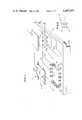
- FIG. 1is an exploded perspective view of a ceramic substrate and two semiconductor chips forming a package according to this invention
- FIG. 2is a sectional view taken substantially along the plane designated by the line 2--2 of FIG. 1;
- FIG. 3is a perspective view of a pedestal according to this invention for attachment to the selected pads on the ceramic substrate;
- FIG. 4is a sectional view similar to FIG. 2 wherein a single chip is connected to the substrate with both flip-chip bonding and wire bonding techniques.
- a conventional ceramic substrate 10is provided for the mounting of semiconductor chips according to this invention.
- the ceramic substrateis configured to mount a flip-chip type chip 12 having conventional Pb/Sn solder balls 14 formed on flip chip face 16 thereof and a wire bond chip 18 having aluminum wires 20 bonded to suitable connections 22 on the face 24 thereof.
- the substrate 10has a first array of Pb/Sn solder pads 26 formed at one location thereon which are arranged to mate with the solder balls 14 on the chip 12. Conventional solder reflow techniques are used to solder the pads 26 to the solder balls 14, and the chip 12 is thus mechanically bonded and electrically connected to the substrate 10.
- This substratealso has a second array of solder pads 28 which are configured to correspond with the outer extremeties of wires 20 on the chip 18.
- a trimetal pedestal 30Connected to each of the pads in the array of pads 28 is a trimetal pedestal 30, one of which is shown in FIG. 3.
- Each pedestal 30has a lower layer of conventional Pb/Sn solder metal 32, an upper layer of aluminum 34, and a central layer of nickel 36 interposed between the solder layer 32 and upper layer 34.
- the layer of solder 32 of each pedestalis solder connected to one of the pads in the array 28 such that an array of pedestals 30 is provided having top surface of aluminum 34 arranged to bond with the wires 20 of the chip 18, and thus, weld connection, such as by ultrasonic welding are made between the aluminum top 34 of the pedestal and the aluminum wires 20 of the chip 18.
- the chip 18also may be adhesively or metallurgically bonded to the surface of the substrate 10, by epoxy or a soldertype alloy 37, for example, if desired.
- Some of the pads of the arrays 26 and 28are interconnected to each other and to metal filled vias 38 by conductors some of which are shown and designated by the reference character 39.
- the viashave brazed thereto input/output pins 40.
- other type pinssuch as swaged pins, could be used, or even non-pin type connections could be used.
- the pedestal 30it is necessary to utilize the pedestal 30 to connect the solder pads 28 to pads suitable for bonding wire bond type chips that typically use aluminum, or sometimes gold wire since neither aluminum nor gold can be effectively bonded to solder.
- aluminum and Pb/Sn solderno appreciable metallurgical bonding action takes place between the two, and in the case of gold and Pb/Sn, the gold is mutually soluble in the solder so that the gold wire can be completely dissolved after a short period of time, thus destroying the connection. Therefore, a separate pedestal for each pad requiring wire bonding is provided.
- the bottom metal 32is solder which will solder bond to the solder pad.
- the intermediate metal 36must bond both to the solder metal 32 and the top metal layer 34, and also act as a barrier between them to prevent migration of the solder metal into the gold or aluminum top metal.
- Nickel or nickel alloysare preferred, but other metals such as copper and copper alloys, and stainless steel, could also be used.
- the top layer 34should be a metal which can be bonded to the wires of the wire bond chip, and these wires are typically aluminum or gold wires.
- the top surface metalshould be aluminum or gold, depending upon the composition of the wire, to provide optimum mono-metallic bonds.
- gold topped pedestalsbe used to bond to gold wire and aluminum topped pedestals be used to bond to aluminum wire since at the elevated temperatures encountered during processing, or reworking, e.g., about 340° C., gold and aluminum rapidly form undesirable intermetallic compounds.
- FIG. 4another embodiment of this invention is also shown which is adapted to provide both wire bond and flip-chip sholder connections to a single chip.
- the substrate 10is provided with an array 26 of solder connections just as previously described which will mate with solder balls 42 on flip-chip semiconductor chip 44.
- the chip 44has an aluminum wire 46 connected to its back side which must be connected to the substrate. This wire can be for any of a number of purposes, such as grounding, etc.
- an additional solder pad 48is provided to which is soldered a pedestal 30.
- the aluminum layer 34 of the pedestalis bonded, e.g., by ultrasonic techniques to the wire 46.
- a substratecan be processed according to conventional techniques to provide solder pad connections, and where these are not appropriate a pedestal 30 can be used to convert the solder pad technology to wire bond technology and both technologies can co-exist on the same substrate.
- a pedestal 30can be used to convert the solder pad technology to wire bond technology and both technologies can co-exist on the same substrate.
- One of the great benefits of this existence of both technologies on the same substrateis that the modules can be processed, and even reworked, by heating to above 340° C. and removing and replacing either a flip-chip or wire bonded chip without adversely affecting the other.
- this techniquecan find application where no flip-chip bonding is utilized at all on some substrates, but only wire bonding is employed.
- Such a techniquecould be employed as a cost saving technique if a manufacturer wants to invest only in one type of technology for substrates, but on some occasions has a need to bond only wire bond type chips to the substrate rather than flip-chip bonding a combination of flip-chip and wire bonding technologies.
- the flip-chip technology type substrate, with solder pads,can then be used to mount only wire bonded chips by utilizing pedestals according to this invention.
Landscapes
- Engineering & Computer Science (AREA)
- Microelectronics & Electronic Packaging (AREA)
- Computer Hardware Design (AREA)
- Power Engineering (AREA)
- Physics & Mathematics (AREA)
- Condensed Matter Physics & Semiconductors (AREA)
- General Physics & Mathematics (AREA)
- Manufacturing & Machinery (AREA)
- Wire Bonding (AREA)
- Electric Connection Of Electric Components To Printed Circuits (AREA)
Abstract
Description
In packaging semiconductor chips, the principal technique is to mount the chips on ceramic or plastic substrates which are used to mount the chips and to provide the necessary pin input/output (I/O) connections. The substrates also may contain some circuit components such as capacitors and resistors. Many times it is desirable to package more than one kind of chip on a given substrate, or to make differnt types of connections to a single chip. Thus mounting pads for each of the chips must be provided as well as the necessary interconnect lines.
There are two principal systems for connecting chips to substrates. One system is the so called flip-chip solder bonding system, wherein solder connections on the face of the chip are soldered to solder pads formed on the substrate. This provides both mechanical bonding and electrical connections between the chip and substrate. The other system is a wire bonding system wherein wires, typically formed of aluminum or gold are connected such as by ultrasonic welding to aluminum, or gold, or other compatible metal on the chips and on the substrate. The chip may also be adhesively bonded to improve mechanical strength. Unfortunately, however, neither aluminium nor gold and solder are compatible, and they cannot be connected to each other, i.e., neither gold wire nor aluminum wire can be bonded to conventional Pb/Sn solder satisfactorily. Thus, it has not been possible to mix the two systems of connections on a single substrate, i.e., the multiple chip substrates have had to be all flip-chip solder bonded or all wire bonded, and any given chip would have only one type of connection.
According to the present invention, a technique is provided where both solder bonding and wire bonding can be performed on the same substrate. To accomplish this an array of solder pads is provided on a substrate. Those pads where wire bonding is to take place each have soldered to them a multi-layered metal pad.Each metal pad has a solder layer soldered to its corresponding pad, an upper layer of metal which will bond to the wire of wire bond chips, and a barrier layer metal interposed between said first two mentioned layers which will bond to each of the said first two mentioned layers, but which is impervious to the solder metal and metal of the top layer. This will convert otherwise wire incompatible solder pads to pads which can be wire bonded. This technique allows any given chip to have both flip chip solder bonds and wire bonds if desired and also any given substrate to have chips of both kinds mounted thereon.
FIG. 1 is an exploded perspective view of a ceramic substrate and two semiconductor chips forming a package according to this invention;
FIG. 2 is a sectional view taken substantially along the plane designated by theline 2--2 of FIG. 1;
FIG. 3 is a perspective view of a pedestal according to this invention for attachment to the selected pads on the ceramic substrate; and
FIG. 4 is a sectional view similar to FIG. 2 wherein a single chip is connected to the substrate with both flip-chip bonding and wire bonding techniques.
Referring now to the drawings, and for the present to FIGS. 1 and 2, a conventionalceramic substrate 10 is provided for the mounting of semiconductor chips according to this invention. The ceramic substrate is configured to mount a flip-chip type chip 12 having conventional Pb/Sn solder balls 14 formed on flip chip face 16 thereof and awire bond chip 18 havingaluminum wires 20 bonded to suitable connections 22 on theface 24 thereof.
Thesubstrate 10 has a first array of Pb/Sn solder pads 26 formed at one location thereon which are arranged to mate with thesolder balls 14 on thechip 12. Conventional solder reflow techniques are used to solder thepads 26 to thesolder balls 14, and thechip 12 is thus mechanically bonded and electrically connected to thesubstrate 10.
This substrate also has a second array ofsolder pads 28 which are configured to correspond with the outer extremeties ofwires 20 on thechip 18. Connected to each of the pads in the array ofpads 28 is atrimetal pedestal 30, one of which is shown in FIG. 3. Eachpedestal 30 has a lower layer of conventional Pb/Sn solder metal 32, an upper layer ofaluminum 34, and a central layer ofnickel 36 interposed between thesolder layer 32 andupper layer 34.
The layer ofsolder 32 of each pedestal is solder connected to one of the pads in thearray 28 such that an array ofpedestals 30 is provided having top surface ofaluminum 34 arranged to bond with thewires 20 of thechip 18, and thus, weld connection, such as by ultrasonic welding are made between thealuminum top 34 of the pedestal and thealuminum wires 20 of thechip 18. Thechip 18 also may be adhesively or metallurgically bonded to the surface of thesubstrate 10, by epoxy or asoldertype alloy 37, for example, if desired.
Some of the pads of thearrays vias 38 by conductors some of which are shown and designated by thereference character 39. The vias have brazed thereto input/output pins 40. Of course, other type pins, such as swaged pins, could be used, or even non-pin type connections could be used.
It is necessary to utilize thepedestal 30 to connect thesolder pads 28 to pads suitable for bonding wire bond type chips that typically use aluminum, or sometimes gold wire since neither aluminum nor gold can be effectively bonded to solder. In the case of aluminum and Pb/Sn solder, no appreciable metallurgical bonding action takes place between the two, and in the case of gold and Pb/Sn, the gold is mutually soluble in the solder so that the gold wire can be completely dissolved after a short period of time, thus destroying the connection. Therefore, a separate pedestal for each pad requiring wire bonding is provided. Thebottom metal 32 is solder which will solder bond to the solder pad. Theintermediate metal 36 must bond both to thesolder metal 32 and thetop metal layer 34, and also act as a barrier between them to prevent migration of the solder metal into the gold or aluminum top metal. Nickel or nickel alloys are preferred, but other metals such as copper and copper alloys, and stainless steel, could also be used.
Thetop layer 34 should be a metal which can be bonded to the wires of the wire bond chip, and these wires are typically aluminum or gold wires. Hence, the top surface metal should be aluminum or gold, depending upon the composition of the wire, to provide optimum mono-metallic bonds.
It is preferred that gold topped pedestals be used to bond to gold wire and aluminum topped pedestals be used to bond to aluminum wire since at the elevated temperatures encountered during processing, or reworking, e.g., about 340° C., gold and aluminum rapidly form undesirable intermetallic compounds.
Referring now to FIG. 4, another embodiment of this invention is also shown which is adapted to provide both wire bond and flip-chip sholder connections to a single chip. In this case thesubstrate 10 is provided with anarray 26 of solder connections just as previously described which will mate withsolder balls 42 on flip-chip semiconductor chip 44. In addition, the chip 44 has analuminum wire 46 connected to its back side which must be connected to the substrate. This wire can be for any of a number of purposes, such as grounding, etc. For such a connection anadditional solder pad 48 is provided to which is soldered apedestal 30. Thealuminum layer 34 of the pedestal is bonded, e.g., by ultrasonic techniques to thewire 46.
By the use of this technique, a substrate can be processed according to conventional techniques to provide solder pad connections, and where these are not appropriate apedestal 30 can be used to convert the solder pad technology to wire bond technology and both technologies can co-exist on the same substrate. One of the great benefits of this existence of both technologies on the same substrate is that the modules can be processed, and even reworked, by heating to above 340° C. and removing and replacing either a flip-chip or wire bonded chip without adversely affecting the other.
Indeed, it is also possible that this technique can find application where no flip-chip bonding is utilized at all on some substrates, but only wire bonding is employed. Such a technique could be employed as a cost saving technique if a manufacturer wants to invest only in one type of technology for substrates, but on some occasions has a need to bond only wire bond type chips to the substrate rather than flip-chip bonding a combination of flip-chip and wire bonding technologies. The flip-chip technology type substrate, with solder pads, can then be used to mount only wire bonded chips by utilizing pedestals according to this invention.
Claims (4)
1. A package for semiconductor integrated circuits comprising:
a substrate having input/output means;
a plurality of solder pads on said substrate;
at least one integrated circuit chip having its back surface attached to said substrate in a face-up configuration with contact pad metal adapted to receive wire bond type connections;
at least one of said solder pads on said substrate having a multi-layer metallic pedestal thereon, said multi-layer metallic pedestal having a solder layer joined to said at least one solder pad, an upper layer of said pedestal made of the same metal as said contact pad metal and adapted to receive wire bond type connections, and a barrier layer of metal interposed between said solder layer and said upper layer, said barrier layer being substantially impervious to both solder and the metal of said upper layer;
a wire formed from the same metal as the contact pad metal and said upper layer, bonded thereto to form a high temperature sustaining wire bond connection between the contact pad metal on the face-up integrated circuit chip and the multi-layer metallic pedestal on the substrate;
a predetermined number of said solder pads arranged in a pattern for interconnecting at least one integrated circuit chip to said substrate in a flip-chip configuration;
at least one integrated circuit chip attached to said substrate in a flip-chip configuration by means of said predetermined number of solder pads which are arranged for interconnecting integrated circuit chips in a flip-chip configuration;
interconnecting conductor lines on said substrate for providing electrical connections between a preselected number of said solder pads which are connecting an integrated circuit chip to said substrate in a face-up configuration and a preselected number of said solder pads connecting an integrated circuit chip to said substrate in a flip-chip configuration.
2. A package for semiconductor integrated circuits as in claim 1 wherein the high temperature sustaining wire bond connection is a mono-metallic system comprising:
an aluminum wire bonded to an aluminum contact pad metal on the face-up integrated circuit chip, and also bonded to an aluminum upper layer of said multi-layer metallic pedestal.
3. A package for semiconductor integrated circuits as in claim 1 wherein the high temperature sustaining connection is a mono-metallic system comprising:
a gold wire bonded to a gold contact pad metal on the face-up integrated circuit chip, and also bonded to a gold upper layer of said multi-layer metallic pedestal.
4. A package for semiconductor integrated circuits as in claim 1 where said barrier layer comprises metal selected from the group consisting of nickel, nickel alloys, copper, copper alloys, and stainless steel.
Priority Applications (4)
| Application Number | Priority Date | Filing Date | Title |
|---|---|---|---|
| US06/328,889US4447857A (en) | 1981-12-09 | 1981-12-09 | Substrate with multiple type connections |
| JP57159722AJPS58101493A (en) | 1981-12-09 | 1982-09-16 | Substrate |
| EP82110816AEP0081135B1 (en) | 1981-12-09 | 1982-11-23 | Substrate for mounting integrated circuit chips |
| DE8282110816TDE3275789D1 (en) | 1981-12-09 | 1982-11-23 | Substrate for mounting integrated circuit chips |
Applications Claiming Priority (1)
| Application Number | Priority Date | Filing Date | Title |
|---|---|---|---|
| US06/328,889US4447857A (en) | 1981-12-09 | 1981-12-09 | Substrate with multiple type connections |
Publications (1)
| Publication Number | Publication Date |
|---|---|
| US4447857Atrue US4447857A (en) | 1984-05-08 |
Family
ID=23282896
Family Applications (1)
| Application Number | Title | Priority Date | Filing Date |
|---|---|---|---|
| US06/328,889Expired - LifetimeUS4447857A (en) | 1981-12-09 | 1981-12-09 | Substrate with multiple type connections |
Country Status (4)
| Country | Link |
|---|---|
| US (1) | US4447857A (en) |
| EP (1) | EP0081135B1 (en) |
| JP (1) | JPS58101493A (en) |
| DE (1) | DE3275789D1 (en) |
Cited By (42)
| Publication number | Priority date | Publication date | Assignee | Title |
|---|---|---|---|---|
| US4558346A (en)* | 1982-03-29 | 1985-12-10 | Fujitsu Limited | Highly reliable hermetically sealed package for a semiconductor device |
| US4706166A (en)* | 1986-04-25 | 1987-11-10 | Irvine Sensors Corporation | High-density electronic modules--process and product |
| US4783722A (en)* | 1985-07-16 | 1988-11-08 | Nippon Telegraph And Telephone Corporation | Interboard connection terminal and method of manufacturing the same |
| US4837928A (en)* | 1986-10-17 | 1989-06-13 | Cominco Ltd. | Method of producing a jumper chip for semiconductor devices |
| US4860443A (en)* | 1987-01-21 | 1989-08-29 | Hughes Aircraft Company | Method for connecting leadless chip package |
| US4873615A (en)* | 1986-10-09 | 1989-10-10 | Amp Incorporated | Semiconductor chip carrier system |
| US4955523A (en)* | 1986-12-17 | 1990-09-11 | Raychem Corporation | Interconnection of electronic components |
| US5189507A (en)* | 1986-12-17 | 1993-02-23 | Raychem Corporation | Interconnection of electronic components |
| US5252882A (en)* | 1990-07-02 | 1993-10-12 | Japan Radio Co., Ltd. | Surface acoustic wave device and its manufacturing method |
| US5274531A (en)* | 1991-06-17 | 1993-12-28 | The Intec Group, Inc. | Lead frame with aluminum rivets |
| WO1994001987A1 (en)* | 1992-07-06 | 1994-01-20 | Telefonaktiebolaget Lm Ericsson | Component module |
| US5400221A (en)* | 1992-10-21 | 1995-03-21 | Nec Corporation | Printed circuit board mounted with electric elements thereon |
| US5455390A (en)* | 1994-02-01 | 1995-10-03 | Tessera, Inc. | Microelectronics unit mounting with multiple lead bonding |
| US5518964A (en)* | 1994-07-07 | 1996-05-21 | Tessera, Inc. | Microelectronic mounting with multiple lead deformation and bonding |
| US5688716A (en)* | 1994-07-07 | 1997-11-18 | Tessera, Inc. | Fan-out semiconductor chip assembly |
| US5696031A (en)* | 1996-11-20 | 1997-12-09 | Micron Technology, Inc. | Device and method for stacking wire-bonded integrated circuit dice on flip-chip bonded integrated circuit dice |
| US5798286A (en)* | 1995-09-22 | 1998-08-25 | Tessera, Inc. | Connecting multiple microelectronic elements with lead deformation |
| US5820014A (en) | 1993-11-16 | 1998-10-13 | Form Factor, Inc. | Solder preforms |
| US5830782A (en)* | 1994-07-07 | 1998-11-03 | Tessera, Inc. | Microelectronic element bonding with deformation of leads in rows |
| US5844317A (en)* | 1995-12-21 | 1998-12-01 | International Business Machines Corporation | Consolidated chip design for wire bond and flip-chip package technologies |
| US5907769A (en)* | 1996-12-30 | 1999-05-25 | Micron Technology, Inc. | Leads under chip in conventional IC package |
| US5994152A (en) | 1996-02-21 | 1999-11-30 | Formfactor, Inc. | Fabricating interconnects and tips using sacrificial substrates |
| US6117694A (en)* | 1994-07-07 | 2000-09-12 | Tessera, Inc. | Flexible lead structures and methods of making same |
| US6133072A (en)* | 1996-12-13 | 2000-10-17 | Tessera, Inc. | Microelectronic connector with planar elastomer sockets |
| US6204074B1 (en) | 1995-01-09 | 2001-03-20 | International Business Machines Corporation | Chip design process for wire bond and flip-chip package |
| US6274823B1 (en) | 1993-11-16 | 2001-08-14 | Formfactor, Inc. | Interconnection substrates with resilient contact structures on both sides |
| US6373143B1 (en) | 1998-09-24 | 2002-04-16 | International Business Machines Corporation | Integrated circuit having wirebond pads suitable for probing |
| US20020045290A1 (en)* | 1996-02-20 | 2002-04-18 | Michael B. Ball | Flip chip and conventional stack |
| US6429112B1 (en) | 1994-07-07 | 2002-08-06 | Tessera, Inc. | Multi-layer substrates and fabrication processes |
| US20030071346A1 (en)* | 1994-07-07 | 2003-04-17 | Tessera, Inc. | Flexible lead structures and methods of making same |
| US6611434B1 (en)* | 2000-10-30 | 2003-08-26 | Siliconware Precision Industries Co., Ltd. | Stacked multi-chip package structure with on-chip integration of passive component |
| US20030197199A1 (en)* | 2000-01-31 | 2003-10-23 | Noriaki Sakamoto | Semiconductor device and semiconductor module |
| EP1122782A3 (en)* | 2000-01-31 | 2004-01-02 | Visteon Global Technologies, Inc. | Etched tri-layer metal with integrated wire traces for wire bonding |
| US20040169277A1 (en)* | 1998-07-01 | 2004-09-02 | Fujitsu Limted | Multileveled printed circuit board unit including substrate interposed between stacked bumps |
| US20050155223A1 (en)* | 1994-07-07 | 2005-07-21 | Tessera, Inc. | Methods of making microelectronic assemblies |
| US20060049529A1 (en)* | 2004-09-03 | 2006-03-09 | Honeywell International, Inc. | Flip chip metal bonding to plastic leadframe |
| US7220921B1 (en)* | 2000-05-09 | 2007-05-22 | Sanyo Electric Co., Ltd. | Sheet-like board member and method of manufacturing a semiconductor device |
| US7601039B2 (en) | 1993-11-16 | 2009-10-13 | Formfactor, Inc. | Microelectronic contact structure and method of making same |
| US8033838B2 (en) | 1996-02-21 | 2011-10-11 | Formfactor, Inc. | Microelectronic contact structure |
| US8373428B2 (en) | 1993-11-16 | 2013-02-12 | Formfactor, Inc. | Probe card assembly and kit, and methods of making same |
| US9269681B2 (en) | 2012-11-16 | 2016-02-23 | Qualcomm Incorporated | Surface finish on trace for a thermal compression flip chip (TCFC) |
| US11239158B1 (en)* | 2020-10-08 | 2022-02-01 | Qualcomm Incorporated | Wire bond inductor structures for flip chip dies |
Families Citing this family (7)
| Publication number | Priority date | Publication date | Assignee | Title |
|---|---|---|---|---|
| JPS61296800A (en)* | 1985-06-25 | 1986-12-27 | 日本電気株式会社 | Electrode for altering design |
| DE3704200A1 (en)* | 1987-02-11 | 1988-08-25 | Bbc Brown Boveri & Cie | METHOD FOR PRODUCING A CONNECTION BETWEEN A BONDED WIRE AND A CONTACT AREA IN HYBRID THICK-LAYER CIRCUITS |
| JPS63158863U (en)* | 1987-04-07 | 1988-10-18 | ||
| DE3817600C2 (en)* | 1987-05-26 | 1994-06-23 | Matsushita Electric Works Ltd | Method of manufacturing a semiconductor device with a ceramic substrate and an integrated circuit |
| GB2356490B (en)* | 1996-08-27 | 2001-08-15 | Nec Corp | A multi-chip module mountable on a printed circuit board |
| US5969417A (en)* | 1996-08-27 | 1999-10-19 | Nec Corporation | Chip package device mountable on a mother board in whichever of facedown and wire bonding manners |
| US8125060B2 (en) | 2006-12-08 | 2012-02-28 | Infineon Technologies Ag | Electronic component with layered frame |
Citations (8)
| Publication number | Priority date | Publication date | Assignee | Title |
|---|---|---|---|---|
| US3544704A (en)* | 1969-01-21 | 1970-12-01 | Motorola Inc | Bonding islands for hybrid circuits |
| US3591839A (en)* | 1969-08-27 | 1971-07-06 | Siliconix Inc | Micro-electronic circuit with novel hermetic sealing structure and method of manufacture |
| US3770874A (en)* | 1970-09-08 | 1973-11-06 | Siemens Ag | Contact members for soldering electrical components |
| US3778530A (en)* | 1971-04-01 | 1973-12-11 | W Reimann | Flatpack lead positioning device |
| US3781596A (en)* | 1972-07-07 | 1973-12-25 | R Galli | Semiconductor chip carriers and strips thereof |
| US3809797A (en)* | 1971-11-16 | 1974-05-07 | Du Pont | Seal ring compositions and electronic packages made therewith |
| US4074342A (en)* | 1974-12-20 | 1978-02-14 | International Business Machines Corporation | Electrical package for lsi devices and assembly process therefor |
| US4145120A (en)* | 1975-09-19 | 1979-03-20 | Kabushiki Kaisha Suwa Seikosha | Electronic table calculator using liquid crystal display |
Family Cites Families (3)
| Publication number | Priority date | Publication date | Assignee | Title |
|---|---|---|---|---|
| US3554821A (en)* | 1967-07-17 | 1971-01-12 | Rca Corp | Process for manufacturing microminiature electrical component mounting assemblies |
| DE2032872B2 (en)* | 1970-07-02 | 1975-03-20 | Siemens Ag, 1000 Berlin Und 8000 Muenchen | Process for the production of soft solderable contacts for the installation of semiconductor components in housings |
| US4179802A (en)* | 1978-03-27 | 1979-12-25 | International Business Machines Corporation | Studded chip attachment process |
- 1981
- 1981-12-09USUS06/328,889patent/US4447857A/ennot_activeExpired - Lifetime
- 1982
- 1982-09-16JPJP57159722Apatent/JPS58101493A/enactiveGranted
- 1982-11-23EPEP82110816Apatent/EP0081135B1/ennot_activeExpired
- 1982-11-23DEDE8282110816Tpatent/DE3275789D1/ennot_activeExpired
Patent Citations (8)
| Publication number | Priority date | Publication date | Assignee | Title |
|---|---|---|---|---|
| US3544704A (en)* | 1969-01-21 | 1970-12-01 | Motorola Inc | Bonding islands for hybrid circuits |
| US3591839A (en)* | 1969-08-27 | 1971-07-06 | Siliconix Inc | Micro-electronic circuit with novel hermetic sealing structure and method of manufacture |
| US3770874A (en)* | 1970-09-08 | 1973-11-06 | Siemens Ag | Contact members for soldering electrical components |
| US3778530A (en)* | 1971-04-01 | 1973-12-11 | W Reimann | Flatpack lead positioning device |
| US3809797A (en)* | 1971-11-16 | 1974-05-07 | Du Pont | Seal ring compositions and electronic packages made therewith |
| US3781596A (en)* | 1972-07-07 | 1973-12-25 | R Galli | Semiconductor chip carriers and strips thereof |
| US4074342A (en)* | 1974-12-20 | 1978-02-14 | International Business Machines Corporation | Electrical package for lsi devices and assembly process therefor |
| US4145120A (en)* | 1975-09-19 | 1979-03-20 | Kabushiki Kaisha Suwa Seikosha | Electronic table calculator using liquid crystal display |
Non-Patent Citations (4)
| Title |
|---|
| F. W. Eurglunes, Via Hole Filling Technique, IBM Tech. Disc. Bull., vol. 12, #4, Sep. 1969, p. 596. |
| F. W. Eurglunes, Via Hole Filling Technique, IBM Tech. Disc. Bull., vol. 12, 4, Sep. 1969, p. 596.* |
| Gedney et al., Low Cost Integrated Circuit, IBM Tech. Disc. Bull., vol. 20, 9, Feb. 1978, pp. 3399 & 3400.* |
| Gedney et al., Low-Cost Integrated Circuit, IBM Tech. Disc. Bull., vol. 20, #9, Feb. 1978, pp. 3399 & 3400. |
Cited By (101)
| Publication number | Priority date | Publication date | Assignee | Title |
|---|---|---|---|---|
| US4558346A (en)* | 1982-03-29 | 1985-12-10 | Fujitsu Limited | Highly reliable hermetically sealed package for a semiconductor device |
| US4783722A (en)* | 1985-07-16 | 1988-11-08 | Nippon Telegraph And Telephone Corporation | Interboard connection terminal and method of manufacturing the same |
| US4897918A (en)* | 1985-07-16 | 1990-02-06 | Nippon Telegraph And Telephone | Method of manufacturing an interboard connection terminal |
| US4706166A (en)* | 1986-04-25 | 1987-11-10 | Irvine Sensors Corporation | High-density electronic modules--process and product |
| US4873615A (en)* | 1986-10-09 | 1989-10-10 | Amp Incorporated | Semiconductor chip carrier system |
| US4837928A (en)* | 1986-10-17 | 1989-06-13 | Cominco Ltd. | Method of producing a jumper chip for semiconductor devices |
| US4955523A (en)* | 1986-12-17 | 1990-09-11 | Raychem Corporation | Interconnection of electronic components |
| US5189507A (en)* | 1986-12-17 | 1993-02-23 | Raychem Corporation | Interconnection of electronic components |
| US4860443A (en)* | 1987-01-21 | 1989-08-29 | Hughes Aircraft Company | Method for connecting leadless chip package |
| US5252882A (en)* | 1990-07-02 | 1993-10-12 | Japan Radio Co., Ltd. | Surface acoustic wave device and its manufacturing method |
| US5274531A (en)* | 1991-06-17 | 1993-12-28 | The Intec Group, Inc. | Lead frame with aluminum rivets |
| WO1994001987A1 (en)* | 1992-07-06 | 1994-01-20 | Telefonaktiebolaget Lm Ericsson | Component module |
| US5400221A (en)* | 1992-10-21 | 1995-03-21 | Nec Corporation | Printed circuit board mounted with electric elements thereon |
| AU672433B2 (en)* | 1992-10-21 | 1996-10-03 | Nec Corporation | A printed circuit board mounted with electric elements thereon |
| US6274823B1 (en) | 1993-11-16 | 2001-08-14 | Formfactor, Inc. | Interconnection substrates with resilient contact structures on both sides |
| US5820014A (en) | 1993-11-16 | 1998-10-13 | Form Factor, Inc. | Solder preforms |
| US8373428B2 (en) | 1993-11-16 | 2013-02-12 | Formfactor, Inc. | Probe card assembly and kit, and methods of making same |
| US7601039B2 (en) | 1993-11-16 | 2009-10-13 | Formfactor, Inc. | Microelectronic contact structure and method of making same |
| US5455390A (en)* | 1994-02-01 | 1995-10-03 | Tessera, Inc. | Microelectronics unit mounting with multiple lead bonding |
| US5794330A (en)* | 1994-02-01 | 1998-08-18 | Tessera, Inc. | Microelectronics unit mounting with multiple lead bonding |
| US5801441A (en)* | 1994-07-07 | 1998-09-01 | Tessera, Inc. | Microelectronic mounting with multiple lead deformation and bonding |
| US6104087A (en)* | 1994-07-07 | 2000-08-15 | Tessera, Inc. | Microelectronic assemblies with multiple leads |
| US5830782A (en)* | 1994-07-07 | 1998-11-03 | Tessera, Inc. | Microelectronic element bonding with deformation of leads in rows |
| US5518964A (en)* | 1994-07-07 | 1996-05-21 | Tessera, Inc. | Microelectronic mounting with multiple lead deformation and bonding |
| US6429112B1 (en) | 1994-07-07 | 2002-08-06 | Tessera, Inc. | Multi-layer substrates and fabrication processes |
| US5913109A (en)* | 1994-07-07 | 1999-06-15 | Tessera, Inc. | Fixtures and methods for lead bonding and deformation |
| US5959354A (en)* | 1994-07-07 | 1999-09-28 | Tessera, Inc. | Connection components with rows of lead bond sections |
| US5688716A (en)* | 1994-07-07 | 1997-11-18 | Tessera, Inc. | Fan-out semiconductor chip assembly |
| US7166914B2 (en) | 1994-07-07 | 2007-01-23 | Tessera, Inc. | Semiconductor package with heat sink |
| US20050155223A1 (en)* | 1994-07-07 | 2005-07-21 | Tessera, Inc. | Methods of making microelectronic assemblies |
| US6080603A (en)* | 1994-07-07 | 2000-06-27 | Tessera, Inc. | Fixtures and methods for lead bonding and deformation |
| US6265765B1 (en) | 1994-07-07 | 2001-07-24 | Tessera, Inc. | Fan-out semiconductor chip assembly |
| US6117694A (en)* | 1994-07-07 | 2000-09-12 | Tessera, Inc. | Flexible lead structures and methods of making same |
| US6828668B2 (en) | 1994-07-07 | 2004-12-07 | Tessera, Inc. | Flexible lead structures and methods of making same |
| US6635553B1 (en) | 1994-07-07 | 2003-10-21 | Iessera, Inc. | Microelectronic assemblies with multiple leads |
| US20030071346A1 (en)* | 1994-07-07 | 2003-04-17 | Tessera, Inc. | Flexible lead structures and methods of making same |
| US6194291B1 (en) | 1994-07-07 | 2001-02-27 | Tessera, Inc. | Microelectronic assemblies with multiple leads |
| US6204074B1 (en) | 1995-01-09 | 2001-03-20 | International Business Machines Corporation | Chip design process for wire bond and flip-chip package |
| US6147400A (en)* | 1995-09-22 | 2000-11-14 | Tessera, Inc. | Connecting multiple microelectronic elements with lead deformation |
| US6365436B1 (en) | 1995-09-22 | 2002-04-02 | Tessera, Inc. | Connecting multiple microelectronic elements with lead deformation |
| US5798286A (en)* | 1995-09-22 | 1998-08-25 | Tessera, Inc. | Connecting multiple microelectronic elements with lead deformation |
| US5844317A (en)* | 1995-12-21 | 1998-12-01 | International Business Machines Corporation | Consolidated chip design for wire bond and flip-chip package technologies |
| US7166495B2 (en) | 1996-02-20 | 2007-01-23 | Micron Technology, Inc. | Method of fabricating a multi-die semiconductor package assembly |
| US6140149A (en)* | 1996-02-20 | 2000-10-31 | Micron Technology, Inc. | Device and method for stacking wire-bonded integrated circuit dice on flip-chip bonded integrated circuit dice |
| US20070117266A1 (en)* | 1996-02-20 | 2007-05-24 | Ball Michael B | Method of fabricating a multi-die semiconductor package assembly |
| US20020045290A1 (en)* | 1996-02-20 | 2002-04-18 | Michael B. Ball | Flip chip and conventional stack |
| US8033838B2 (en) | 1996-02-21 | 2011-10-11 | Formfactor, Inc. | Microelectronic contact structure |
| US5994152A (en) | 1996-02-21 | 1999-11-30 | Formfactor, Inc. | Fabricating interconnects and tips using sacrificial substrates |
| US7423338B2 (en) | 1996-11-20 | 2008-09-09 | Micron Technology, Inc. | Methods for stacking wire-bonded integrated circuit dice on flip-chip bonded integrated circuit dice |
| US7282792B2 (en) | 1996-11-20 | 2007-10-16 | Micron Technology, Inc. | Methods for stacking wire-bonded integrated circuit dice on flip-chip bonded integrated circuit dice |
| US20080315435A1 (en)* | 1996-11-20 | 2008-12-25 | Micron Technology, Inc. | Methods for stacking wire-bonded integrated circuit dice on flip-chip bonded integrated circuit dice |
| US7109059B2 (en) | 1996-11-20 | 2006-09-19 | Micron Technology, Inc. | Methods for stacking wire-bonded integrated circuit dice on flip-chip bonded integrated circuit dice |
| US20080311702A1 (en)* | 1996-11-20 | 2008-12-18 | Micron Technology, Inc. | Methods for stacking wire-bonded integrated circuit dice on flip-chip bonded integrated circuit dice |
| US7812436B2 (en) | 1996-11-20 | 2010-10-12 | Micron Technology, Inc. | Methods for stacking wire-bonded integrated circuit dice on flip-chip bonded integrated circuit dice |
| US6605489B2 (en) | 1996-11-20 | 2003-08-12 | Micron Technology, Inc. | Methods for stacking wire-bonded integrated circuit dice on flip-chip bonded integrated circuit dice |
| US7423339B2 (en) | 1996-11-20 | 2008-09-09 | Mircon Technology, Inc. | Methods for stacking wire-bonded integrated circuit dice on flip-chip bonded integrated circuit dice |
| US5973403A (en)* | 1996-11-20 | 1999-10-26 | Micron Technology, Inc. | Device and method for stacking wire-bonded integrated circuit dice on flip-chip bonded integrated circuit dice |
| US6399416B1 (en) | 1996-11-20 | 2002-06-04 | Micron Technology, Inc. | Device and method for stacking wire-bonded integrated circuit dice on flip-chip bonded integrated circuit dice |
| US7411286B2 (en) | 1996-11-20 | 2008-08-12 | Micron Technology, Inc. | Methods for stacking wire-bonded integrated circuit dice on flip-chip bonded integrated circuit dice |
| US20040029315A1 (en)* | 1996-11-20 | 2004-02-12 | Wark James M. | Methods for stacking wire-bonded integrated circuit dice on flip-chip bonded integrated circuit dice |
| US7402902B2 (en) | 1996-11-20 | 2008-07-22 | Micron Technology, Inc. | Methods for stacking wire-bonded integrated circuit dice on flip-chip bonded integrated circuit dice |
| US7776652B2 (en) | 1996-11-20 | 2010-08-17 | Micron Technology, Inc. | Methods for stacking wire-bonded integrated circuit dice on flip-chip bonded integrated circuit dice |
| US5696031A (en)* | 1996-11-20 | 1997-12-09 | Micron Technology, Inc. | Device and method for stacking wire-bonded integrated circuit dice on flip-chip bonded integrated circuit dice |
| US6869826B2 (en) | 1996-11-20 | 2005-03-22 | Micron Technology, Inc. | Methods for stacking wire-bonded integrated circuit dice on flip-chip bonded integrated circuit dice |
| US20070063326A1 (en)* | 1996-11-20 | 2007-03-22 | Wark James M | Methods for stacking wire-bonded integrated circuit dice on flip-chip bonded integrated circuit dice |
| US6071754A (en)* | 1996-11-20 | 2000-06-06 | Micron Technology, Inc. | Device and method for stacking wire-bonded integrated circuit dice on flip-chip bonded integrated circuit dice |
| US20050161796A1 (en)* | 1996-11-20 | 2005-07-28 | Wark James M. | Methods for stacking wire-bonded integrated circuit dice on flip-chip bonded integrated circuit dice |
| US20070063328A1 (en)* | 1996-11-20 | 2007-03-22 | Wark James M | Methods for stacking wire-bonded integrated circuit dice on flip-chip bonded integrated circuit dice |
| US20070063229A1 (en)* | 1996-11-20 | 2007-03-22 | Wark James M | Methods for stacking wire-bonded integrated circuit dice on flip-chip bonded integrated circuit dice |
| US20060033194A1 (en)* | 1996-11-20 | 2006-02-16 | Wark James M | Methods for stacking wire-bonded integrated circuit dice on flip-chip bonded integrated circuit dice |
| US20070063327A1 (en)* | 1996-11-20 | 2007-03-22 | Wark James M | Methods for stacking wire-bonded integrated circuit dice on flip-chip bonded integrated circuit dice |
| US6133072A (en)* | 1996-12-13 | 2000-10-17 | Tessera, Inc. | Microelectronic connector with planar elastomer sockets |
| US6541867B1 (en) | 1996-12-13 | 2003-04-01 | Tessera, Inc. | Microelectronic connector with planar elastomer sockets |
| US7084490B2 (en) | 1996-12-30 | 2006-08-01 | Micron Technology, Inc. | Leads under chip IC package |
| US6830961B2 (en) | 1996-12-30 | 2004-12-14 | Micron Technology, Inc. | Methods for leads under chip in conventional IC package |
| US20010045629A1 (en)* | 1996-12-30 | 2001-11-29 | Corisis David J. | Leads under chip in conventional IC package |
| US6277673B1 (en) | 1996-12-30 | 2001-08-21 | Micron Technology, Inc. | Leads under chip in conventional IC package |
| US20030067059A1 (en)* | 1996-12-30 | 2003-04-10 | Corisis David J. | Leads under chip in conventional IC package |
| US20050248006A1 (en)* | 1996-12-30 | 2005-11-10 | Corisis David J | Leads under chip IC package |
| US6958528B2 (en) | 1996-12-30 | 2005-10-25 | Micron Technology, Inc. | Leads under chip IC package |
| US5907769A (en)* | 1996-12-30 | 1999-05-25 | Micron Technology, Inc. | Leads under chip in conventional IC package |
| US6271580B1 (en) | 1996-12-30 | 2001-08-07 | Micron Technology, Inc. | Leads under chip in conventional IC package |
| US6445061B2 (en) | 1996-12-30 | 2002-09-03 | Micron Technology, Inc. | Leads under chip in conventional IC package |
| US6130474A (en)* | 1996-12-30 | 2000-10-10 | Micron Technology, Inc. | Leads under chip IC package |
| US20040169277A1 (en)* | 1998-07-01 | 2004-09-02 | Fujitsu Limted | Multileveled printed circuit board unit including substrate interposed between stacked bumps |
| US20090178835A1 (en)* | 1998-07-01 | 2009-07-16 | Fujitsu Limited | Multileveled printed circuit board unit including substrate interposed between stacked bumps |
| US7489518B2 (en)* | 1998-07-01 | 2009-02-10 | Fujitsu Limited | Multileveled printed circuit board unit including substrate interposed between stacked bumps |
| US8089775B2 (en) | 1998-07-01 | 2012-01-03 | Fujitsu Limited | Multileveled printed circuit board unit including substrate interposed between stacked bumps |
| US6429675B2 (en) | 1998-09-24 | 2002-08-06 | International Business Machines Corporation | Structure and method for probing wiring bond pads |
| US6373143B1 (en) | 1998-09-24 | 2002-04-16 | International Business Machines Corporation | Integrated circuit having wirebond pads suitable for probing |
| US20050146052A1 (en)* | 2000-01-31 | 2005-07-07 | Sanyo Electric Co., Ltd., An Osaka, Japan Corporation | Semiconductor device and semiconductor module |
| US20030197199A1 (en)* | 2000-01-31 | 2003-10-23 | Noriaki Sakamoto | Semiconductor device and semiconductor module |
| EP1122782A3 (en)* | 2000-01-31 | 2004-01-02 | Visteon Global Technologies, Inc. | Etched tri-layer metal with integrated wire traces for wire bonding |
| US7276793B2 (en) | 2000-01-31 | 2007-10-02 | Sanyo Electric Co., Ltd. | Semiconductor device and semiconductor module |
| US7173336B2 (en) | 2000-01-31 | 2007-02-06 | Sanyo Electric Co., Ltd. | Hybrid integrated circuit device |
| US7220921B1 (en)* | 2000-05-09 | 2007-05-22 | Sanyo Electric Co., Ltd. | Sheet-like board member and method of manufacturing a semiconductor device |
| US6611434B1 (en)* | 2000-10-30 | 2003-08-26 | Siliconware Precision Industries Co., Ltd. | Stacked multi-chip package structure with on-chip integration of passive component |
| US7112873B2 (en)* | 2004-09-03 | 2006-09-26 | Honeywell International Inc. | Flip chip metal bonding to plastic leadframe |
| US20060049529A1 (en)* | 2004-09-03 | 2006-03-09 | Honeywell International, Inc. | Flip chip metal bonding to plastic leadframe |
| US9269681B2 (en) | 2012-11-16 | 2016-02-23 | Qualcomm Incorporated | Surface finish on trace for a thermal compression flip chip (TCFC) |
| US11239158B1 (en)* | 2020-10-08 | 2022-02-01 | Qualcomm Incorporated | Wire bond inductor structures for flip chip dies |
Also Published As
| Publication number | Publication date |
|---|---|
| JPS58101493A (en) | 1983-06-16 |
| DE3275789D1 (en) | 1987-04-23 |
| EP0081135A2 (en) | 1983-06-15 |
| EP0081135A3 (en) | 1984-07-25 |
| EP0081135B1 (en) | 1987-03-18 |
| JPS6352776B2 (en) | 1988-10-20 |
Similar Documents
| Publication | Publication Date | Title |
|---|---|---|
| US4447857A (en) | Substrate with multiple type connections | |
| US6303992B1 (en) | Interposer for mounting semiconductor dice on substrates | |
| EP0097833B1 (en) | Substrate for integrated circuit packages | |
| US5477082A (en) | Bi-planar multi-chip module | |
| US5942795A (en) | Leaded substrate carrier for integrated circuit device and leaded substrate carrier device assembly | |
| US6082610A (en) | Method of forming interconnections on electronic modules | |
| US6180265B1 (en) | Flip chip solder bump pad | |
| US5796591A (en) | Direct chip attach circuit card | |
| US5438224A (en) | Integrated circuit package having a face-to-face IC chip arrangement | |
| US5066614A (en) | Method of manufacturing a leadframe having conductive elements preformed with solder bumps | |
| US5715144A (en) | Multi-layer, multi-chip pyramid and circuit board structure | |
| US6847118B2 (en) | Low temperature solder chip attach structure | |
| US5897341A (en) | Diffusion bonded interconnect | |
| US6333563B1 (en) | Electrical interconnection package and method thereof | |
| GB2117564A (en) | Mounting one integrated circuit upon another | |
| US4898320A (en) | Method of manufacturing a high-yield solder bumped semiconductor wafer | |
| US5808875A (en) | Integrated circuit solder-rack interconnect module | |
| US4892245A (en) | Controlled compression furnace bonding | |
| US5770477A (en) | Flip chip-on-flip chip multi-chip module | |
| US5099306A (en) | Stacked tab leadframe assembly | |
| JPH08153834A (en) | Mcm carrier | |
| US7923125B2 (en) | Apparatus for solder crack deflection | |
| US4980753A (en) | Low-cost high-performance semiconductor chip package | |
| US20050116322A1 (en) | Circuit module | |
| KR20080024217A (en) | Lead Free Semiconductor Packages |
Legal Events
| Date | Code | Title | Description |
|---|---|---|---|
| AS | Assignment | Owner name:INTERNATIONAL BUSINESS MACHINES CORPORATION, ARMON Free format text:ASSIGNMENT OF ASSIGNORS INTEREST.;ASSIGNORS:MARKS, ROBERT;PHELPS, DOUGLAS W. JR.;WARD, WILLIAM C.;REEL/FRAME:003957/0481 Effective date:19811207 | |
| STCF | Information on status: patent grant | Free format text:PATENTED CASE | |
| FPAY | Fee payment | Year of fee payment:4 | |
| FPAY | Fee payment | Year of fee payment:8 | |
| FPAY | Fee payment | Year of fee payment:12 |