US4444616A - Method for exposure of chemically machinable light-sensitive glass - Google Patents
Method for exposure of chemically machinable light-sensitive glassDownload PDFInfo
- Publication number
- US4444616A US4444616AUS06/384,111US38411182AUS4444616AUS 4444616 AUS4444616 AUS 4444616AUS 38411182 AUS38411182 AUS 38411182AUS 4444616 AUS4444616 AUS 4444616A
- Authority
- US
- United States
- Prior art keywords
- glass plate
- ultraviolet rays
- light
- parallel bundle
- parallel
- Prior art date
- Legal status (The legal status is an assumption and is not a legal conclusion. Google has not performed a legal analysis and makes no representation as to the accuracy of the status listed.)
- Expired - Fee Related
Links
- 239000011521glassSubstances0.000titleclaimsabstractdescription69
- 238000000034methodMethods0.000titleclaimsabstractdescription20
- 230000001678irradiating effectEffects0.000claimsabstractdescription7
- KRHYYFGTRYWZRS-UHFFFAOYSA-NFluoraneChemical compoundFKRHYYFGTRYWZRS-UHFFFAOYSA-N0.000claimsdescription14
- 239000013078crystalSubstances0.000claimsdescription4
- PAZHGORSDKKUPI-UHFFFAOYSA-Nlithium metasilicateChemical compound[Li+].[Li+].[O-][Si]([O-])=OPAZHGORSDKKUPI-UHFFFAOYSA-N0.000claimsdescription3
- 229910052912lithium silicateInorganic materials0.000claimsdescription3
- 238000010438heat treatmentMethods0.000claims2
- 238000007796conventional methodMethods0.000description5
- 238000005530etchingMethods0.000description3
- VYPSYNLAJGMNEJ-UHFFFAOYSA-NSilicium dioxideChemical compoundO=[Si]=OVYPSYNLAJGMNEJ-UHFFFAOYSA-N0.000description2
- 230000001154acute effectEffects0.000description2
- 229910011763Li2 OInorganic materials0.000description1
- 239000002253acidSubstances0.000description1
- 230000015572biosynthetic processEffects0.000description1
- 229910052681coesiteInorganic materials0.000description1
- 229910052906cristobaliteInorganic materials0.000description1
- 238000005520cutting processMethods0.000description1
- 238000007496glass formingMethods0.000description1
- 238000002360preparation methodMethods0.000description1
- 239000000377silicon dioxideSubstances0.000description1
- 229910052682stishoviteInorganic materials0.000description1
- 229910052905tridymiteInorganic materials0.000description1
Images
Classifications
- H—ELECTRICITY
- H01—ELECTRIC ELEMENTS
- H01J—ELECTRIC DISCHARGE TUBES OR DISCHARGE LAMPS
- H01J17/00—Gas-filled discharge tubes with solid cathode
- H01J17/38—Cold-cathode tubes
- H01J17/48—Cold-cathode tubes with more than one cathode or anode, e.g. sequence-discharge tube, counting tube, dekatron
- H01J17/49—Display panels, e.g. with crossed electrodes, e.g. making use of direct current
- C—CHEMISTRY; METALLURGY
- C03—GLASS; MINERAL OR SLAG WOOL
- C03C—CHEMICAL COMPOSITION OF GLASSES, GLAZES OR VITREOUS ENAMELS; SURFACE TREATMENT OF GLASS; SURFACE TREATMENT OF FIBRES OR FILAMENTS MADE FROM GLASS, MINERALS OR SLAGS; JOINING GLASS TO GLASS OR OTHER MATERIALS
- C03C15/00—Surface treatment of glass, not in the form of fibres or filaments, by etching
- C—CHEMISTRY; METALLURGY
- C03—GLASS; MINERAL OR SLAG WOOL
- C03C—CHEMICAL COMPOSITION OF GLASSES, GLAZES OR VITREOUS ENAMELS; SURFACE TREATMENT OF GLASS; SURFACE TREATMENT OF FIBRES OR FILAMENTS MADE FROM GLASS, MINERALS OR SLAGS; JOINING GLASS TO GLASS OR OTHER MATERIALS
- C03C23/00—Other surface treatment of glass not in the form of fibres or filaments
- C03C23/0005—Other surface treatment of glass not in the form of fibres or filaments by irradiation
- C03C23/002—Other surface treatment of glass not in the form of fibres or filaments by irradiation by ultraviolet light
- G—PHYSICS
- G03—PHOTOGRAPHY; CINEMATOGRAPHY; ANALOGOUS TECHNIQUES USING WAVES OTHER THAN OPTICAL WAVES; ELECTROGRAPHY; HOLOGRAPHY
- G03F—PHOTOMECHANICAL PRODUCTION OF TEXTURED OR PATTERNED SURFACES, e.g. FOR PRINTING, FOR PROCESSING OF SEMICONDUCTOR DEVICES; MATERIALS THEREFOR; ORIGINALS THEREFOR; APPARATUS SPECIALLY ADAPTED THEREFOR
- G03F7/00—Photomechanical, e.g. photolithographic, production of textured or patterned surfaces, e.g. printing surfaces; Materials therefor, e.g. comprising photoresists; Apparatus specially adapted therefor
- G03F7/20—Exposure; Apparatus therefor
- G03F7/2002—Exposure; Apparatus therefor with visible light or UV light, through an original having an opaque pattern on a transparent support, e.g. film printing, projection printing; by reflection of visible or UV light from an original such as a printed image
- G03F7/201—Exposure; Apparatus therefor with visible light or UV light, through an original having an opaque pattern on a transparent support, e.g. film printing, projection printing; by reflection of visible or UV light from an original such as a printed image characterised by an oblique exposure; characterised by the use of plural sources; characterised by the rotation of the optical device; characterised by a relative movement of the optical device, the light source, the sensitive system or the mask
Definitions
- the present inventionis a method for irradiating a chemically machinable light-sensitive glass with a parallel bundle of ultraviolet rays to form tapered holes or slits in the light-sensitive glass.
- Holes or slitsare often formed in a chemically machinable light-sensitive glass by irradiating the glass with ultraviolet rays through a mask placed on the surface of the glass. After the irradiation, the glass is heated causing fine lithium metasilicate (SiO 2 -Li 2 O) crystals to grow in the irradiated area.
- the crystal areadissolves at a faster rate than the non-irradiated area of the glass forming holes or slits in the irradiated areas.
- the above methodis used to make perforations, engravings, channels and cuttings in chemically machinable light-sensitive glass.
- a parallel bundle of ultraviolet raysis applied vertically or obliquely to the glass plate with a mask mounted thereon.
- the maskhas openings corresponding in shape and dimension to holes to be formed in the glass plate.
- the light source and the light-sensitive glass plateare always kept in the same relative positional relationship.
- the diameter of the holes finally formed in the glass plate by application of hydrofluoric acid solution treatmentis uniform in the direction of thickness of the glass even though the holes may be oriented vertically or obliquely relative to the glass plate.
- Typical holes formed by the conventional methodare shown in FIG. 1(a). As can be seen, it is not possible to produce tapered holes such as those shown in FIG. 1(b) wherein the hole diameter increases in the direction of thickness of the glass plate according to the conventional method.
- an object of the present inventionis to provide a method for irradiation of chemically machinable light-sensitive glass with a parallel bundle of ultraviolet rays which permits the formation of tapered holes or slits as shown in FIG. 1(b) in the glass when the irradiated glass is heated and then treated with a hydrofluoric acid solution.
- a mask having an opening thereinis mounted on a surface of a glass plate and the plate is disposed below a light source which is capable of generating a parallel bundle of ultraviolet rays in such a manner that the ultraviolet rays enter the glass at a predetermined angle of incidence.
- the mask and glass plateare then rotated about a center axis of the glass plate.
- the light sourcecan be revolved about a center axis of the glass plate.
- the glass plateis then heated and etched with acid in the conventional manner.
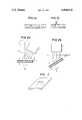
- FIG. 1(a)is an enlarged cross-sectional view of a light-sensitive glass plate in which holes have been formed by the conventional method
- FIG. 1(b)is an enlarged cross-sectional view of a light-sensitive glass plate in which holes have been formed by the exposure method of the present invention
- FIGS. 2(a) and 2(b)are schematic illustrative views of the method of the present invention.
- FIG. 3is a perspective view of a light-sensitive glass plate in which the desired hole is formed by application of a hydrofluoric acid solution after the irradiation with a parallel bundle of ultraviolet rays according to the method of the present invention.
- FIGS. 2(a) and 2(b)illustrate the positional relationship between a light source 1 capable of generating a parallel bundle of ultraviolet rays, a chemically machinable light-sensitive glass plate 2, and a mask 3 having openings of a desired form.
- the mask 3is mounted on the surface of the light-sensitive glass plate 2.
- the light source 1 and the light-sensitive glass plate 2face each other through the mask 3, and they are positioned so that an acute angle ⁇ formed between a plane A which is perpendicular to the parallel bundle of ultraviolet rays and a plane which is parallel to the surface of the glass plate 2 is equal to the desired taper angle (see FIG. 1(b)).
- the light-sensitive glass plate 2is exposed to the parallel bundle of ultraviolet rays from the light source 1 while the light-sensitive glass plate is rotated about a vertical central line B.
- the light source 1can revolve about the vertical central line B.
- the light-sensitive glass plate 2is exposed to the parallel bundle of ultraviolet rays from the light source 1 while rotating the light-sensitive glass plate 2 about a central line C of the parallel bundle of ultraviolet rays as an axis of rotation.
- the revolving motion of the light sourceis difficult to perform and requires that a relatively large amount of motion be induced as compared with the motion generated by rotating the light-sensitive glass plate. Therefore, for practical purposes, it is recommended that the light-sensitive glass plate 2 be rotated with the central line B or C forming the axis of rotation.
- the speed of rotation of the light-sensitive glass plate or light sourceis controlled depending on the output of the light source and the thickness of the light-sensitive glass plate. For example, when a 600 W Xe-Hg lamp is used as a light source, the light-sensitive glass plate is exposed to the parallel bundle of ultraviolet rays while rotating the light-sensitive glass plate or light source at a speed of rotation of once per minute and the glass plate is then heat treated at 590° C. for one hour. Thereafter, by etching the thus treated light-sensitive glass plate in a 5% hydrofluoric acid solution for three hours, a tapered hole as shown in FIG. 3 can be formed in a 1 mm thick light-sensitive glass plate.
- the etching treatmentis applied from only one side of the glass plate since when the etching treatment is applied from both sides of the glass plate, the hole swells near a central part of the hole and, therefore, it is not possible to form a hole tapered at a predetermined angle.
- holes or slits tapered at a desired anglecan be formed in a light-sensitive glass plate by controlling the acute angle ⁇ as shown in FIGS. 2(a) and 2(b).
- the method of the inventionis very useful in the preparation of cell sheets for plasma display and the like.
Landscapes
- Chemical & Material Sciences (AREA)
- Geochemistry & Mineralogy (AREA)
- Life Sciences & Earth Sciences (AREA)
- Engineering & Computer Science (AREA)
- Chemical Kinetics & Catalysis (AREA)
- General Chemical & Material Sciences (AREA)
- Materials Engineering (AREA)
- Organic Chemistry (AREA)
- Health & Medical Sciences (AREA)
- Toxicology (AREA)
- General Physics & Mathematics (AREA)
- Physics & Mathematics (AREA)
- Surface Treatment Of Glass (AREA)
- Re-Forming, After-Treatment, Cutting And Transporting Of Glass Products (AREA)
Abstract
Description
1. Field of the Invention
The present invention is a method for irradiating a chemically machinable light-sensitive glass with a parallel bundle of ultraviolet rays to form tapered holes or slits in the light-sensitive glass.
2. Description of the Prior Art
Holes or slits are often formed in a chemically machinable light-sensitive glass by irradiating the glass with ultraviolet rays through a mask placed on the surface of the glass. After the irradiation, the glass is heated causing fine lithium metasilicate (SiO2 -Li2 O) crystals to grow in the irradiated area. When the thus irradiated and heated glass is treated with a hydrofluoric acid solution, the crystal area dissolves at a faster rate than the non-irradiated area of the glass forming holes or slits in the irradiated areas. The above method is used to make perforations, engravings, channels and cuttings in chemically machinable light-sensitive glass.
In accordance with the conventional method for irradiation with ultraviolet rays which has heretofore been used to perforate chemically machinable light-sensitive glass, a parallel bundle of ultraviolet rays is applied vertically or obliquely to the glass plate with a mask mounted thereon. The mask has openings corresponding in shape and dimension to holes to be formed in the glass plate. In the conventional method, the light source and the light-sensitive glass plate are always kept in the same relative positional relationship. Thus, the diameter of the holes finally formed in the glass plate by application of hydrofluoric acid solution treatment is uniform in the direction of thickness of the glass even though the holes may be oriented vertically or obliquely relative to the glass plate. Typical holes formed by the conventional method are shown in FIG. 1(a). As can be seen, it is not possible to produce tapered holes such as those shown in FIG. 1(b) wherein the hole diameter increases in the direction of thickness of the glass plate according to the conventional method.
Accordingly, an object of the present invention is to provide a method for irradiation of chemically machinable light-sensitive glass with a parallel bundle of ultraviolet rays which permits the formation of tapered holes or slits as shown in FIG. 1(b) in the glass when the irradiated glass is heated and then treated with a hydrofluoric acid solution.
In the present invention, a mask having an opening therein is mounted on a surface of a glass plate and the plate is disposed below a light source which is capable of generating a parallel bundle of ultraviolet rays in such a manner that the ultraviolet rays enter the glass at a predetermined angle of incidence. The mask and glass plate are then rotated about a center axis of the glass plate. Alternatively, the light source can be revolved about a center axis of the glass plate. The glass plate is then heated and etched with acid in the conventional manner.
FIG. 1(a) is an enlarged cross-sectional view of a light-sensitive glass plate in which holes have been formed by the conventional method;
FIG. 1(b) is an enlarged cross-sectional view of a light-sensitive glass plate in which holes have been formed by the exposure method of the present invention;
FIGS. 2(a) and 2(b) are schematic illustrative views of the method of the present invention; and
FIG. 3 is a perspective view of a light-sensitive glass plate in which the desired hole is formed by application of a hydrofluoric acid solution after the irradiation with a parallel bundle of ultraviolet rays according to the method of the present invention.
FIGS. 2(a) and 2(b) illustrate the positional relationship between a light source 1 capable of generating a parallel bundle of ultraviolet rays, a chemically machinable light-sensitive glass plate 2, and amask 3 having openings of a desired form. Themask 3 is mounted on the surface of the light-sensitive glass plate 2. The light source 1 and the light-sensitive glass plate 2 face each other through themask 3, and they are positioned so that an acute angle α formed between a plane A which is perpendicular to the parallel bundle of ultraviolet rays and a plane which is parallel to the surface of theglass plate 2 is equal to the desired taper angle (see FIG. 1(b)).
In accordance with an embodiment of the method of the invention, as illustrated in FIG. 2(a), the light-sensitive glass plate 2 is exposed to the parallel bundle of ultraviolet rays from the light source 1 while the light-sensitive glass plate is rotated about a vertical central line B. Alternatively, the light source 1 can revolve about the vertical central line B.
In the other embodiment of the method of the invention, as illustrated in FIG. 2(b), the light-sensitive glass plate 2 is exposed to the parallel bundle of ultraviolet rays from the light source 1 while rotating the light-sensitive glass plate 2 about a central line C of the parallel bundle of ultraviolet rays as an axis of rotation.
In general, the revolving motion of the light source is difficult to perform and requires that a relatively large amount of motion be induced as compared with the motion generated by rotating the light-sensitive glass plate. Therefore, for practical purposes, it is recommended that the light-sensitive glass plate 2 be rotated with the central line B or C forming the axis of rotation.
The speed of rotation of the light-sensitive glass plate or light source is controlled depending on the output of the light source and the thickness of the light-sensitive glass plate. For example, when a 600 W Xe-Hg lamp is used as a light source, the light-sensitive glass plate is exposed to the parallel bundle of ultraviolet rays while rotating the light-sensitive glass plate or light source at a speed of rotation of once per minute and the glass plate is then heat treated at 590° C. for one hour. Thereafter, by etching the thus treated light-sensitive glass plate in a 5% hydrofluoric acid solution for three hours, a tapered hole as shown in FIG. 3 can be formed in a 1 mm thick light-sensitive glass plate.
It is preferred to apply the etching treatment from only one side of the glass plate since when the etching treatment is applied from both sides of the glass plate, the hole swells near a central part of the hole and, therefore, it is not possible to form a hole tapered at a predetermined angle.
In accordance with the method of the invention, holes or slits tapered at a desired angle can be formed in a light-sensitive glass plate by controlling the acute angle α as shown in FIGS. 2(a) and 2(b). Thus, the method of the invention is very useful in the preparation of cell sheets for plasma display and the like.
Claims (8)
1. A method for irradiating a chemically machinable light-sensitive glass plate with a parallel bundle of ultraviolet rays, comprising the steps of:
mounting a mask having an opening therein on a surface of said glass plate;
mounting a light source capable of generating said parallel bundle of ultraviolet rays above said mask so that an angle formed between a plane which is perpendicular to said parallel bundle of ultraviolet rays and a plane which is parallel to said surface of said glass plate is equal to a desired taper angle;
irradiating said plate with said parallel bundle of ultraviolet rays; and
rotating said glass plate about a center axis thereof.
2. The method claimed in claim 1 wherein said center axis is perpendicular to said surface of said glass plate.
3. The method claimed in claim 1 wherein said center axis is parallel to said parallel bundle of ultraviolet rays.
4. The method claimed in claim 2 or 3 further comprising the step of heating said glass plate to form lithium metasilicate crystals.
5. The method claimed in claim 4 further comprising the step of treating said glass plate with a hydrofluoric acid solution on only one side of said glass plate.
6. A method for irradiating a chemically machinable light-sensitive glass plate with a parallel bundle of ultraviolet rays, comprising the steps of:
mounting a mask having an opening therein on a surface of said glass plate;
mounting a light source capable of generating said parallel bundle of ultraviolet rays over said mask so that an angle formed between a plane which is perpendicular to said parallel bundle of ultraviolet rays and a plane which is parallel to said surface of said glass plate is equal to a desired taper angle;
irradiating said plate with said parallel bundle of ultraviolet rays; and
revolving said light source about a center axis of said glass plate, said center axis being perpendicular to said surface of said glass plate.
7. The method claimed in claim 6 further comprising the step of heating said glass plate to form lithium metasilicate crystals.
8. The method claimed in claim 7 further comprising the step of treating said glass plate with a hydrofluoric acid solution on only one side of said glass plate.
Applications Claiming Priority (2)
| Application Number | Priority Date | Filing Date | Title |
|---|---|---|---|
| JP56-83843 | 1981-06-02 | ||
| JP56083843AJPS57200042A (en) | 1981-06-02 | 1981-06-02 | Exposure method for chemically machinable photosensitive glass |
Publications (1)
| Publication Number | Publication Date |
|---|---|
| US4444616Atrue US4444616A (en) | 1984-04-24 |
Family
ID=13813983
Family Applications (1)
| Application Number | Title | Priority Date | Filing Date |
|---|---|---|---|
| US06/384,111Expired - Fee RelatedUS4444616A (en) | 1981-06-02 | 1982-06-01 | Method for exposure of chemically machinable light-sensitive glass |
Country Status (2)
| Country | Link |
|---|---|
| US (1) | US4444616A (en) |
| JP (1) | JPS57200042A (en) |
Cited By (31)
| Publication number | Priority date | Publication date | Assignee | Title |
|---|---|---|---|---|
| EP0179925A4 (en)* | 1984-05-01 | 1986-09-23 | Masataka Negishi | Method of forming non-continuous films on rugged or wavy surface of object. |
| US4662985A (en)* | 1985-03-27 | 1987-05-05 | Fuji Photo Film Co., Ltd. | Method of smoothing out an irregular surface of an electronic device |
| US4771012A (en)* | 1986-06-13 | 1988-09-13 | Matsushita Electric Industrial Co., Ltd. | Method of making symmetrically controlled implanted regions using rotational angle of the substrate |
| US4906594A (en)* | 1987-06-12 | 1990-03-06 | Agency Of Industrial Science And Technology | Surface smoothing method and method of forming SOI substrate using the surface smoothing method |
| US4918027A (en)* | 1985-03-05 | 1990-04-17 | Matsushita Electric Industrial Co., Ltd. | Method of fabricating semiconductor device |
| EP0373329A3 (en)* | 1988-12-16 | 1991-10-09 | Forschungszentrum Karlsruhe GmbH | Process for the lithographic production of galvanically shaped microstructures having a triangular or trapezoidal cross-section |
| US5086297A (en)* | 1988-06-14 | 1992-02-04 | Dai Nippon Insatsu Kabushiki Kaisha | Plasma display panel and method of forming fluorescent screen thereof |
| USRE35036E (en)* | 1986-06-13 | 1995-09-12 | Matsushita Electric Industrial Co., Ltd. | Method of making symmetrically controlled implanted regions using rotational angle of the substrate |
| US6127279A (en)* | 1994-09-26 | 2000-10-03 | Semiconductor Energy Laboratory Co., Ltd. | Solution applying method |
| EP1416325A1 (en)* | 2002-10-29 | 2004-05-06 | Corning Incorporated | A master and method of manufacturing a master for molds used to produce microstructured devices |
| FR2858694A1 (en)* | 2003-08-07 | 2005-02-11 | Commissariat Energie Atomique | Photolithographic process for microelectromechanical system fabrication, involves developing photosensitive resin layer to obtain patterns with inclined flanks relative to normal to substrates principal plane based on deviation angle |
| WO2005098486A1 (en)* | 2004-04-09 | 2005-10-20 | Kuraray Co., Ltd. | Method for manufacturing micro structure, method for manufacturing stamper using the micro structure and method for manufacturing resin micro structure using the stamper |
| US7132054B1 (en)* | 2004-09-08 | 2006-11-07 | Sandia Corporation | Method to fabricate hollow microneedle arrays |
| CN100483161C (en)* | 2007-04-13 | 2009-04-29 | 中国科学院上海微系统与信息技术研究所 | Slit arrangement and its preparing process |
| US20090162798A1 (en)* | 2006-08-18 | 2009-06-25 | Toppan Printing Co., Ltd. | Method of manufacturing master plate, method of manufacturing microneedle patch and apparatus exposure apparatus |
| WO2010080115A2 (en) | 2008-12-18 | 2010-07-15 | Claros Diagnostics, Inc. | Improved reagent storage in microfluidic systems and related articles and methods |
| WO2010087999A1 (en) | 2009-02-02 | 2010-08-05 | Claros Diagnostics, Inc. | Structures for controlling light interaction with microfluidic devices |
| US11101532B2 (en) | 2017-04-28 | 2021-08-24 | 3D Glass Solutions, Inc. | RF circulator |
| US11139582B2 (en) | 2018-09-17 | 2021-10-05 | 3D Glass Solutions, Inc. | High efficiency compact slotted antenna with a ground plane |
| US11161773B2 (en)* | 2016-04-08 | 2021-11-02 | 3D Glass Solutions, Inc. | Methods of fabricating photosensitive substrates suitable for optical coupler |
| US11264167B2 (en) | 2016-02-25 | 2022-03-01 | 3D Glass Solutions, Inc. | 3D capacitor and capacitor array fabricating photoactive substrates |
| US11270843B2 (en) | 2018-12-28 | 2022-03-08 | 3D Glass Solutions, Inc. | Annular capacitor RF, microwave and MM wave systems |
| US11342896B2 (en) | 2017-07-07 | 2022-05-24 | 3D Glass Solutions, Inc. | 2D and 3D RF lumped element devices for RF system in a package photoactive glass substrates |
| US11367939B2 (en) | 2017-12-15 | 2022-06-21 | 3D Glass Solutions, Inc. | Coupled transmission line resonate RF filter |
| US11373908B2 (en) | 2019-04-18 | 2022-06-28 | 3D Glass Solutions, Inc. | High efficiency die dicing and release |
| US11594457B2 (en) | 2018-12-28 | 2023-02-28 | 3D Glass Solutions, Inc. | Heterogenous integration for RF, microwave and MM wave systems in photoactive glass substrates |
| US11677373B2 (en) | 2018-01-04 | 2023-06-13 | 3D Glass Solutions, Inc. | Impedence matching conductive structure for high efficiency RF circuits |
| US11908617B2 (en) | 2020-04-17 | 2024-02-20 | 3D Glass Solutions, Inc. | Broadband induction |
| US11929199B2 (en) | 2014-05-05 | 2024-03-12 | 3D Glass Solutions, Inc. | 2D and 3D inductors fabricating photoactive substrates |
| US11962057B2 (en) | 2019-04-05 | 2024-04-16 | 3D Glass Solutions, Inc. | Glass based empty substrate integrated waveguide devices |
| US12165809B2 (en) | 2016-02-25 | 2024-12-10 | 3D Glass Solutions, Inc. | 3D capacitor and capacitor array fabricating photoactive substrates |
Families Citing this family (5)
| Publication number | Priority date | Publication date | Assignee | Title |
|---|---|---|---|---|
| JPH0459628A (en)* | 1990-06-29 | 1992-02-26 | Seikosha Co Ltd | Processing of plate glass |
| JP4758200B2 (en)* | 2005-10-28 | 2011-08-24 | 京セラキンセキ株式会社 | Exposure apparatus and exposure method |
| JP4911682B2 (en)* | 2006-07-20 | 2012-04-04 | 富士フイルム株式会社 | Exposure equipment |
| JP4984736B2 (en)* | 2006-08-18 | 2012-07-25 | 凸版印刷株式会社 | Exposure apparatus and method |
| JP5070764B2 (en)* | 2006-08-18 | 2012-11-14 | 凸版印刷株式会社 | Microneedle patch manufacturing method |
Citations (2)
| Publication number | Priority date | Publication date | Assignee | Title |
|---|---|---|---|---|
| US2628160A (en)* | 1951-08-30 | 1953-02-10 | Corning Glass Works | Sculpturing glass |
| US4276335A (en)* | 1978-03-13 | 1981-06-30 | General Electric Company | Electron beam matrix deflector and method of fabrication |
Family Cites Families (1)
| Publication number | Priority date | Publication date | Assignee | Title |
|---|---|---|---|---|
| JPS49133782A (en)* | 1973-04-28 | 1974-12-23 |
- 1981
- 1981-06-02JPJP56083843Apatent/JPS57200042A/enactiveGranted
- 1982
- 1982-06-01USUS06/384,111patent/US4444616A/ennot_activeExpired - Fee Related
Patent Citations (2)
| Publication number | Priority date | Publication date | Assignee | Title |
|---|---|---|---|---|
| US2628160A (en)* | 1951-08-30 | 1953-02-10 | Corning Glass Works | Sculpturing glass |
| US4276335A (en)* | 1978-03-13 | 1981-06-30 | General Electric Company | Electron beam matrix deflector and method of fabrication |
Cited By (39)
| Publication number | Priority date | Publication date | Assignee | Title |
|---|---|---|---|---|
| EP0179925A4 (en)* | 1984-05-01 | 1986-09-23 | Masataka Negishi | Method of forming non-continuous films on rugged or wavy surface of object. |
| US4918027A (en)* | 1985-03-05 | 1990-04-17 | Matsushita Electric Industrial Co., Ltd. | Method of fabricating semiconductor device |
| US4662985A (en)* | 1985-03-27 | 1987-05-05 | Fuji Photo Film Co., Ltd. | Method of smoothing out an irregular surface of an electronic device |
| US4771012A (en)* | 1986-06-13 | 1988-09-13 | Matsushita Electric Industrial Co., Ltd. | Method of making symmetrically controlled implanted regions using rotational angle of the substrate |
| USRE35036E (en)* | 1986-06-13 | 1995-09-12 | Matsushita Electric Industrial Co., Ltd. | Method of making symmetrically controlled implanted regions using rotational angle of the substrate |
| US4906594A (en)* | 1987-06-12 | 1990-03-06 | Agency Of Industrial Science And Technology | Surface smoothing method and method of forming SOI substrate using the surface smoothing method |
| US5086297A (en)* | 1988-06-14 | 1992-02-04 | Dai Nippon Insatsu Kabushiki Kaisha | Plasma display panel and method of forming fluorescent screen thereof |
| EP0373329A3 (en)* | 1988-12-16 | 1991-10-09 | Forschungszentrum Karlsruhe GmbH | Process for the lithographic production of galvanically shaped microstructures having a triangular or trapezoidal cross-section |
| US6127279A (en)* | 1994-09-26 | 2000-10-03 | Semiconductor Energy Laboratory Co., Ltd. | Solution applying method |
| US20050064641A1 (en)* | 1994-09-26 | 2005-03-24 | Semiconductor Energy Laboratory Co., Ltd. | Solution applying apparatus and method |
| US7271109B2 (en) | 1994-09-26 | 2007-09-18 | Semiconductor Energy Laboratory Co., Ltd. | Solution applying apparatus and method |
| EP1416325A1 (en)* | 2002-10-29 | 2004-05-06 | Corning Incorporated | A master and method of manufacturing a master for molds used to produce microstructured devices |
| FR2858694A1 (en)* | 2003-08-07 | 2005-02-11 | Commissariat Energie Atomique | Photolithographic process for microelectromechanical system fabrication, involves developing photosensitive resin layer to obtain patterns with inclined flanks relative to normal to substrates principal plane based on deviation angle |
| WO2005017623A3 (en)* | 2003-08-07 | 2005-10-06 | Commissariat Energie Atomique | $m(c)method for producing inclined flank patterns by photolithography |
| US20070003839A1 (en)* | 2003-08-07 | 2007-01-04 | Marc Rabarot | $M(c)method for producing inclined flank patterns by photolithography |
| WO2005098486A1 (en)* | 2004-04-09 | 2005-10-20 | Kuraray Co., Ltd. | Method for manufacturing micro structure, method for manufacturing stamper using the micro structure and method for manufacturing resin micro structure using the stamper |
| US7132054B1 (en)* | 2004-09-08 | 2006-11-07 | Sandia Corporation | Method to fabricate hollow microneedle arrays |
| US20090162798A1 (en)* | 2006-08-18 | 2009-06-25 | Toppan Printing Co., Ltd. | Method of manufacturing master plate, method of manufacturing microneedle patch and apparatus exposure apparatus |
| US8062835B2 (en) | 2006-08-18 | 2011-11-22 | Toppan Printing Co., Ltd. | Method of manufacturing master plate, method of manufacturing microneedle patch and apparatus exposure apparatus |
| CN100483161C (en)* | 2007-04-13 | 2009-04-29 | 中国科学院上海微系统与信息技术研究所 | Slit arrangement and its preparing process |
| WO2010080115A2 (en) | 2008-12-18 | 2010-07-15 | Claros Diagnostics, Inc. | Improved reagent storage in microfluidic systems and related articles and methods |
| WO2010087999A1 (en) | 2009-02-02 | 2010-08-05 | Claros Diagnostics, Inc. | Structures for controlling light interaction with microfluidic devices |
| EP3278877A1 (en) | 2009-02-02 | 2018-02-07 | Opko Diagnostics, LLC | Structures for controlling light interaction with microfluidic devices |
| DE202010018623U1 (en) | 2009-02-02 | 2018-12-07 | Opko Diagnostics, Llc | Structures for controlling the light interaction with microfluidic devices |
| US11929199B2 (en) | 2014-05-05 | 2024-03-12 | 3D Glass Solutions, Inc. | 2D and 3D inductors fabricating photoactive substrates |
| US11264167B2 (en) | 2016-02-25 | 2022-03-01 | 3D Glass Solutions, Inc. | 3D capacitor and capacitor array fabricating photoactive substrates |
| US12165809B2 (en) | 2016-02-25 | 2024-12-10 | 3D Glass Solutions, Inc. | 3D capacitor and capacitor array fabricating photoactive substrates |
| US11161773B2 (en)* | 2016-04-08 | 2021-11-02 | 3D Glass Solutions, Inc. | Methods of fabricating photosensitive substrates suitable for optical coupler |
| US11101532B2 (en) | 2017-04-28 | 2021-08-24 | 3D Glass Solutions, Inc. | RF circulator |
| US11342896B2 (en) | 2017-07-07 | 2022-05-24 | 3D Glass Solutions, Inc. | 2D and 3D RF lumped element devices for RF system in a package photoactive glass substrates |
| US11367939B2 (en) | 2017-12-15 | 2022-06-21 | 3D Glass Solutions, Inc. | Coupled transmission line resonate RF filter |
| US11894594B2 (en) | 2017-12-15 | 2024-02-06 | 3D Glass Solutions, Inc. | Coupled transmission line resonate RF filter |
| US11677373B2 (en) | 2018-01-04 | 2023-06-13 | 3D Glass Solutions, Inc. | Impedence matching conductive structure for high efficiency RF circuits |
| US11139582B2 (en) | 2018-09-17 | 2021-10-05 | 3D Glass Solutions, Inc. | High efficiency compact slotted antenna with a ground plane |
| US11594457B2 (en) | 2018-12-28 | 2023-02-28 | 3D Glass Solutions, Inc. | Heterogenous integration for RF, microwave and MM wave systems in photoactive glass substrates |
| US11270843B2 (en) | 2018-12-28 | 2022-03-08 | 3D Glass Solutions, Inc. | Annular capacitor RF, microwave and MM wave systems |
| US11962057B2 (en) | 2019-04-05 | 2024-04-16 | 3D Glass Solutions, Inc. | Glass based empty substrate integrated waveguide devices |
| US11373908B2 (en) | 2019-04-18 | 2022-06-28 | 3D Glass Solutions, Inc. | High efficiency die dicing and release |
| US11908617B2 (en) | 2020-04-17 | 2024-02-20 | 3D Glass Solutions, Inc. | Broadband induction |
Also Published As
| Publication number | Publication date |
|---|---|
| JPS57200042A (en) | 1982-12-08 |
| JPH0136095B2 (en) | 1989-07-28 |
Similar Documents
| Publication | Publication Date | Title |
|---|---|---|
| US4444616A (en) | Method for exposure of chemically machinable light-sensitive glass | |
| US4390391A (en) | Method of exposure of chemically machineable light-sensitive glass | |
| DE69707118T2 (en) | METHOD FOR PRODUCING A GLASS ARTICLE | |
| JPS606503B2 (en) | How to manufacture parts | |
| EP0273547A3 (en) | A method for producing amorphous metal layer | |
| ATE142048T1 (en) | PROCESS FOR PRODUCING A CRYSTAL AND CRYSTAL PRODUCED THEREFORE | |
| US6008467A (en) | Laser processing method to an optical waveguide | |
| JPH05139785A (en) | Working method for photosensitive glass | |
| US4404060A (en) | Method for producing insulating ring zones by galvanic and etch technologies at orifice areas of through-holes in a plate | |
| JPS59182529A (en) | Method of patterning semiconductor layer | |
| JPH03232731A (en) | Method for dividing chemical cuttable photosensitive glass product | |
| JP3797703B2 (en) | Laser processing method for glass substrate | |
| JPS55127016A (en) | Manufacturing of semiconductor device | |
| JPS55143035A (en) | Manufacture of pattern | |
| JP2529141B2 (en) | Liquid crystal substrate manufacturing method | |
| JPS58152241A (en) | Manufacture of high-precision mask | |
| DE3118335A1 (en) | Method of structuring (patterning) plates with insulating annular zones in the vicinity of the openings of holes by electroplating and etching | |
| JPS60102740A (en) | Semiconductor device manufacturing equipment | |
| JP2612606B2 (en) | Method for producing photosensitive glass patterned article | |
| JP2521893B2 (en) | Wire guide manufacturing method | |
| JPS5792830A (en) | Manufacture of mask for x-ray exposure | |
| JPH0138061B2 (en) | ||
| JPS57173943A (en) | Manufacture of photo mask | |
| JPS56100417A (en) | Forming method for resist pattern | |
| JPH06227843A (en) | Method for forming stepped hole or groove in photosensitive glass plate |
Legal Events
| Date | Code | Title | Description |
|---|---|---|---|
| AS | Assignment | Owner name:HOYA CORPORATION, NO. 7-5, NAKAOCHIAI 2-CHOME, SHI Free format text:ASSIGNMENT OF ASSIGNORS INTEREST.;ASSIGNORS:FUJITA, YOSHIMI;YAMASHITA, TOSHIHARU;REEL/FRAME:004220/0718 Effective date:19820417 | |
| FEPP | Fee payment procedure | Free format text:PAYOR NUMBER ASSIGNED (ORIGINAL EVENT CODE: ASPN); ENTITY STATUS OF PATENT OWNER: LARGE ENTITY | |
| FPAY | Fee payment | Year of fee payment:4 | |
| FPAY | Fee payment | Year of fee payment:8 | |
| REMI | Maintenance fee reminder mailed | ||
| LAPS | Lapse for failure to pay maintenance fees | ||
| FP | Lapsed due to failure to pay maintenance fee | Effective date:19960424 | |
| STCH | Information on status: patent discontinuation | Free format text:PATENT EXPIRED DUE TO NONPAYMENT OF MAINTENANCE FEES UNDER 37 CFR 1.362 |