US4441155A - Page controlled cache directory addressing - Google Patents
Page controlled cache directory addressingDownload PDFInfo
- Publication number
- US4441155A US4441155AUS06/324,165US32416581AUS4441155AUS 4441155 AUS4441155 AUS 4441155AUS 32416581 AUS32416581 AUS 32416581AUS 4441155 AUS4441155 AUS 4441155A
- Authority
- US
- United States
- Prior art keywords
- cache
- page
- bit position
- field
- address
- Prior art date
- Legal status (The legal status is an assumption and is not a legal conclusion. Google has not performed a legal analysis and makes no representation as to the accuracy of the status listed.)
- Expired - Lifetime
Links
Images


Classifications
- G—PHYSICS
- G06—COMPUTING OR CALCULATING; COUNTING
- G06F—ELECTRIC DIGITAL DATA PROCESSING
- G06F12/00—Accessing, addressing or allocating within memory systems or architectures
- G06F12/02—Addressing or allocation; Relocation
- G06F12/08—Addressing or allocation; Relocation in hierarchically structured memory systems, e.g. virtual memory systems
- G06F12/0802—Addressing of a memory level in which the access to the desired data or data block requires associative addressing means, e.g. caches
- G06F12/0864—Addressing of a memory level in which the access to the desired data or data block requires associative addressing means, e.g. caches using pseudo-associative means, e.g. set-associative or hashing
Definitions
- the inventionrelates to an improvement in the addressing controls for a processor cache in a data processing system.
- the most commonly used cache directory found in current commercial computer systemsis a hardware matrix in which the matrix rows contain respective cache congruence classes, in which each class has a plurality of associative entries, and each entry is capable of containing a main storage address representation for a line of words in an associated cache data storage array.
- the directory entriesmay be conceptually considered to be arranged in the respective columns (i.e. sets) of the matrix. The entries in any row found in the different columns are set-associative.
- Each CPU storage requested address(whether virtual or real) is directed to the cache directory.
- the requested addresscan be logically divided into a plurality of fields, such as: an external page address field and an internal page address field.
- the external address fieldis the high-order part of the requested address and addresses a page frame in main storage, and it requires translation for a virtual address.
- the remaining low-order part of the requested addressis the internal page address field and addresses a byte location within the addressed page.
- the internal page address fieldis subdivided into a congruence class address (CCA) field, a word address field, and a byte address field.
- CCAcongruence class address
- the CCA fieldaddresses the cache directory to select a required congruence class.
- a line addressis resolved for the cache.
- the word address fieldlocates a word in that cache line, and the byte address field finds the required byte location in the addressed word.
- the congruence class address (CCA) fieldis formed from an internal part of the CPU requested address and comprises K number of consecutive bits providing a line address field within the internal page address field.
- Congruence class addresses provided for the rows in the cache directoryare generally numbered in zero-origin fashion, with a value between 0 and TCC-1, inclusive, in which TCC is the total number of congruence classes in the cache directory.
- Log TCCbase 2 determines the K number of bits in each CCA. For example, assume a cache directory has 32 congruence classes, four entries in each class, and that each entry can represent the address for a line of 16 doublewords in an associated cache. Each doubleword contains 8 bytes. Thus, the associated cache can contain 16,384 bytes (i.e.
- each CCAwill have five bits (i.e. log 2 32). Therefore, the CCA is a five bit field selected from each requested address, for example, bit positions 20 through 24 in a 32 bit address word.
- Bit 19 in the request addressis the lowest-order bit in the external page address for a 4096 byte page size. Therefore, in any 24 bit address found in a 32 bit position word in the IBM System/370 computers, bit positions 8-19 provide the external page address field, and bit positions 20 through 31 in a requested address provide the internal page address field.
- the cache addressingcontrols map the requested data line addresses into entries in the cache directory congruence classes in accordance with the CPU requested address.
- the inventors of this applicationhave found that the most frequently selected cache congruence classes are at class addresses which map near the low and high boundaries of a page, and the frequency of cache class selection generally decreases as the requested addresses deviate away from the lowest and highest addresses toward the intermediate addresses within a page.
- This cache class frequency of use characteristicis reflected in the miss rate observed for different congruence classes.
- the more uniform frequency of class usereduces the cache miss rate to correspondingly improve the processor performance.
- This inventionsenses at least the lowest-order bit in the external page address field in the CPU requested address and uses the value of this bit to control the inversion of the second highest-order bit position in a congruence class selection field which is obtained from the high-order part of the internal page address field in the CPU requested address for generating a congruence class address (CCA) that modifies the frequency distribution of class use in a cache directory in accordance with this invention.
- CCAcongruence class address
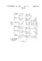
- FIGS. 1 and 2illustrate the fields in a CPU requested address and their relationship to the subject invention.
- FIG. 3shows how the invention is located in an otherwise conventional cache directory arrangement.
- FIGS. 4 and 5illustrate alternative implementations of the invention.
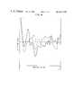
- FIG. 6illustrates the request misses in the congruence classes of a cache without and with the invention.
- FIG. 1represents the fields and their bit positions in a CPU request address for an example of a cache directory with 32 congruence classes which therefore require a five bit position CCA.
- a group comprised of the six bit positions 19 through 24(which includes the congruence class selection field comprised of bit positions 20-24) is obtained from a CPU request address in a word comprised of bit positions 0-31, in order to generate the five bit position CCA.
- the six bit group (19-24)is then manipulated by this invention as follows to generate the five bit CCA:
- bit position 19is 1, bit position 21 is inverted.
- bit position 19is 0, bit position 21 is unchanged.
- bit position 19is then discarded and the resulting five bit positions 20-24 are used as the CCA.
- FIG. 2similarly represents the fields and bit positions in a CPU requested address for another example of a cache directory with 128 congruence classes, and therefore requiring a seven bit CCA comprised of bit positions 18-24 of the CPU requested address.
- bit positions 18, 19are used from a CPU requested virtual address, ambiguity in synonym class addressing can result in a cache directory which can be resolved in the manner disclosed and claimed in U.S. patent application Ser. No. 130,946 filed Mar. 17, 1980 by B. U. Messina et al, entitled "Cache Synonym Detection And Handling Mechanism" and assigned to the same assignee as the subject application.
- 130,946uses the synonym effect of bits 18, 19 to divide the cache directory into four synonym groups according to the four permuted values for bit positions 18, 19 in which each synonym group has 32 congruence classes.
- the congruence classis selected in the same manner as previously described, as follows:
- a or Bonly use bit positions 20-24 to select the required congruence class in the resolved synonym group (e.g. resolved by a principle/synonym hit determination).
- the operation of this inventiondepends on the following rules:
- the 0 and 1 values of the highest-order internal page address bit(e.g. bit position 20) divide a page location into upper and lower halves.
- the 0 and 1 values of the second highest-order internal page address bit(e.g. bit position 21) divides the respective half of a page (determined by the value of bit position 20) into upper and lower quarters of a page, respectively (i.e. complementary quarters).
- the 0 and 1 values of the third highest-order internal page address bit(e.g. bit position 22) divides the respective quarter of a page (determined by the values of bit positions 20, 21) into upper and lower one-eighths of a page. Each subsequently lower-order bit position will therefore divide a respectively smaller page portion into upper and lower halves.
- the resulting CCA(which depends on internal page address bit positions 20-24) can relocate in the cache directory to another CCA found in the complementary quarter of the page.
- the subject inventionSince the subject invention is based on a statistical discovery that the internal page address use pattern derived from computer job streams shows the highest use frequency of lines to be at the lower and upper addresses in the average page and the lowest use frequency in the intermediate addresses, the invention implements the quarter page inversion by inverting the second highest-order internal page addressing bit position (e.g. 21) as the most effective bit position for controlling the redistribution of storage references among the congruence classes in a more uniform manner to obtain a more even statistical frequency of use of all the different classes in the cache directory and thereby reduce the frequency of cache misses.
- the second highest-order internal page addressing bit positione.g. 21
- an effective way to control the quarter page redistributions by the second-highest order internal page address bit positionis to use the value of the lowest-order external page address bit position (e.g. 19), since it changes more often than any higher-order bit used to address a page in storage.
- the experimental conclusionwas therefore to use the value of the lowest-order external page address bit position (e.g. 19), to control the inverting of the second highest-order internal page address bit position (e.g. 21).
- external page address bit positionsmay also be used in addition to the lowest-order bit position (e.g. 19) to provide less significant class-redistribution refinements, for example, by exclusive-ORing them so that the internal page second-order bit is inverted whenever any of the selected external page bits changes to a one state.
- FIGS. 3-5shows only the preferred second highest-order page address bit position 21 being controlled by the lowest-order external page address bit position 19, in order to minimize hardware and timing problems which can result in different path length delays within the cache addressing circuits which are critical to obtaining fast cache performance.
- column CCAindicates all of the cache's congruence class addresses in hexadecimal numbers.
- the results with the inventionare represented in column ICCA, which shows the proportion % of cache misses in each congruence class when using the invention.
- the results with the conventional cacheare represented in column CCCA which shows the proportion % of cache misses for its respective congruence classes.
- % CHANGEindicates the net deviation gain (+) or loss (-) for the corresponding congruence classes.
- the net deviation for all 32 congruence classes in the cacheindicates that the invention obtains a 3.6% decrease in cache misses which results in a correspondingly significant improvement in CPU performance for a very small increase (i.e. much less than 3.6%) in hardware costs to incorporate the subject invention into a cache directory in a CPU being manufactured.
- Profile 71 in FIG. 6shows the typical distribution of cache misses as a function of the congruence class addresses (CCAs) in a conventional cache directory.
- Profile 72shows a typical distribution of the cache misses as a function of the CCAs in a cache directory having this invention.
- a visual comparison of profiles 71 and 72shows that the invention obtains a more uniform distribution (i.e. closer to average profile 73) than the conventional cache. The more uniform distribution results in a reduction in cache misses which improves processor performance.
- FIG. 3illustrates a cache directory hardware arrangement which contains the method provided by the subject invention in its class selection control circuits 10, that may be constructed as shown in either FIG. 4 or FIG. 5. Circuits 10 receive a requested logical address provided from a CPU (not shown).
- a congruence class addressis outputted from circuits 10 to conventional cache directory circuits, such as to a conventional type of address decoder 11 for a set-associative cache directory 12 which are shown for the purpose of illustrating how the cache addressing circuits 10 containing the invention connect to cache circuits which may be conventional. Accordingly, the output of circuit 10 selects one of 32 congruence classes having class addresses 0-31 in cache directory 12. Each congruence class contains four entries A, B, C, and D. All four entries in any selected congruence class are examined associatively, and this type of cache directory is commonly called set-associative.
- a conventional directory register 13receives the four set-associative entries in any selected congruence class in cache directory 12.
- Conventional directory compare logiccompares the four entries A, B, C, and D in register 13 with a translated absolute address corresponding to the CPU requested logical address. The results of this compare enables one of exclusive-OR circuits 16, 17, 18 or 19 in the conventional manner to select one of the set addresses A, B, C, or D and output it to the associated cache to select the proper line of data in the addressed class.
- the requested doubleword (DW) in the selected cache lineis addressed by the cache DW selection field derived from the CPU requested logical address. The CPU will use the byte selection field to obtain the required byte location in the DW.
- FIGS. 4 and 5respectively illustrate two embodiments of the subject invention. Each embodiment receives a part of the CPU requested logical address, i.e. address bits 19-24. Also, each embodiment in FIG. 4 or 5 provides a congruence class address (CCA) which is provided to address decoder 11 in FIG. 3.
- CCAcongruence class address
- the choice between the embodiments in FIG. 4 or 5depends on the time delay skew for the address bits in the cache congruence class address outputted from circuits 10 in FIG. 3 in a particular cache design.
- the path having the longest delay in the designis sometimes known as the "critical path".
- the embodiment in FIG. 4is preferable if an exclusive-OR circuit 31 provided for this invention is not in the critical path.
- exclusive-OR circuit 31should be in the critical path of a particular cache directory design, then the alternative circuitry provided by in FIG. 5 is preferable, since it places circuits provided by this invention in other path relationships by providing exclusive-OR circuits 41 and 42 on the output side of a congruence class address register.
- an exclusive-OR circuit 31receives logical address bit positions 19 and 21 and its output is connected to an AND gate 36.
- AND gates 35, 37, 38 and 39respectively receive logical address bits 20, 22, 23, and 24.
- Gates 35-39gate them to set inputs of triggers 41-45 (comprising a CCA register) when a set signal is received from the CPU on a line 33.
- the true (t) and complementary (c) outputs of triggers 41-45provide the CCA bits to the address decoder 11 in FIG. 3 to select a congruence class.
- Triggers 41-45are reset by a CPU signal on a line 34.
- the alternative embodiment in FIG. 5provides exclusive-OR circuits 41 and 42 on the output side of the CCA register comprising triggers 61-66 which receive set inputs representing bit positions 19-24 from AND gates 54-59.
- the CCA registerrespectively receives request address bits 19-24.
- the CPUprovides a reset signal to the reset line 33 for resetting the congruence class register 41-45 or 61-66 when the next CPU request is going to be provided.
- Exclusive-OR circuit 41generates the complement signal for CCA bit position 21 and exclusive-OR circuit 42 generates the true signal for CCA bit position 21 in the outputted CCA address provided to the address decoder 11.
Landscapes
- Engineering & Computer Science (AREA)
- Theoretical Computer Science (AREA)
- Physics & Mathematics (AREA)
- General Engineering & Computer Science (AREA)
- General Physics & Mathematics (AREA)
- Memory System Of A Hierarchy Structure (AREA)
Abstract
Description
TABLE 1 ______________________________________ CCCA ICCA % of % of % CCA MISSES MISSES CHANGE ______________________________________ 00 6.3 5.9 -0.4 01 5.0 4.3 -0.7 02 3.1 2.7 +0.4 03 2.4 1.8 +0.6 04 3.0 1.8 +1.2 05 3.4 2.7 +0.1 06 4.7 3.1 -1.6 07 4.3 3.2 -1.1 08 2.6 3.5 -0.1 09 3.0 3.6 -0.4 0A 2.3 2.8 -0.5 0B 1.6 2.3 -0.7 0C 1.2 2.1 -0.9 0D 2.2 2.9 -0.7 0E 2.6 3.4 -0.2 0F 2.5 3.4 -0.3 10 2.4 2.7 -0.3 11 2.7 3.5 0 12 2.7 3.4 -0.1 13 2.5 3.8 +0.1 14 3.0 3.6 +0.4 15 2.8 3.6 +0.2 16 3.3 3.6 +0.3 17 2.7 3.8 +0.3 18 3.9 3.6 -0.3 19 3.6 2.9 -0.3 1A 3.1 2.6 +0.5 1B 3.3 2.3 +0.6 1C 2.9 2.1 +0.8 1D 3.7 3.2 -0.5 1E 3.3 2.9 0 1F 4.1 2.9 -0.8 -3.6 ______________________________________
Claims (9)
Priority Applications (4)
| Application Number | Priority Date | Filing Date | Title |
|---|---|---|---|
| US06/324,165US4441155A (en) | 1981-11-23 | 1981-11-23 | Page controlled cache directory addressing |
| JP57143537AJPS5891573A (en) | 1981-11-23 | 1982-08-20 | Cash address specifying method |
| DE8282109612TDE3279113D1 (en) | 1981-11-23 | 1982-10-18 | Page controlled cache directory addressing |
| EP82109612AEP0080062B1 (en) | 1981-11-23 | 1982-10-18 | Page controlled cache directory addressing |
Applications Claiming Priority (1)
| Application Number | Priority Date | Filing Date | Title |
|---|---|---|---|
| US06/324,165US4441155A (en) | 1981-11-23 | 1981-11-23 | Page controlled cache directory addressing |
Publications (1)
| Publication Number | Publication Date |
|---|---|
| US4441155Atrue US4441155A (en) | 1984-04-03 |
Family
ID=23262380
Family Applications (1)
| Application Number | Title | Priority Date | Filing Date |
|---|---|---|---|
| US06/324,165Expired - LifetimeUS4441155A (en) | 1981-11-23 | 1981-11-23 | Page controlled cache directory addressing |
Country Status (4)
| Country | Link |
|---|---|
| US (1) | US4441155A (en) |
| EP (1) | EP0080062B1 (en) |
| JP (1) | JPS5891573A (en) |
| DE (1) | DE3279113D1 (en) |
Cited By (36)
| Publication number | Priority date | Publication date | Assignee | Title |
|---|---|---|---|---|
| US4612612A (en)* | 1983-08-30 | 1986-09-16 | Amdahl Corporation | Virtually addressed cache |
| US4631660A (en)* | 1983-08-30 | 1986-12-23 | Amdahl Corporation | Addressing system for an associative cache memory |
| US4972338A (en)* | 1985-06-13 | 1990-11-20 | Intel Corporation | Memory management for microprocessor system |
| US4989178A (en)* | 1985-10-11 | 1991-01-29 | Omron Tateisi Electronics Co. | Programmable controller having forcibly set or reset I/O states controlled by stored flags in a flag memory |
| US5077826A (en)* | 1989-08-09 | 1991-12-31 | International Business Machines Corporation | Cache performance in an information handling system employing page searching |
| WO1992007323A1 (en)* | 1990-10-12 | 1992-04-30 | Intel Corporation | Cache controller and associated method for remapping cache address bits |
| US5119290A (en)* | 1987-10-02 | 1992-06-02 | Sun Microsystems, Inc. | Alias address support |
| US5133061A (en)* | 1987-10-29 | 1992-07-21 | International Business Machines Corporation | Mechanism for improving the randomization of cache accesses utilizing abit-matrix multiplication permutation of cache addresses |
| US5148538A (en)* | 1989-10-20 | 1992-09-15 | International Business Machines Corporation | Translation look ahead based cache access |
| US5210843A (en)* | 1988-03-25 | 1993-05-11 | Northern Telecom Limited | Pseudo set-associative memory caching arrangement |
| US5371876A (en)* | 1991-05-10 | 1994-12-06 | Intel Corporation | Computer system with a paged non-volatile memory |
| US5493668A (en)* | 1990-12-14 | 1996-02-20 | International Business Machines Corporation | Multiple processor system having software for selecting shared cache entries of an associated castout class for transfer to a DASD with one I/O operation |
| US5579522A (en)* | 1991-05-06 | 1996-11-26 | Intel Corporation | Dynamic non-volatile memory update in a computer system |
| US5822581A (en)* | 1995-09-29 | 1998-10-13 | Intel Corporation | Method for CMOS configuration information storage and retrieval in flash |
| US5835928A (en)* | 1993-12-22 | 1998-11-10 | International Business Machines Corporation | Circuitry and method for relating first and second memory locations where the second memory location stores information from the first memory location |
| US5838893A (en)* | 1996-12-26 | 1998-11-17 | Microsoft Corporation | Method and system for remapping physical memory |
| US5930504A (en)* | 1996-07-22 | 1999-07-27 | Intel Corporation | Dynamic nonvolatile memory update in a computer system |
| US5978791A (en)* | 1995-04-11 | 1999-11-02 | Kinetech, Inc. | Data processing system using substantially unique identifiers to identify data items, whereby identical data items have the same identifiers |
| US6014709A (en)* | 1997-11-05 | 2000-01-11 | Unisys Corporation | Message flow protocol for avoiding deadlocks |
| US6049849A (en)* | 1997-04-14 | 2000-04-11 | International Business Machines Corporation | Imprecise method and system for selecting an alternative cache entry for replacement in response to a conflict between cache operation requests |
| US6049845A (en)* | 1997-11-05 | 2000-04-11 | Unisys Corporation | System and method for providing speculative arbitration for transferring data |
| US6052760A (en)* | 1997-11-05 | 2000-04-18 | Unisys Corporation | Computer system including plural caches and utilizing access history or patterns to determine data ownership for efficient handling of software locks |
| US6092156A (en)* | 1997-11-05 | 2000-07-18 | Unisys Corporation | System and method for avoiding deadlocks utilizing split lock operations to provide exclusive access to memory during non-atomic operations |
| US6145057A (en)* | 1997-04-14 | 2000-11-07 | International Business Machines Corporation | Precise method and system for selecting an alternative cache entry for replacement in response to a conflict between cache operation requests |
| US6212616B1 (en)* | 1998-03-23 | 2001-04-03 | International Business Machines Corporation | Even/odd cache directory mechanism |
| US6314501B1 (en) | 1998-07-23 | 2001-11-06 | Unisys Corporation | Computer system and method for operating multiple operating systems in different partitions of the computer system and for allowing the different partitions to communicate with one another through shared memory |
| US6421761B1 (en) | 1999-11-09 | 2002-07-16 | International Business Machines Corporation | Partitioned cache and management method for selectively caching data by type |
| US6430656B1 (en)* | 1999-09-07 | 2002-08-06 | International Business Machines Corporation | Cache and management method using combined software and hardware congruence class selectors |
| US6665761B1 (en) | 1999-07-28 | 2003-12-16 | Unisys Corporation | Method and apparatus for routing interrupts in a clustered multiprocessor system |
| US6687818B1 (en) | 1999-07-28 | 2004-02-03 | Unisys Corporation | Method and apparatus for initiating execution of an application processor in a clustered multiprocessor system |
| US6779102B2 (en)* | 1985-03-15 | 2004-08-17 | Hitachi, Ltd. | Data processor capable of executing an instruction that makes a cache memory ineffective |
| US20070220116A1 (en)* | 2006-03-14 | 2007-09-20 | Anthony Rose | Filter for a Distributed Network |
| US20070245087A1 (en)* | 2004-12-02 | 2007-10-18 | Fujitsu Limited | Data buffer device, cache device, and data buffer control method |
| US20080002511A1 (en)* | 2006-06-30 | 2008-01-03 | Chi Yuan Mou | Semiconductor memory and address-decoding circuit and method for decoding address |
| US7940706B2 (en) | 2001-10-01 | 2011-05-10 | International Business Machines Corporation | Controlling the state of duplexing of coupling facility structures |
| US10761995B2 (en) | 2018-04-28 | 2020-09-01 | International Business Machines Corporation | Integrated circuit and data processing system having a configurable cache directory for an accelerator |
Families Citing this family (2)
| Publication number | Priority date | Publication date | Assignee | Title |
|---|---|---|---|---|
| EP0204215B1 (en)* | 1985-05-24 | 1993-08-11 | G.D. Searle & Co. | 2-[(1H-benzimidazol-2-ylsulfinyl)methyl]-benzenamines |
| FR2688612A1 (en)* | 1992-03-13 | 1993-09-17 | Inst Nat Rech Inf Automat | ANTEMEMORY DEVICE. |
Citations (6)
| Publication number | Priority date | Publication date | Assignee | Title |
|---|---|---|---|---|
| US3723976A (en)* | 1972-01-20 | 1973-03-27 | Ibm | Memory system with logical and real addressing |
| US3848234A (en)* | 1973-04-04 | 1974-11-12 | Sperry Rand Corp | Multi-processor system with multiple cache memories |
| US4010451A (en)* | 1972-10-03 | 1977-03-01 | National Research Development Corporation | Data structure processor |
| US4228503A (en)* | 1978-10-02 | 1980-10-14 | Sperry Corporation | Multiplexed directory for dedicated cache memory system |
| US4314331A (en)* | 1978-12-11 | 1982-02-02 | Honeywell Information Systems Inc. | Cache unit information replacement apparatus |
| US4363095A (en)* | 1980-12-31 | 1982-12-07 | Honeywell Information Systems Inc. | Hit/miss logic for a cache memory |
Family Cites Families (2)
| Publication number | Priority date | Publication date | Assignee | Title |
|---|---|---|---|---|
| US3840863A (en)* | 1973-10-23 | 1974-10-08 | Ibm | Dynamic storage hierarchy system |
| US4215402A (en)* | 1978-10-23 | 1980-07-29 | International Business Machines Corporation | Hash index table hash generator apparatus |
- 1981
- 1981-11-23USUS06/324,165patent/US4441155A/ennot_activeExpired - Lifetime
- 1982
- 1982-08-20JPJP57143537Apatent/JPS5891573A/enactiveGranted
- 1982-10-18EPEP82109612Apatent/EP0080062B1/ennot_activeExpired
- 1982-10-18DEDE8282109612Tpatent/DE3279113D1/ennot_activeExpired
Patent Citations (6)
| Publication number | Priority date | Publication date | Assignee | Title |
|---|---|---|---|---|
| US3723976A (en)* | 1972-01-20 | 1973-03-27 | Ibm | Memory system with logical and real addressing |
| US4010451A (en)* | 1972-10-03 | 1977-03-01 | National Research Development Corporation | Data structure processor |
| US3848234A (en)* | 1973-04-04 | 1974-11-12 | Sperry Rand Corp | Multi-processor system with multiple cache memories |
| US4228503A (en)* | 1978-10-02 | 1980-10-14 | Sperry Corporation | Multiplexed directory for dedicated cache memory system |
| US4314331A (en)* | 1978-12-11 | 1982-02-02 | Honeywell Information Systems Inc. | Cache unit information replacement apparatus |
| US4363095A (en)* | 1980-12-31 | 1982-12-07 | Honeywell Information Systems Inc. | Hit/miss logic for a cache memory |
Cited By (73)
| Publication number | Priority date | Publication date | Assignee | Title |
|---|---|---|---|---|
| US4631660A (en)* | 1983-08-30 | 1986-12-23 | Amdahl Corporation | Addressing system for an associative cache memory |
| US4612612A (en)* | 1983-08-30 | 1986-09-16 | Amdahl Corporation | Virtually addressed cache |
| US6779102B2 (en)* | 1985-03-15 | 2004-08-17 | Hitachi, Ltd. | Data processor capable of executing an instruction that makes a cache memory ineffective |
| US20040177231A1 (en)* | 1985-03-15 | 2004-09-09 | Hitachi,Ltd | Data processor |
| US5321836A (en)* | 1985-06-13 | 1994-06-14 | Intel Corporation | Virtual memory management method and apparatus utilizing separate and independent segmentation and paging mechanism |
| US4972338A (en)* | 1985-06-13 | 1990-11-20 | Intel Corporation | Memory management for microprocessor system |
| US4989178A (en)* | 1985-10-11 | 1991-01-29 | Omron Tateisi Electronics Co. | Programmable controller having forcibly set or reset I/O states controlled by stored flags in a flag memory |
| US5119290A (en)* | 1987-10-02 | 1992-06-02 | Sun Microsystems, Inc. | Alias address support |
| US5133061A (en)* | 1987-10-29 | 1992-07-21 | International Business Machines Corporation | Mechanism for improving the randomization of cache accesses utilizing abit-matrix multiplication permutation of cache addresses |
| US5210843A (en)* | 1988-03-25 | 1993-05-11 | Northern Telecom Limited | Pseudo set-associative memory caching arrangement |
| US5077826A (en)* | 1989-08-09 | 1991-12-31 | International Business Machines Corporation | Cache performance in an information handling system employing page searching |
| US5148538A (en)* | 1989-10-20 | 1992-09-15 | International Business Machines Corporation | Translation look ahead based cache access |
| GB2263567A (en)* | 1990-10-12 | 1993-07-28 | Intel Corp | Cache controller and associated method for remapping cache address bits |
| GB2263567B (en)* | 1990-10-12 | 1994-02-23 | Intel Corp | Cache controller and associated method for remapping cache address bits |
| US5278964A (en)* | 1990-10-12 | 1994-01-11 | Intel Corporation | Microprocessor system including a cache controller which remaps cache address bits to confine page data to a particular block of cache |
| WO1992007323A1 (en)* | 1990-10-12 | 1992-04-30 | Intel Corporation | Cache controller and associated method for remapping cache address bits |
| US5493668A (en)* | 1990-12-14 | 1996-02-20 | International Business Machines Corporation | Multiple processor system having software for selecting shared cache entries of an associated castout class for transfer to a DASD with one I/O operation |
| US5579522A (en)* | 1991-05-06 | 1996-11-26 | Intel Corporation | Dynamic non-volatile memory update in a computer system |
| US5371876A (en)* | 1991-05-10 | 1994-12-06 | Intel Corporation | Computer system with a paged non-volatile memory |
| US5479639A (en)* | 1991-05-10 | 1995-12-26 | Intel Corporation | Computer system with a paged non-volatile memory |
| US5835928A (en)* | 1993-12-22 | 1998-11-10 | International Business Machines Corporation | Circuitry and method for relating first and second memory locations where the second memory location stores information from the first memory location |
| US20040139097A1 (en)* | 1995-04-11 | 2004-07-15 | Kinetech, Inc. | Identifying data in a data processing system |
| US20110231647A1 (en)* | 1995-04-11 | 2011-09-22 | Kientech, Inc. | Accessing data in a content-addressable data processing system |
| US8099420B2 (en) | 1995-04-11 | 2012-01-17 | Personalweb Technologies, LLC | Accessing data in a data processing system |
| US8082262B2 (en) | 1995-04-11 | 2011-12-20 | Personalweb Technologies, LLC | Methods, systems, and devices supporting data access in a data processing system |
| US5978791A (en)* | 1995-04-11 | 1999-11-02 | Kinetech, Inc. | Data processing system using substantially unique identifiers to identify data items, whereby identical data items have the same identifiers |
| US20110225177A1 (en)* | 1995-04-11 | 2011-09-15 | Kinetech, Inc. | Accessing Data In A Content-Addressable Data Processing System |
| US8001096B2 (en) | 1995-04-11 | 2011-08-16 | Kinetech, Inc. | Computer file system using content-dependent file identifiers |
| US20110196894A1 (en)* | 1995-04-11 | 2011-08-11 | Kinetech, Inc. | Accessing data in a data processing system |
| US7949662B2 (en) | 1995-04-11 | 2011-05-24 | Kinetech, Inc. | De-duplication of data in a data processing system |
| US7945539B2 (en) | 1995-04-11 | 2011-05-17 | Kinetech, Inc. | Distributing and accessing data in a data processing system |
| US7945544B2 (en) | 1995-04-11 | 2011-05-17 | Kinetech, Inc. | Similarity-based access control of data in a data processing system |
| US7802310B2 (en) | 1995-04-11 | 2010-09-21 | Kinetech, Inc. | Controlling access to data in a data processing system |
| US20080082551A1 (en)* | 1995-04-11 | 2008-04-03 | Kinetech, Inc. | Content delivery network |
| US20080066191A1 (en)* | 1995-04-11 | 2008-03-13 | Kinetech, Inc. | Controlling access to data in a data processing system |
| US20080065635A1 (en)* | 1995-04-11 | 2008-03-13 | Kinetech, Inc. | Similarity-based access control of data in a data processing system |
| US20070185848A1 (en)* | 1995-04-11 | 2007-08-09 | Kinetech, Inc. | Accessing data in a data processing system |
| US6928442B2 (en) | 1995-04-11 | 2005-08-09 | Kinetech, Inc. | Enforcement and policing of licensed content using content-based identifiers |
| US20050114296A1 (en)* | 1995-04-11 | 2005-05-26 | Savvis, Inc. | Content delivery network and associated methods and mechanisms |
| US5822581A (en)* | 1995-09-29 | 1998-10-13 | Intel Corporation | Method for CMOS configuration information storage and retrieval in flash |
| US5930504A (en)* | 1996-07-22 | 1999-07-27 | Intel Corporation | Dynamic nonvolatile memory update in a computer system |
| US5838893A (en)* | 1996-12-26 | 1998-11-17 | Microsoft Corporation | Method and system for remapping physical memory |
| US6192487B1 (en) | 1996-12-26 | 2001-02-20 | Microsoft Corporation | Method and system for remapping physical memory |
| US6145057A (en)* | 1997-04-14 | 2000-11-07 | International Business Machines Corporation | Precise method and system for selecting an alternative cache entry for replacement in response to a conflict between cache operation requests |
| US6049849A (en)* | 1997-04-14 | 2000-04-11 | International Business Machines Corporation | Imprecise method and system for selecting an alternative cache entry for replacement in response to a conflict between cache operation requests |
| US6049845A (en)* | 1997-11-05 | 2000-04-11 | Unisys Corporation | System and method for providing speculative arbitration for transferring data |
| US6014709A (en)* | 1997-11-05 | 2000-01-11 | Unisys Corporation | Message flow protocol for avoiding deadlocks |
| US6052760A (en)* | 1997-11-05 | 2000-04-18 | Unisys Corporation | Computer system including plural caches and utilizing access history or patterns to determine data ownership for efficient handling of software locks |
| US6092156A (en)* | 1997-11-05 | 2000-07-18 | Unisys Corporation | System and method for avoiding deadlocks utilizing split lock operations to provide exclusive access to memory during non-atomic operations |
| US6212616B1 (en)* | 1998-03-23 | 2001-04-03 | International Business Machines Corporation | Even/odd cache directory mechanism |
| US7571440B2 (en) | 1998-07-23 | 2009-08-04 | Unisys Corporation | System and method for emulating network communications between partitions of a computer system |
| US6314501B1 (en) | 1998-07-23 | 2001-11-06 | Unisys Corporation | Computer system and method for operating multiple operating systems in different partitions of the computer system and for allowing the different partitions to communicate with one another through shared memory |
| US9253046B2 (en) | 1998-09-10 | 2016-02-02 | International Business Machines Corporation | Controlling the state of duplexing of coupling facility structures |
| US9565013B2 (en) | 1998-09-10 | 2017-02-07 | International Business Machines Corporation | Controlling the state of duplexing of coupling facility structures |
| US9860315B2 (en) | 1998-09-10 | 2018-01-02 | International Business Machines Corporation | Controlling the state of duplexing of coupling facility structures |
| US6665761B1 (en) | 1999-07-28 | 2003-12-16 | Unisys Corporation | Method and apparatus for routing interrupts in a clustered multiprocessor system |
| US6687818B1 (en) | 1999-07-28 | 2004-02-03 | Unisys Corporation | Method and apparatus for initiating execution of an application processor in a clustered multiprocessor system |
| US6430656B1 (en)* | 1999-09-07 | 2002-08-06 | International Business Machines Corporation | Cache and management method using combined software and hardware congruence class selectors |
| US6421761B1 (en) | 1999-11-09 | 2002-07-16 | International Business Machines Corporation | Partitioned cache and management method for selectively caching data by type |
| US7940706B2 (en) | 2001-10-01 | 2011-05-10 | International Business Machines Corporation | Controlling the state of duplexing of coupling facility structures |
| US10491675B2 (en) | 2001-10-01 | 2019-11-26 | International Business Machines Corporation | Controlling the state of duplexing of coupling facility structures |
| US8341188B2 (en) | 2001-10-01 | 2012-12-25 | International Business Machines Corporation | Controlling the state of duplexing of coupling facility structures |
| US20070245087A1 (en)* | 2004-12-02 | 2007-10-18 | Fujitsu Limited | Data buffer device, cache device, and data buffer control method |
| US9098683B2 (en) | 2006-03-14 | 2015-08-04 | Global File Systems Holdings, Llc | Filter for a distributed network |
| US8775508B2 (en) | 2006-03-14 | 2014-07-08 | Altnet, Inc. | Filter for a distributed network |
| US8185576B2 (en) | 2006-03-14 | 2012-05-22 | Altnet, Inc. | Filter for a distributed network |
| US20070220116A1 (en)* | 2006-03-14 | 2007-09-20 | Anthony Rose | Filter for a Distributed Network |
| US20080002511A1 (en)* | 2006-06-30 | 2008-01-03 | Chi Yuan Mou | Semiconductor memory and address-decoding circuit and method for decoding address |
| US7623382B2 (en)* | 2006-06-30 | 2009-11-24 | Winbond Electronics Corp. | Semiconductor memory and address-decoding circuit and method for decoding address |
| US10761995B2 (en) | 2018-04-28 | 2020-09-01 | International Business Machines Corporation | Integrated circuit and data processing system having a configurable cache directory for an accelerator |
| US10846235B2 (en) | 2018-04-28 | 2020-11-24 | International Business Machines Corporation | Integrated circuit and data processing system supporting attachment of a real address-agnostic accelerator |
| US11030110B2 (en) | 2018-04-28 | 2021-06-08 | International Business Machines Corporation | Integrated circuit and data processing system supporting address aliasing in an accelerator |
| US11113204B2 (en) | 2018-04-28 | 2021-09-07 | International Business Machines Corporation | Translation invalidation in a translation cache serving an accelerator |
Also Published As
| Publication number | Publication date |
|---|---|
| DE3279113D1 (en) | 1988-11-17 |
| EP0080062A3 (en) | 1986-06-11 |
| EP0080062A2 (en) | 1983-06-01 |
| EP0080062B1 (en) | 1988-10-12 |
| JPH0324699B2 (en) | 1991-04-03 |
| JPS5891573A (en) | 1983-05-31 |
Similar Documents
| Publication | Publication Date | Title |
|---|---|---|
| US4441155A (en) | Page controlled cache directory addressing | |
| US4823259A (en) | High speed buffer store arrangement for quick wide transfer of data | |
| US5375214A (en) | Single translation mechanism for virtual storage dynamic address translation with non-uniform page sizes | |
| US5640534A (en) | Method and system for concurrent access in a data cache array utilizing multiple match line selection paths | |
| US6647449B1 (en) | System, method and circuit for performing round robin arbitration | |
| EP0694845B1 (en) | Low-latency memory indexing method and structure | |
| US4580240A (en) | Memory arrangement operable as a cache and a local memory | |
| EP0503770A1 (en) | Interleaved multiprocessor memory system | |
| EP0007001B1 (en) | Constrained paging data processing apparatus | |
| US4615006A (en) | Physical address developing unit | |
| US5668972A (en) | Method and system for efficient miss sequence cache line allocation utilizing an allocation control cell state to enable a selected match line | |
| EP0170284B1 (en) | Microcomputer | |
| US4326248A (en) | Multiple virtual storage control system | |
| EP0124799A2 (en) | Memory access arrangement in a data processing system | |
| US4433389A (en) | Memory address translation system for accessing memory locations via job names | |
| US5319347A (en) | Parallelized magnitude comparator for comparing a binary number to a fixed value | |
| US6219777B1 (en) | Register file having shared and local data word parts | |
| EP0166192B1 (en) | High-speed buffer store arrangement for fast transfer of data | |
| JP2899986B2 (en) | Data storage method, vector data buffer device and vector data processing device | |
| US5689472A (en) | System and method for providing efficient access to a memory bank | |
| US5357235A (en) | Parallelized magnitude comparator | |
| US6681313B1 (en) | Method and system for fast access to a translation lookaside buffer | |
| US5450558A (en) | System for translating virtual address to real address by duplicating mask information in real page number corresponds to block entry of virtual page number | |
| US4618946A (en) | Dual page memory system having storage elements which are selectively swapped between the pages | |
| US5918075A (en) | Access network for addressing subwords in memory for both little and big endian byte order |
Legal Events
| Date | Code | Title | Description |
|---|---|---|---|
| AS | Assignment | Owner name:INTERNATIONAL BUSINESS MACHINES CORPORATION, ARMON Free format text:ASSIGNMENT OF ASSIGNORS INTEREST.;ASSIGNORS:FLETCHER, ROBERT P.;MARTIN, DANIEL B.;REEL/FRAME:003955/0136 Effective date:19811113 Owner name:INTERNATIONAL BUSINESS MACHINES CORPORATION, A COR Free format text:ASSIGNMENT OF ASSIGNORS INTEREST;ASSIGNORS:FLETCHER, ROBERT P.;MARTIN, DANIEL B.;REEL/FRAME:003955/0136 Effective date:19811113 | |
| STCF | Information on status: patent grant | Free format text:PATENTED CASE | |
| MAFP | Maintenance fee payment | Free format text:PAYMENT OF MAINTENANCE FEE, 4TH YEAR, PL 96-517 (ORIGINAL EVENT CODE: M170); ENTITY STATUS OF PATENT OWNER: LARGE ENTITY Year of fee payment:4 | |
| MAFP | Maintenance fee payment | Free format text:PAYMENT OF MAINTENANCE FEE, 8TH YEAR, PL 96-517 (ORIGINAL EVENT CODE: M171); ENTITY STATUS OF PATENT OWNER: LARGE ENTITY Year of fee payment:8 | |
| MAFP | Maintenance fee payment | Free format text:PAYMENT OF MAINTENANCE FEE, 12TH YEAR, LARGE ENTITY (ORIGINAL EVENT CODE: M185); ENTITY STATUS OF PATENT OWNER: LARGE ENTITY Year of fee payment:12 | |
| FEPP | Fee payment procedure | Free format text:PAYOR NUMBER ASSIGNED (ORIGINAL EVENT CODE: ASPN); ENTITY STATUS OF PATENT OWNER: LARGE ENTITY |