US4439245A - Electromagnetic radiation annealing of semiconductor material - Google Patents
Electromagnetic radiation annealing of semiconductor materialDownload PDFInfo
- Publication number
- US4439245A US4439245AUS06/342,473US34247382AUS4439245AUS 4439245 AUS4439245 AUS 4439245AUS 34247382 AUS34247382 AUS 34247382AUS 4439245 AUS4439245 AUS 4439245A
- Authority
- US
- United States
- Prior art keywords
- annealing
- laser
- wavelength
- wafer
- pulse
- Prior art date
- Legal status (The legal status is an assumption and is not a legal conclusion. Google has not performed a legal analysis and makes no representation as to the accuracy of the status listed.)
- Expired - Lifetime
Links
Images

Classifications
- H—ELECTRICITY
- H01—ELECTRIC ELEMENTS
- H01L—SEMICONDUCTOR DEVICES NOT COVERED BY CLASS H10
- H01L21/00—Processes or apparatus adapted for the manufacture or treatment of semiconductor or solid state devices or of parts thereof
- H01L21/02—Manufacture or treatment of semiconductor devices or of parts thereof
- H01L21/04—Manufacture or treatment of semiconductor devices or of parts thereof the devices having potential barriers, e.g. a PN junction, depletion layer or carrier concentration layer
- H01L21/18—Manufacture or treatment of semiconductor devices or of parts thereof the devices having potential barriers, e.g. a PN junction, depletion layer or carrier concentration layer the devices having semiconductor bodies comprising elements of Group IV of the Periodic Table or AIIIBV compounds with or without impurities, e.g. doping materials
- H01L21/26—Bombardment with radiation
- H01L21/263—Bombardment with radiation with high-energy radiation
- H01L21/268—Bombardment with radiation with high-energy radiation using electromagnetic radiation, e.g. laser radiation
- Y—GENERAL TAGGING OF NEW TECHNOLOGICAL DEVELOPMENTS; GENERAL TAGGING OF CROSS-SECTIONAL TECHNOLOGIES SPANNING OVER SEVERAL SECTIONS OF THE IPC; TECHNICAL SUBJECTS COVERED BY FORMER USPC CROSS-REFERENCE ART COLLECTIONS [XRACs] AND DIGESTS
- Y10—TECHNICAL SUBJECTS COVERED BY FORMER USPC
- Y10S—TECHNICAL SUBJECTS COVERED BY FORMER USPC CROSS-REFERENCE ART COLLECTIONS [XRACs] AND DIGESTS
- Y10S117/00—Single-crystal, oriented-crystal, and epitaxy growth processes; non-coating apparatus therefor
- Y10S117/903—Dendrite or web or cage technique
- Y10S117/904—Laser beam
- Y—GENERAL TAGGING OF NEW TECHNOLOGICAL DEVELOPMENTS; GENERAL TAGGING OF CROSS-SECTIONAL TECHNOLOGIES SPANNING OVER SEVERAL SECTIONS OF THE IPC; TECHNICAL SUBJECTS COVERED BY FORMER USPC CROSS-REFERENCE ART COLLECTIONS [XRACs] AND DIGESTS
- Y10—TECHNICAL SUBJECTS COVERED BY FORMER USPC
- Y10S—TECHNICAL SUBJECTS COVERED BY FORMER USPC CROSS-REFERENCE ART COLLECTIONS [XRACs] AND DIGESTS
- Y10S148/00—Metal treatment
- Y10S148/09—Laser anneal
- Y—GENERAL TAGGING OF NEW TECHNOLOGICAL DEVELOPMENTS; GENERAL TAGGING OF CROSS-SECTIONAL TECHNOLOGIES SPANNING OVER SEVERAL SECTIONS OF THE IPC; TECHNICAL SUBJECTS COVERED BY FORMER USPC CROSS-REFERENCE ART COLLECTIONS [XRACs] AND DIGESTS
- Y10—TECHNICAL SUBJECTS COVERED BY FORMER USPC
- Y10S—TECHNICAL SUBJECTS COVERED BY FORMER USPC CROSS-REFERENCE ART COLLECTIONS [XRACs] AND DIGESTS
- Y10S148/00—Metal treatment
- Y10S148/093—Laser beam treatment in general
Definitions
- This inventionrelates to annealing material by a beam of electromagnetic radiation more particularly by a pulsed laser beam.
- the dopant profilecan be controlled with a higher degree of accuracy.
- an ion implanted layercan be annealed with little or no impurity redistribution. Accordingly, precise control of the impurity profile in fabricating fine device structures is achievable.
- Still another advantage of laser annealingis that it can achieve graphoepitaxy which is the crystallization of amorphous or polycrystalline films on texturized amorphous substrates such as silicon oxide (SiO 2 ) or silicon nitride (Si 3 N 4 ).
- the Nd:glass laserusually has a pulse width of 10-50 nanoseconds (ns).
- This type of laserhas a relatively large beam spot diameter in the order of 1-2 centimeters (cm) and thus can be used to irradiate a 2 inch (5 cm) wafer with a single pulse.
- a laserdevelops hot spots and cannot reproduce the pulse energy reliably.
- the Nd:YAG laserhas a pulse width in the order of 75-300 ns with a repetition rate of 5 to 10 KHz.
- This sort of laseris more stable and provides better reproducible beam energies than the Nd:glass laser.
- the small beam spot size of such lasers in the order of 40 ⁇ m in diameterdiscourages its use for annealing semiconductor materials, such as wafers, since the amount of time necessary to achieve a total surface exposure of the beam is long.
- such lasersdevelop "puddles" of the semiconductor material due to the melting of the material on the surface by the laser beam during the laser annealing process. "Puddles" or “puddle topography” are illustrated in FIGS. 2 and 3 to be later described.
- the CW lasersare usually used with a 1-10 millisecond (ms) beam dwell time.
- msmillisecond
- the advantage of such lasersis that there is no redistribution of ion-implanted impurities after CW laser annealing.
- the use of CW lasersare too slow for practical manufacturing processes and moreover the CW laser beam induces stress in the annealed surfaces.
- PPApulse plasma annealing
- the surface layer of a body of semiconductor material having covalent bondsis irradiated with a pulsed beam of electromagnetic radiation having a wavelength and power density sufficient to crystallize the surface layer material by annealing without raising the temperature of the material to its melting temperature.
- the diameter of the beamis preferably significantly greater than the depth of the material to be annealed.
- the surfacecan be scanned with the beam to irradiate a large surface area, such as a wafer of semiconductor material, to anneal without causing puddling topography.
- the scanning feature of the inventionis particularly useful in production lines which require uniformity and reproducibility in annealing a large surface such as an entire wafer with reasonable throughput.
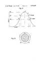
- FIG. 1is a schematic of a pulsed laser system for practicing the invention
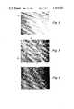
- FIGS. 2 and 3are micrographs of surface portions of silicon wafers that have been annealed using a prior art laser system whereby puddles are formed;
- FIG. 4is a micrograph of a surface portion of a wafer that has been annealed according to this invention whereby no puddle topography is formed;
- FIG. 5is a plot of a typical near-Gaussian energy distribution curve for a laser pulse and its annealing effects on the surface of a semiconductor body for a pulse of laser energy;
- FIG. 6is a cross-sectional view of pulsed beam as seen along viewing plane 6--6 of the beam 16 as shown in FIG. 1, and related to the curve of FIG. 5.
- FIG. 1A schematic of a pulsed laser annealing system embodying the present invention is illustrated in FIG. 1.
- a source of electromagnetic energy radiationsuch as a pulsed laser 12 provides a beam 14 that is optically scanned by a scanner 18 providing a scanned beam 16 impinging on the surface of a body of material, such as a silicon wafer 20, supported in a wafer holder 22.
- the laser beam 14is focused by a lens 24.
- the beam 14 from the laser 12, conveniently termed the primary beam 14,is sampled for control purposes by a beam splitter 26.
- Splitter 26provides a sampled beam 28 of about 5% of the total beam energy which sampled beam 28 is coupled to a thermopile laser power meter head 30 which in turn provides a signal coupled to a calibrated meter 32 for indicating the power of the laser beam 14.
- the optical scanner 18is suitably formed of a pair of mirrors 34 and 36 that are mounted to be driven by a galvanometer 38 and a galvanometer 40, respectively.
- the mirrors 34 and 36are dielectric-coated for near-100% reflection and are arranged along the output optics of the pulsed laser 12 so as to effect x and y scanning deflections of the beam 14 to the surface of the wafer 20 as the reflected beam 16.
- the beam 16is thus deflected in an x and y raster scan similar to a TV-raster.
- the galvanometers 38 and 40are driven by a suitable saw tooth signal from a source 41 to effect the desired scanning.
- the oscillatory motion of the mirrorscan be accurately controlled with different voltage waveforms such as a saw tooth or ramp signal with adjustable periodicity and amplitude in a manner as well known in the art. Accordingly, adjustment on the amount of overlapping that occurs between adjacent pulse spots from the beam 16 onto the target wafer 20 can be provided as desired.
- the target wafer 20is located about two meters from the optical scanner mirrors 34 and 36 to minimize variations in the angle of incidence at different locations on the wafer, which is typically of about 3" (7.5 cm.) in diameter.
- Uniformity of annealingis achieved by scanning the laser beam 16 over the surface of the wafer with at least a 50% overlap between adjacent pulses.
- the laser pulsed energyis desirably quite stable whereby annealing can be achieved with reasonable reproducibility.
- the wafer throughputfor example, of 3" (7.5 cm) diameter wafers, is also predictably quite high, for example in the order of 20 to 60 wafers/hour. Accordingly, the embodiment of the invention being described is capable of handling production quantity wafers.
- the laser 12provides a pulsed beam of electromagnetic optical radiation having sufficient energy to cause the material of the wafer 20 to be annealed by activity of electrons derived principally from the energy conversion of the radiation photons and, moreover, with much less contribution from any atomic motion activity inherent in the material.
- This photon-derived electron activityeffects the annealing process which converts the material into crystalline form by breaking the covalent bonds of the constituents of the material and allowing them to reform into a lattice of essentially single crystalline form.
- the photon-derived electronsare components of a plasma comprising electron-hole pairs generated by the photo-energy conversion process. This annealing plasma is known in the art as pulsed plasma annealing (PPA) as mentioned hereinabove.
- PPApulsed plasma annealing
- annealingis accomplished by the pulsed generation of a very high density plasma within the material, resulting in the breakage of almost all the covalent bonds so that the properties of the material resembles those of a liquid but with the physical temperature of the material during this exposure to the pulsed beam far below the normal melting point of the material.
- This mechanismis in contrast to the annealing process developed by purely thermal mechanisms, i.e. mechanisms of the motion of the atomic particles of the material.
- the wavelength of the laser beam as well as the pulse width of the beamdetermine whether thermal annealing or pulse plasma annealing will be the dominant mechanism.
- the problem that has been prevailing in the prior art of undesirable melting of the material during annealing causing the puddle effecthas been due to thermal annealing phenomenon.
- the problem of this melting effect causing, that which is sometimes termed, puddle topographyis overcome by certain conditions that must be met.
- Micrographs of puddle topographyare shown in FIGS. 2 and 3 to be described hereinafter.
- the conditions to overcome the puddle topography in annealing siliconcomprise: first, the wavelength of the laser for silicon material must be equal to or less than 0.6 micrometer. This value of 0.6 micrometer has been determined by me both empirically and experimentally in relation to the absorption characteristics of silicon. The wavelength must be sufficiently small so that the energy absorption is confined to the surface layer consisting of covalent bonded material. If the wavelength is greater than 0.6 ⁇ m, the absorption depth would be too deep to develop a dense plasma.
- the photon energyshould be at least twice the value of the band gap energy in order for the photons to be adequately absorbed near the surface of the material. If the photon energy is less than the band gap energy, there would be no absorption of the photon energy and the material would thus be transparent to the beam.
- equations (1) and (2)can be modified as follows:
- the wavelength of the laser beamis thus related to the absorption of the photon energy by the material as a function of the band gap energy and is thus used as a criterion to determine the thickness of the surface layer that is to be annealed.
- the pulse width of the laser beam 16must be equal to or less than 50 nanoseconds.
- the pulse widthdetermines the amount of time that the laser beam is impinging on the surface of the material and thus affects the amount of energy per unit time that is imparted to the material. If the time period is too long, the thermal effect, again, will be stimulated to cause the undesirable melting.
- the pulse width of each pulse of radiation energymust be of such short duration as to reduce, if not minimize, the diffusion depth of electrons and holes in the material so that a high enough plasma density can be achieved in the surface layer of the material.
- the diameter of the beammust be significantly greater that the desired depth of the material to be annealed to obviate convection flow of the material during the annealing process. It should be understood that the convective flow occurs in the prior art annealing processes whereby the puddle topology is caused by the thermal annealing processes discussed above. In the embodiment being described, the beam diameter was determined to be on the order of 5.0 mm.
- the scanning rate of the systemwill be based on the desired throughput, that is, the number of wafers that are to be processed per hour as well as the amount of overlap that is to be provided to achieve uniform exposure.
- Uniform exposureis achieved according to the criterion of at least 50% overlap of each pulse relative to the previous pulse.
- the amount of overlapis determined by the exposed area of the surface material actually exposed to the beam. This will be explained in further detail with respect to FIGS. 5 and 6.
- the annealing effect of each pulseis independent of the effect of every other pulse that has occurred. The reason for this is that the annealing effects of each pulse is short ( ⁇ 100 ns) compared to the separation of the pulses (1.0 sec.). It should be understood further that as the amount of overlap is extended from the minimum of 50% to a maximum of 100% no scanning will be effected since a 100% overlap means, obviously, no movement of the beam. Accordingly, the scanning rate is a function of the maximum possible throughput but with uniform exposure. Once the material has been converted to a crystalline state additional or further annealing will not affect the crystalline state of the material.
- a pulsed laser system used to anneal a semiconductor wafer formed of silicon and having a diameter of 3" (7.5 cm)would have the following specifications:
- the wavelength to provide adequate absorption in siliconwould be 0.53 ⁇ m.
- the powershould be about 0.6 joule/cm 2 with a pulse width of about 15 nanoseconds for each pulse.
- the scannershould move the beam 16 over a 3" diameter wafer with about a 50% overlap between adjacent pulses in about one to two minutes.
- a commercially available laser systemthat satisfies the requirements adequately, is manufactured by the Molectron Corporation, as its Model MY34. It is a pulsed Nd:YAG laser. This laser achieves the desired high pulse energy output with a near Gaussian beam intensity profile by utilizing what is known as a polarization-coupled "unstable resonator" technique.
- an unstable resonatoris one in which polarizers of the laser resonator are coupled to inhibit certain modes of resonance.
- the nominal laser beam diameter of the systemis 8 mm with a pulse width of 15-30 nanoseconds and a pulse energy at 1.06 ⁇ m of 700 milli-joules.
- the output beamis converted to the required 0.53 ⁇ m wavelength needed for adequate absorption in the silicon by passing the primary radiation through a second harmonic generator which consists of a KD*P crystal (a crystal formed of potassium dideuterium phosphate).
- This crystal with suitable frequency doubling and filtering meansas known in the art provides means to double the frequency and thus half the wavelength of the laser beam.
- Such a meansis shown in FIG. 1 as filtering mechanism 42 of the laser 12.
- the conversion efficiency of mechanism 42is about 30%.
- the 1.06 ⁇ m component of the laser beamis either dumped into a so-called "beam dump" of known form or brought out coaxially with the beam component at 0.53 ⁇ m wavelength.
- the laser beam 14is suitably pulsed at 10-20 pulses/second (pps) with a pulsed energy stability of ⁇ 2% for the 1.06 ⁇ m component and ⁇ 4% for the 0.53 ⁇ m component.
- An ideal systemis one having a 5 inch (12.7 cm) uniform intensity beam with wavelength and power requirements as outlined above. Unfortunately, such a system does not now exist to my knowledge.
- FIG. 5shows, a typical Gaussian distribution curve 43 as used in the art of the relative intensity of one pulse of the beam 16 irradiating surface of the wafer 20 and to FIG. 6 showing the cross section of the beam 16 taken at viewing line 6--6 in FIG. 1.
- the beam energy not being uniform throughoutis represented by a more intense central region 16a and a less intense region 16b in the peripheral region, as seen in FIG. 6, correlated to the cross-sectional view of the beam 16 in FIG. 5 by the dotted lines.
- the Gaussian distribution curve 43is related to beam region 16a by the threshold value at points 44 and 46, respectively, of the curve 43 at about 75% of the maximum value or peak value 45 of the curve 43.
- the so-called half power pointsare at points 48 and 50 related to the peripheral region 16b of the beam 16.
- the inner portion of the beam 16ais the beam portion that achieves the desired PPA effect.
- the peripheral region 16bwill not provide the desired PPA effect. Accordingly, as the beam 16 is scanned across the surface, it is essential that the portion 16a of each pulse of the beam be overlapped with subsequent beam positions to assure the PPA effect.
- a wafer 20 after ion implantationwas placed in position on holder 22 and then scanned by the laser beam 16. Wafer 20 was restored to its original crystalline state without any puddles appearing on the wafer surface. This was confirmed by a Nomarsky micrograph as illustrated in FIG. 4.
- the micrograph of FIG. 4was made of a bulk silicon wafer 20 that was initially implanted with arsenic ions ( 75 As + ), at 180 kiloelectron volts (KeV), with a dose of 1 ⁇ 10 15 /cm 2 , thereby damaging the original crystalline quality of the wafer material.
- the wafer 20was completely annealed with the pulse laser 10 operated in the frequency-doubled mode with an output of 0.53 ⁇ m, a pulse width of 15 nanoseconds and a repetition rate of 10 pulses/second.
- the micrograph of FIG. 4is virtually black indicating no reflections since there are no discernable features of topography. Note the sharp contrast with a silicon wafer that had extreme puddle topology, as shown in the micrographs of FIGS. 2 and 3 now to be described further.
- FIG. 2illustrating one example of puddle topography developed on a wafer.
- the micrographwas made with a microscope with 500x magnification.
- the laser usedwas a frequency-doubled Nd:YAG laser providing a beam at a wavelength of 0.53 ⁇ m, a diameter of about 40 ⁇ m and a pulse width of 150 nanoseconds.
- the pulse energywas 2J/cm 2 .
- the puddle topographyis seen by the rings 60 which occur in some peripheral portion of each beam pulse depending on the beam intensity profile (similar to FIG. 5 described above). The puddle topography is caused primarily because the pulse width was too long and beam diameter was too small.
- the micrograph shown in FIG. 3was made with a 15x microscope.
- the laser usedwas the Molectron Model MY34 described above but operated with a set of conditions different from that required by this invention as follows:
- the beamhad a diameter of about 3 mm, a wavelength of 1.06 ⁇ m, a pulse width of 15 ns and a per pulse energy of 1J/cm 2 .
- the implanted dopant ( 75 AS 30 at 180 KeV 10 15 /cm -2 )in the silicon waferwas incompletely activated as indicated by resistivity measurements.
- the irregular rings 62 distributed over the wafer surfaceindicate the puddle topography that developed after annealing the ion-implanted wafer with the laser operating at the conditions just stated.
- the wavelength at 1.06 ⁇ mwas too long thus causing the puddles.
- FIGS. 2 and 3should again be contrasted with the puddle-free micrograph of FIG. 4, described above, made according to the present invention.
- the uniformity in annealing by the laser annealing system and method of the inventionwas evaluated by a two point probe, spreading resistivity measurement across two orthogonal diameters of a three inch (7.67 cm) wafer that had been first ion-implanted and subsequently scan laser annealed according to the invention. The results of such an evaluation indicated that reasonably good uniformity had been achieved.
- the material used in the embodiment describedwas silicon, it appears that germanium could be annealed by the process. If germanium is used, the wavelength of the laser would preferably be ⁇ 1 ⁇ m.
- the inventioncan be used to anneal amorphous silicon or polycrystalline silicon material.
- the non-crystalline materialis converted into a single crystalline layer of material.
- the annealing processis otherwise the same described hereinabove.
- metalssuch as copper, aluminum and the like and other elements such as boron, carbon and the like, could be annealed according to the principles of this invention to convert covalent bonded atoms or molecules into single crystal or essentially single crystalline form.
Landscapes
- Physics & Mathematics (AREA)
- Engineering & Computer Science (AREA)
- High Energy & Nuclear Physics (AREA)
- Optics & Photonics (AREA)
- Health & Medical Sciences (AREA)
- Toxicology (AREA)
- Electromagnetism (AREA)
- Condensed Matter Physics & Semiconductors (AREA)
- General Physics & Mathematics (AREA)
- Manufacturing & Machinery (AREA)
- Computer Hardware Design (AREA)
- Microelectronics & Electronic Packaging (AREA)
- Power Engineering (AREA)
- Recrystallisation Techniques (AREA)
Abstract
Description
E.sub.ph =hc/λ (1)
E.sub.ph ˜2E.sub.g (2)
λ≲1.237/2E.sub.g (3)
Claims (7)
Priority Applications (1)
| Application Number | Priority Date | Filing Date | Title |
|---|---|---|---|
| US06/342,473US4439245A (en) | 1982-01-25 | 1982-01-25 | Electromagnetic radiation annealing of semiconductor material |
Applications Claiming Priority (1)
| Application Number | Priority Date | Filing Date | Title |
|---|---|---|---|
| US06/342,473US4439245A (en) | 1982-01-25 | 1982-01-25 | Electromagnetic radiation annealing of semiconductor material |
Publications (1)
| Publication Number | Publication Date |
|---|---|
| US4439245Atrue US4439245A (en) | 1984-03-27 |
Family
ID=23341981
Family Applications (1)
| Application Number | Title | Priority Date | Filing Date |
|---|---|---|---|
| US06/342,473Expired - LifetimeUS4439245A (en) | 1982-01-25 | 1982-01-25 | Electromagnetic radiation annealing of semiconductor material |
Country Status (1)
| Country | Link |
|---|---|
| US (1) | US4439245A (en) |
Cited By (48)
| Publication number | Priority date | Publication date | Assignee | Title |
|---|---|---|---|---|
| US4522656A (en)* | 1983-07-07 | 1985-06-11 | Wacker-Chemitronic Gesellschaft Fur Elektronik-Grundstoffe Mbh | Method of making reference surface markings on semiconductor wafers by laser beam |
| US4556524A (en)* | 1981-11-10 | 1985-12-03 | The Secretary Of State For Defence In Her Britannic Majesty's Government Of The United Kingdom Of Great Britain And Northern Ireland | Method for preparing digital storage device by laser application |
| US4710477A (en)* | 1983-09-12 | 1987-12-01 | Hughes Aircraft Company | Method for forming latch-up immune, multiple retrograde well high density CMOS FET |
| US5094977A (en)* | 1991-01-25 | 1992-03-10 | Micron Technology, Inc. | Stress reduction in metal films by laser annealing |
| US5328855A (en)* | 1991-07-25 | 1994-07-12 | Matsushita Electric Industrial Co., Ltd. | Formation of semiconductor diamond |
| US5365875A (en)* | 1991-03-25 | 1994-11-22 | Fuji Xerox Co., Ltd. | Semiconductor element manufacturing method |
| US5366926A (en)* | 1993-06-07 | 1994-11-22 | Xerox Corporation | Low temperature process for laser dehydrogenation and crystallization of amorphous silicon |
| US5372836A (en)* | 1992-03-27 | 1994-12-13 | Tokyo Electron Limited | Method of forming polycrystalling silicon film in process of manufacturing LCD |
| US5432122A (en)* | 1992-11-03 | 1995-07-11 | Gold Star Co., Ltd. | Method of making a thin film transistor by overlapping annealing using lasers |
| US5529951A (en)* | 1993-11-02 | 1996-06-25 | Sony Corporation | Method of forming polycrystalline silicon layer on substrate by large area excimer laser irradiation |
| US5604635A (en)* | 1995-03-08 | 1997-02-18 | Brown University Research Foundation | Microlenses and other optical elements fabricated by laser heating of semiconductor doped and other absorbing glasses |
| US5643801A (en)* | 1992-11-06 | 1997-07-01 | Semiconductor Energy Laboratory Co., Ltd. | Laser processing method and alignment |
| US5768022A (en)* | 1995-03-08 | 1998-06-16 | Brown University Research Foundation | Laser diode having in-situ fabricated lens element |
| US5919607A (en)* | 1995-10-26 | 1999-07-06 | Brown University Research Foundation | Photo-encoded selective etching for glass based microtechnology applications |
| US5960323A (en)* | 1996-06-20 | 1999-09-28 | Sanyo Electric Co., Ltd. | Laser anneal method for a semiconductor device |
| US6054739A (en)* | 1994-12-16 | 2000-04-25 | Semiconductor Energy Laboratory Co., Ltd. | Semiconductor device having channel refractive index in first and second directions |
| US6136632A (en)* | 1995-12-26 | 2000-10-24 | Seiko Epson Corporation | Active matrix substrate, method of producing an active matrix substrate, liquid crystal display device, and electronic equipment |
| US6160827A (en)* | 1997-02-28 | 2000-12-12 | Semiconductor Energy Laboratory, Co., Ltd. | Laser irradiating device and laser irradiating method |
| US6204099B1 (en) | 1995-02-21 | 2001-03-20 | Semiconductor Energy Laboratory Co., Ltd. | Method for producing insulated gate thin film semiconductor device |
| US6297135B1 (en) | 1997-01-29 | 2001-10-02 | Ultratech Stepper, Inc. | Method for forming silicide regions on an integrated device |
| US20010036755A1 (en)* | 2000-04-28 | 2001-11-01 | Koichiro Tanaka | Method of fabricating semiconductor device |
| US6387803B2 (en) | 1997-01-29 | 2002-05-14 | Ultratech Stepper, Inc. | Method for forming a silicide region on a silicon body |
| US6410374B1 (en) | 1992-12-26 | 2002-06-25 | Semiconductor Energy Laborartory Co., Ltd. | Method of crystallizing a semiconductor layer in a MIS transistor |
| US6423605B1 (en)* | 2000-11-09 | 2002-07-23 | Gyrotron Technology, Inc. | Method and apparatus for forming ultra-shallow junction for semiconductor device |
| US20020114745A1 (en)* | 2001-01-08 | 2002-08-22 | Elliott David J. | Photocatalytic reactor system for treating flue effluents |
| EP1083590A4 (en)* | 1999-03-05 | 2002-09-18 | Seiko Epson Corp | METHOD FOR PRODUCING A THIN-LAYER SEMICONDUCTOR COMPONENT |
| US20030060026A1 (en)* | 1995-07-25 | 2003-03-27 | Semiconductor Energy Laboratory Co. Ltd., A Japanese Corporation | Laser annealing method and apparatus |
| US6544825B1 (en) | 1992-12-26 | 2003-04-08 | Semiconductor Energy Laboratory Co., Ltd. | Method of fabricating a MIS transistor |
| US6577386B2 (en)* | 1997-11-28 | 2003-06-10 | Matsushita Electric Industrial Co., Ltd. | Method and apparatus for activating semiconductor impurities |
| US6680460B1 (en)* | 1999-08-16 | 2004-01-20 | Nec Corporation | Apparatus for producing a semiconductor thin film |
| US20040209410A1 (en)* | 2003-04-21 | 2004-10-21 | Semiconductor Energy Laboratory Co., Ltd. | Beam irradiation apparatus, beam irradiation method, and method for manufacturing thin film transistor |
| US20040241923A1 (en)* | 2003-05-26 | 2004-12-02 | Fuji Photo Film Co., Ltd. | Laser annealing apparatus and laser annealing method |
| US20040253839A1 (en)* | 2003-06-11 | 2004-12-16 | Tokyo Electron Limited | Semiconductor manufacturing apparatus and heat treatment method |
| US20050037552A1 (en)* | 2003-04-21 | 2005-02-17 | Semiconductor Energy Laboratory Co., Ltd. | Beam irradiation apparatus, beam irradiation method, and method for manufacturing semiconductor device |
| US6900121B1 (en)* | 2002-03-14 | 2005-05-31 | Advanced Micro Devices, Inc. | Laser thermal annealing to eliminate oxide voiding |
| EP1538676A1 (en) | 1993-10-20 | 2005-06-08 | Sel Semiconductor Energy Laboratory Co., Ltd. | Thin film semiconductor integrated circuit and method of fabricating the same |
| KR100506956B1 (en)* | 1996-02-15 | 2005-11-28 | 가부시키가이샤 한도오따이 에네루기 켄큐쇼 | Semiconductor device formation method and semiconductor device manufacturing method |
| US20050277028A1 (en)* | 2001-10-30 | 2005-12-15 | Semiconductor Energy Laboratory Co., Ltd. | Laser apparatus, laser irradiation method, manufacturing method for semiconductor device, semiconductor device, production system for semiconductor device using the laser apparatus, and electronic equipment |
| US20060128073A1 (en)* | 2004-12-09 | 2006-06-15 | Yunlong Sun | Multiple-wavelength laser micromachining of semiconductor devices |
| US20070000428A1 (en)* | 2001-11-27 | 2007-01-04 | Semiconductor Energy Laboratory Co., Ltd. | Laser irradiation apparatus |
| US20070141817A1 (en)* | 2004-09-21 | 2007-06-21 | Atmel Corporation | Non-thermal annealing of doped semiconductor material |
| US20070207612A1 (en)* | 2003-10-01 | 2007-09-06 | Yoo Woo S | Selective heating using flash anneal |
| US20070212859A1 (en)* | 2006-03-08 | 2007-09-13 | Paul Carey | Method of thermal processing structures formed on a substrate |
| US7270724B2 (en) | 2000-12-13 | 2007-09-18 | Uvtech Systems, Inc. | Scanning plasma reactor |
| US20080025354A1 (en)* | 2006-07-31 | 2008-01-31 | Dean Jennings | Ultra-Fast Beam Dithering with Surface Acoustic Wave Modulator |
| US20090032511A1 (en)* | 2007-07-31 | 2009-02-05 | Adams Bruce E | Apparatus and method of improving beam shaping and beam homogenization |
| US7548364B2 (en) | 2006-07-31 | 2009-06-16 | Applied Materials, Inc. | Ultra-fast beam dithering with surface acoustic wave modulator |
| US20160379830A1 (en)* | 2015-06-29 | 2016-12-29 | International Business Machines Corporation | Multiple nanosecond laser pulse anneal processes and resultant semiconductor structure |
Citations (5)
| Publication number | Priority date | Publication date | Assignee | Title |
|---|---|---|---|---|
| US4059461A (en)* | 1975-12-10 | 1977-11-22 | Massachusetts Institute Of Technology | Method for improving the crystallinity of semiconductor films by laser beam scanning and the products thereof |
| US4187126A (en)* | 1978-07-28 | 1980-02-05 | Conoco, Inc. | Growth-orientation of crystals by raster scanning electron beam |
| US4234356A (en)* | 1979-06-01 | 1980-11-18 | Bell Telephone Laboratories, Incorporated | Dual wavelength optical annealing of materials |
| US4309225A (en)* | 1979-09-13 | 1982-01-05 | Massachusetts Institute Of Technology | Method of crystallizing amorphous material with a moving energy beam |
| US4315130A (en)* | 1978-03-03 | 1982-02-09 | Hitachi, Ltd. | Method of treating object by laser beam and apparatus therefor |
- 1982
- 1982-01-25USUS06/342,473patent/US4439245A/ennot_activeExpired - Lifetime
Patent Citations (5)
| Publication number | Priority date | Publication date | Assignee | Title |
|---|---|---|---|---|
| US4059461A (en)* | 1975-12-10 | 1977-11-22 | Massachusetts Institute Of Technology | Method for improving the crystallinity of semiconductor films by laser beam scanning and the products thereof |
| US4315130A (en)* | 1978-03-03 | 1982-02-09 | Hitachi, Ltd. | Method of treating object by laser beam and apparatus therefor |
| US4187126A (en)* | 1978-07-28 | 1980-02-05 | Conoco, Inc. | Growth-orientation of crystals by raster scanning electron beam |
| US4234356A (en)* | 1979-06-01 | 1980-11-18 | Bell Telephone Laboratories, Incorporated | Dual wavelength optical annealing of materials |
| US4309225A (en)* | 1979-09-13 | 1982-01-05 | Massachusetts Institute Of Technology | Method of crystallizing amorphous material with a moving energy beam |
Non-Patent Citations (17)
| Title |
|---|
| "Epitaxial Laser Crystallization of Thin-film Amorphous Silicon" by J. C. Bean et al., Appl. Phys. Lett., 33(3) Aug. 1978, pp. 227-230. |
| "Laser Cold Processing Takes the Heat Off Semiconductors" by R. A. Kaplan et al., Electronics, Feb. 28, 1980, pp. 137-142. |
| "Nonthermal Pulsed Laser Annealing of Si; Plasma Annealing" by J. A. Van Vechten et al., Phys. Lett., Dec. 10, 1979, vol. 74A, No. 6, pp. 422-426. |
| "Reasons to Believe Pulsed Laser Annealing of Si Does Not Involve Simple Thermal Melting" by J. A. Van Vechten et al., Phys. Lett., Dec. 10, 1979, vol. 74A, No. 6, pp. 417-421. |
| "Time-Resolved Raman Scattering and Transmission Measurements During Pulsed Laser Annealing" by A. Compaan et al., Laser and Electron-Beam Solid Interactions and Material Processing, pp. 15-22, Publ. by Elsevier North Holland Inc., 1981. |
| A Manual by Molectron Corp. on ND:YAG Lasers, Printed in USA, May 1979, pp. 1 16.* |
| A Manual by Molectron Corp. on ND:YAG Lasers, Printed in USA, May 1979, pp. 1-16. |
| A Nomarski Micrograph, an Enlarged Copy of FIG. 2 Shown on p. 228 of the Bean et al., Article Citation AR, Supra.* |
| Boston Meeting Symp. Rept., Laser Focus, Jan. 1982, pp. 12, 14, 16 and 18.* |
| Epitaxial Laser Crystallization of Thin film Amorphous Silicon by J. C. Bean et al., Appl. Phys. Lett., 33(3) Aug. 1978, pp. 227 230.* |
| Gibson, J. Vac. Sci. Technol, 18 (1981) 810.* |
| Laser Cold Processing Takes the Heat Off Semiconductors by R. A. Kaplan et al., Electronics, Feb. 28, 1980, pp. 137 142.* |
| Leamy et al., Appl. Phys. Letts. 32 (1978) 535.* |
| Lo et al., Phys. Rev. Letts. 44 (1980) 1604.* |
| Nonthermal Pulsed Laser Annealing of Si; Plasma Annealing by J. A. Van Vechten et al., Phys. Lett., Dec. 10, 1979, vol. 74A, No. 6, pp. 422 426.* |
| Reasons to Believe Pulsed Laser Annealing of Si Does Not Involve Simple Thermal Melting by J. A. Van Vechten et al., Phys. Lett., Dec. 10, 1979, vol. 74A, No. 6, pp. 417 421.* |
| Time Resolved Raman Scattering and Transmission Measurements During Pulsed Laser Annealing by A. Compaan et al., Laser and Electron Beam Solid Interactions and Material Processing, pp. 15 22, Publ. by Elsevier North Holland Inc., 1981.* |
Cited By (100)
| Publication number | Priority date | Publication date | Assignee | Title |
|---|---|---|---|---|
| US4556524A (en)* | 1981-11-10 | 1985-12-03 | The Secretary Of State For Defence In Her Britannic Majesty's Government Of The United Kingdom Of Great Britain And Northern Ireland | Method for preparing digital storage device by laser application |
| US4522656A (en)* | 1983-07-07 | 1985-06-11 | Wacker-Chemitronic Gesellschaft Fur Elektronik-Grundstoffe Mbh | Method of making reference surface markings on semiconductor wafers by laser beam |
| US4710477A (en)* | 1983-09-12 | 1987-12-01 | Hughes Aircraft Company | Method for forming latch-up immune, multiple retrograde well high density CMOS FET |
| US5094977A (en)* | 1991-01-25 | 1992-03-10 | Micron Technology, Inc. | Stress reduction in metal films by laser annealing |
| US5365875A (en)* | 1991-03-25 | 1994-11-22 | Fuji Xerox Co., Ltd. | Semiconductor element manufacturing method |
| US5328855A (en)* | 1991-07-25 | 1994-07-12 | Matsushita Electric Industrial Co., Ltd. | Formation of semiconductor diamond |
| USRE36371E (en)* | 1992-03-27 | 1999-11-02 | Tokyo Electron Limited | Method of forming polycrystalline silicon film in process of manufacturing LCD |
| US5372836A (en)* | 1992-03-27 | 1994-12-13 | Tokyo Electron Limited | Method of forming polycrystalling silicon film in process of manufacturing LCD |
| US5432122A (en)* | 1992-11-03 | 1995-07-11 | Gold Star Co., Ltd. | Method of making a thin film transistor by overlapping annealing using lasers |
| US5891764A (en)* | 1992-11-06 | 1999-04-06 | Semiconductor Energy Laboratory Co., Ltd. | Laser processing apparatus and laser processing process |
| US7179726B2 (en)* | 1992-11-06 | 2007-02-20 | Semiconductor Energy Laboratory Co., Ltd. | Laser processing apparatus and laser processing process |
| US5643801A (en)* | 1992-11-06 | 1997-07-01 | Semiconductor Energy Laboratory Co., Ltd. | Laser processing method and alignment |
| US20030153167A1 (en)* | 1992-11-06 | 2003-08-14 | Semiconductor Energy Laboratory Co., Ltd. | Laser processing apparatus and laser processing process |
| US6638800B1 (en) | 1992-11-06 | 2003-10-28 | Semiconductor Energy Laboratory Co., Ltd. | Laser processing apparatus and laser processing process |
| US7799665B2 (en) | 1992-11-06 | 2010-09-21 | Semiconductor Energy Laboratory Co., Ltd. | Laser processing apparatus and laser processing process |
| US20070141859A1 (en)* | 1992-11-06 | 2007-06-21 | Semiconductor Energy Laboratory Co., Ltd. | Laser processing apparatus and laser processing process |
| US6410374B1 (en) | 1992-12-26 | 2002-06-25 | Semiconductor Energy Laborartory Co., Ltd. | Method of crystallizing a semiconductor layer in a MIS transistor |
| US20030207511A1 (en)* | 1992-12-26 | 2003-11-06 | Semiconductor Energy Laboratory Co., Ltd. | Method of fabricating a MIS transistor |
| US7351615B2 (en) | 1992-12-26 | 2008-04-01 | Semiconductor Energy Laboratory Co., Ltd. | Method of fabricating a MIS transistor |
| US6544825B1 (en) | 1992-12-26 | 2003-04-08 | Semiconductor Energy Laboratory Co., Ltd. | Method of fabricating a MIS transistor |
| US5366926A (en)* | 1993-06-07 | 1994-11-22 | Xerox Corporation | Low temperature process for laser dehydrogenation and crystallization of amorphous silicon |
| EP1538676A1 (en) | 1993-10-20 | 2005-06-08 | Sel Semiconductor Energy Laboratory Co., Ltd. | Thin film semiconductor integrated circuit and method of fabricating the same |
| CN100521118C (en)* | 1993-10-20 | 2009-07-29 | 株式会社半导体能源研究所 | Display device |
| US5529951A (en)* | 1993-11-02 | 1996-06-25 | Sony Corporation | Method of forming polycrystalline silicon layer on substrate by large area excimer laser irradiation |
| US6054739A (en)* | 1994-12-16 | 2000-04-25 | Semiconductor Energy Laboratory Co., Ltd. | Semiconductor device having channel refractive index in first and second directions |
| US6242292B1 (en) | 1994-12-16 | 2001-06-05 | Semiconductor Energy Laboratory Co., Ltd. | Method of producing a semiconductor device with overlapped scanned linear lasers |
| US6613619B2 (en) | 1994-12-16 | 2003-09-02 | Semiconductor Energy Laboratory Co., Ltd. | Semiconductor device and method for producing the same |
| US6274885B1 (en) | 1994-12-16 | 2001-08-14 | Semiconductor Energy Laboratory Co., Ltd. | Active matrix display device with TFTs of different refractive index |
| US6921686B2 (en) | 1995-02-21 | 2005-07-26 | Semiconductor Energy Laboratory Co., Ltd. | Method for producing insulated gate thin film semiconductor device |
| US20060141688A1 (en)* | 1995-02-21 | 2006-06-29 | Semiconductor Energy Laboratory Co., Ltd. | Method for producing insulated gate thin film semiconductor device |
| US7615423B2 (en) | 1995-02-21 | 2009-11-10 | Semiconductor Energy Laboratory Co., Ltd. | Method for producing insulated gate thin film semiconductor device |
| US6709905B2 (en) | 1995-02-21 | 2004-03-23 | Semiconductor Energy Laboratory Co., Ltd. | Method for producing insulated gate thin film semiconductor device |
| US7045403B2 (en) | 1995-02-21 | 2006-05-16 | Semiconductor Energy Laboratory Co., Ltd. | Method for producing insulated gate thin film semiconductor device |
| US6204099B1 (en) | 1995-02-21 | 2001-03-20 | Semiconductor Energy Laboratory Co., Ltd. | Method for producing insulated gate thin film semiconductor device |
| US6265745B1 (en) | 1995-02-21 | 2001-07-24 | Semiconductor Energy Laboratory Co., Ltd. | Method for producing insulated gate thin film semiconductor device |
| US5737126A (en)* | 1995-03-08 | 1998-04-07 | Brown University Research Foundation | Microlenses and other optical elements fabricated by laser heating of semiconductor doped and other absorbing glasses |
| US5768022A (en)* | 1995-03-08 | 1998-06-16 | Brown University Research Foundation | Laser diode having in-situ fabricated lens element |
| US5604635A (en)* | 1995-03-08 | 1997-02-18 | Brown University Research Foundation | Microlenses and other optical elements fabricated by laser heating of semiconductor doped and other absorbing glasses |
| US7303980B2 (en)* | 1995-07-25 | 2007-12-04 | Semiconductor Energy Laboratory Co., Ltd. | Laser annealing method and apparatus |
| US20070141768A1 (en)* | 1995-07-25 | 2007-06-21 | Semiconductor Energy Laboratory Co., Ltd. | Method of laser annealing using linear beam having quasi-trapezoidal energy profile for increased depth of focus |
| US20030060026A1 (en)* | 1995-07-25 | 2003-03-27 | Semiconductor Energy Laboratory Co. Ltd., A Japanese Corporation | Laser annealing method and apparatus |
| US7452788B2 (en) | 1995-07-25 | 2008-11-18 | Semiconductor Energy Laboratory Co., Ltd. | Method of laser annealing using linear beam having quasi-trapezoidal energy profile for increased depth of focus |
| US5919607A (en)* | 1995-10-26 | 1999-07-06 | Brown University Research Foundation | Photo-encoded selective etching for glass based microtechnology applications |
| US6136632A (en)* | 1995-12-26 | 2000-10-24 | Seiko Epson Corporation | Active matrix substrate, method of producing an active matrix substrate, liquid crystal display device, and electronic equipment |
| KR100506956B1 (en)* | 1996-02-15 | 2005-11-28 | 가부시키가이샤 한도오따이 에네루기 켄큐쇼 | Semiconductor device formation method and semiconductor device manufacturing method |
| US6072194A (en)* | 1996-06-20 | 2000-06-06 | Sanyo Electric Co., Ltd. | Laser anneal method for a semiconductor device |
| US5960323A (en)* | 1996-06-20 | 1999-09-28 | Sanyo Electric Co., Ltd. | Laser anneal method for a semiconductor device |
| US6297135B1 (en) | 1997-01-29 | 2001-10-02 | Ultratech Stepper, Inc. | Method for forming silicide regions on an integrated device |
| US6387803B2 (en) | 1997-01-29 | 2002-05-14 | Ultratech Stepper, Inc. | Method for forming a silicide region on a silicon body |
| US6516009B1 (en)* | 1997-02-28 | 2003-02-04 | Semiconductor Energy Laboratory Co., Ltd. | Laser irradiating device and laser irradiating method |
| US6160827A (en)* | 1997-02-28 | 2000-12-12 | Semiconductor Energy Laboratory, Co., Ltd. | Laser irradiating device and laser irradiating method |
| US6577386B2 (en)* | 1997-11-28 | 2003-06-10 | Matsushita Electric Industrial Co., Ltd. | Method and apparatus for activating semiconductor impurities |
| EP1083590A4 (en)* | 1999-03-05 | 2002-09-18 | Seiko Epson Corp | METHOD FOR PRODUCING A THIN-LAYER SEMICONDUCTOR COMPONENT |
| US6573161B1 (en) | 1999-03-05 | 2003-06-03 | Seiko Epson Corporation | Thin film semiconductor device fabrication process |
| US6680460B1 (en)* | 1999-08-16 | 2004-01-20 | Nec Corporation | Apparatus for producing a semiconductor thin film |
| US20100184277A1 (en)* | 2000-04-28 | 2010-07-22 | Semiconductor Energy Laboratory Co., Ltd. | Method of fabricating semiconductor device |
| US20010036755A1 (en)* | 2000-04-28 | 2001-11-01 | Koichiro Tanaka | Method of fabricating semiconductor device |
| US7662677B2 (en) | 2000-04-28 | 2010-02-16 | Semiconductor Energy Laboratory Co., Ltd. | Method of fabricating semiconductor device |
| US7951654B2 (en) | 2000-04-28 | 2011-05-31 | Semiconductor Energy Laboratory Co., Ltd. | Method of fabricating semiconductor device |
| US6423605B1 (en)* | 2000-11-09 | 2002-07-23 | Gyrotron Technology, Inc. | Method and apparatus for forming ultra-shallow junction for semiconductor device |
| US7270724B2 (en) | 2000-12-13 | 2007-09-18 | Uvtech Systems, Inc. | Scanning plasma reactor |
| US6773683B2 (en) | 2001-01-08 | 2004-08-10 | Uvtech Systems, Inc. | Photocatalytic reactor system for treating flue effluents |
| US20020114745A1 (en)* | 2001-01-08 | 2002-08-22 | Elliott David J. | Photocatalytic reactor system for treating flue effluents |
| US7892952B2 (en)* | 2001-10-30 | 2011-02-22 | Semiconductor Energy Laboratory Co., Ltd. | Laser apparatus, laser irradiation method, manufacturing method for semiconductor device, semiconductor device, production system for semiconductor device using the laser apparatus, and electronic equipment |
| US20050277028A1 (en)* | 2001-10-30 | 2005-12-15 | Semiconductor Energy Laboratory Co., Ltd. | Laser apparatus, laser irradiation method, manufacturing method for semiconductor device, semiconductor device, production system for semiconductor device using the laser apparatus, and electronic equipment |
| US8696808B2 (en) | 2001-11-27 | 2014-04-15 | Semiconductor Energy Laboratory Co., Ltd. | Laser irradiation apparatus |
| US20070000428A1 (en)* | 2001-11-27 | 2007-01-04 | Semiconductor Energy Laboratory Co., Ltd. | Laser irradiation apparatus |
| US6900121B1 (en)* | 2002-03-14 | 2005-05-31 | Advanced Micro Devices, Inc. | Laser thermal annealing to eliminate oxide voiding |
| US7915099B2 (en) | 2003-04-21 | 2011-03-29 | Semiconductor Energy Laboratory Co., Ltd. | Beam irradiation apparatus, beam irradiation method, and method for manufacturing semiconductor device |
| US20070196968A1 (en)* | 2003-04-21 | 2007-08-23 | Semiconductor Energy Laboratory Co., Ltd. | Beam irradiation apparatus, beam irradiation method, and method for manufacturing semiconductor device |
| US20040209410A1 (en)* | 2003-04-21 | 2004-10-21 | Semiconductor Energy Laboratory Co., Ltd. | Beam irradiation apparatus, beam irradiation method, and method for manufacturing thin film transistor |
| US7220627B2 (en)* | 2003-04-21 | 2007-05-22 | Semiconductor Energy Laboratory Co., Ltd. | Method for manufacturing a semiconductor device where the scanning direction changes between regions during crystallization and process |
| US20050037552A1 (en)* | 2003-04-21 | 2005-02-17 | Semiconductor Energy Laboratory Co., Ltd. | Beam irradiation apparatus, beam irradiation method, and method for manufacturing semiconductor device |
| US7476629B2 (en) | 2003-04-21 | 2009-01-13 | Semiconductor Energy Laboratory Co., Ltd. | Beam irradiation apparatus, beam irradiation method, and method for manufacturing thin film transistor |
| US20040241923A1 (en)* | 2003-05-26 | 2004-12-02 | Fuji Photo Film Co., Ltd. | Laser annealing apparatus and laser annealing method |
| US20040253839A1 (en)* | 2003-06-11 | 2004-12-16 | Tokyo Electron Limited | Semiconductor manufacturing apparatus and heat treatment method |
| US7507667B2 (en)* | 2003-10-01 | 2009-03-24 | Wafermasters, Inc. | Selective heating using flash anneal |
| US20070207612A1 (en)* | 2003-10-01 | 2007-09-06 | Yoo Woo S | Selective heating using flash anneal |
| US20070141817A1 (en)* | 2004-09-21 | 2007-06-21 | Atmel Corporation | Non-thermal annealing of doped semiconductor material |
| US7569458B2 (en)* | 2004-09-21 | 2009-08-04 | Atmel Corporation | Non-thermally annealed doped semiconductor material and methods related thereto |
| US20060128073A1 (en)* | 2004-12-09 | 2006-06-15 | Yunlong Sun | Multiple-wavelength laser micromachining of semiconductor devices |
| US20070221640A1 (en)* | 2006-03-08 | 2007-09-27 | Dean Jennings | Apparatus for thermal processing structures formed on a substrate |
| US20070218644A1 (en)* | 2006-03-08 | 2007-09-20 | Applied Materials, Inc. | Method of thermal processing structures formed on a substrate |
| US20070212859A1 (en)* | 2006-03-08 | 2007-09-13 | Paul Carey | Method of thermal processing structures formed on a substrate |
| US20100323532A1 (en)* | 2006-03-08 | 2010-12-23 | Paul Carey | Method of thermal processing structures formed on a substrate |
| US10840100B2 (en) | 2006-03-08 | 2020-11-17 | Applied Materials, Inc. | Method of thermal processing structures formed on a substrate |
| US7569463B2 (en) | 2006-03-08 | 2009-08-04 | Applied Materials, Inc. | Method of thermal processing structures formed on a substrate |
| US10141191B2 (en) | 2006-03-08 | 2018-11-27 | Applied Materials, Inc. | Method of thermal processing structures formed on a substrate |
| TWI463568B (en)* | 2006-03-08 | 2014-12-01 | Applied Materials Inc | Method and apparatus for heat treating a structure formed on a substrate |
| US8518838B2 (en) | 2006-03-08 | 2013-08-27 | Applied Materials, Inc. | Method of thermal processing structures formed on a substrate |
| US7548364B2 (en) | 2006-07-31 | 2009-06-16 | Applied Materials, Inc. | Ultra-fast beam dithering with surface acoustic wave modulator |
| US20080025354A1 (en)* | 2006-07-31 | 2008-01-31 | Dean Jennings | Ultra-Fast Beam Dithering with Surface Acoustic Wave Modulator |
| US8829392B2 (en) | 2007-07-31 | 2014-09-09 | Applied Materials, Inc. | Apparatus and method of improving beam shaping and beam homogenization |
| US8148663B2 (en) | 2007-07-31 | 2012-04-03 | Applied Materials, Inc. | Apparatus and method of improving beam shaping and beam homogenization |
| US9908200B2 (en) | 2007-07-31 | 2018-03-06 | Applied Materials, Inc. | Apparatus and method of improving beam shaping and beam homogenization |
| US20090032511A1 (en)* | 2007-07-31 | 2009-02-05 | Adams Bruce E | Apparatus and method of improving beam shaping and beam homogenization |
| US20160379830A1 (en)* | 2015-06-29 | 2016-12-29 | International Business Machines Corporation | Multiple nanosecond laser pulse anneal processes and resultant semiconductor structure |
| US9859121B2 (en)* | 2015-06-29 | 2018-01-02 | International Business Machines Corporation | Multiple nanosecond laser pulse anneal processes and resultant semiconductor structure |
| US10553439B2 (en)* | 2015-06-29 | 2020-02-04 | International Business Machines Corporation | Multiple nanosecond laser pulse anneal processes and resultant semiconductor structure |
| US11201061B2 (en) | 2015-06-29 | 2021-12-14 | International Business Machines Corporation | Multiple nanosecond laser pulse anneal processes and resultant semiconductor structure |
Similar Documents
| Publication | Publication Date | Title |
|---|---|---|
| US4439245A (en) | Electromagnetic radiation annealing of semiconductor material | |
| US4229232A (en) | Method involving pulsed beam processing of metallic and dielectric materials | |
| US4234358A (en) | Patterned epitaxial regrowth using overlapping pulsed irradiation | |
| US4234356A (en) | Dual wavelength optical annealing of materials | |
| US6051483A (en) | Formation of ultra-shallow semiconductor junction using microwave annealing | |
| US4292093A (en) | Method using laser irradiation for the production of atomically clean crystalline silicon and germanium surfaces | |
| US7772134B2 (en) | Method of annealing using two wavelengths of continuous wave laser radiation | |
| KR101115077B1 (en) | Laser thin film poly-silicon annealing system | |
| KR20070049174A (en) | Laser doping method of solid state material using linear-focused laser beam and method of generating solar-cell emitter based on said method | |
| KR20060126666A (en) | Laser thin film poly-silicon annealing optical system | |
| EP0124261B1 (en) | Process for producing monocrystalline layer on insulator | |
| TW202243786A (en) | Processing device and processing method for solid structure | |
| JP2024038269A (en) | Solid structure processing equipment and processing method | |
| CA1129969A (en) | Dual wavelength optical annealing of materials | |
| Blomberg et al. | Substrate heating effects in CO2 laser annealing of ion‐implanted silicon | |
| Celler et al. | Modification of silicon properties with lasers, electron beams, and incoherent light | |
| JP5610471B2 (en) | Crystal material reforming apparatus and crystal material reforming method | |
| Staggs et al. | Laser Raster Conditioning of KDP and DKDP Crystals using XeCl | |
| JPS6227532B2 (en) | ||
| Klinger et al. | Study of Extended Defect Structure Induced by Pulsed Laser Annealing in Implanted Silicon Crystals | |
| JPS605508A (en) | Manufacture of semiconductor crystal thin film | |
| JPH0352214B2 (en) | ||
| Auleytner et al. | DCXS and RHEED characterization of effectiveness of annealing implanted Si crystals by using pulsed UV excimer laser and sample scanning technique | |
| Merkle et al. | Picosecond Laser Pulse Induced Damage in Crystalline Silicon | |
| JPS6092607A (en) | Electron beam annealing device |
Legal Events
| Date | Code | Title | Description |
|---|---|---|---|
| AS | Assignment | Owner name:RCA CORPORATION, A CORP. OF DE Free format text:ASSIGNMENT OF ASSIGNORS INTEREST.;ASSIGNOR:WU, CHUNG P.;REEL/FRAME:003966/0190 Effective date:19820121 | |
| STCF | Information on status: patent grant | Free format text:PATENTED CASE | |
| CC | Certificate of correction | ||
| FEPP | Fee payment procedure | Free format text:MAINTENANCE FEE REMINDER MAILED (ORIGINAL EVENT CODE: REM.); ENTITY STATUS OF PATENT OWNER: LARGE ENTITY | |
| FEPP | Fee payment procedure | Free format text:SURCHARGE FOR LATE PAYMENT, PL 96-517 (ORIGINAL EVENT CODE: M176); ENTITY STATUS OF PATENT OWNER: LARGE ENTITY | |
| MAFP | Maintenance fee payment | Free format text:PAYMENT OF MAINTENANCE FEE, 4TH YEAR, PL 96-517 (ORIGINAL EVENT CODE: M170); ENTITY STATUS OF PATENT OWNER: LARGE ENTITY Year of fee payment:4 | |
| MAFP | Maintenance fee payment | Free format text:PAYMENT OF MAINTENANCE FEE, 8TH YEAR, PL 96-517 (ORIGINAL EVENT CODE: M171); ENTITY STATUS OF PATENT OWNER: LARGE ENTITY Year of fee payment:8 | |
| MAFP | Maintenance fee payment | Free format text:PAYMENT OF MAINTENANCE FEE, 12TH YEAR, LARGE ENTITY (ORIGINAL EVENT CODE: M185); ENTITY STATUS OF PATENT OWNER: LARGE ENTITY Year of fee payment:12 | |
| FEPP | Fee payment procedure | Free format text:PAYOR NUMBER ASSIGNED (ORIGINAL EVENT CODE: ASPN); ENTITY STATUS OF PATENT OWNER: LARGE ENTITY | |
| AS | Assignment | Owner name:INTERSIL CORPORATION, FLORIDA Free format text:ASSIGNMENT OF ASSIGNORS INTEREST;ASSIGNOR:HARRIS SEMICONDUCTOR PATENTS, INC.;REEL/FRAME:010247/0161 Effective date:19990813 | |
| AS | Assignment | Owner name:CREDIT SUISSE FIRST BOSTON, AS COLLATERAL AGENT, N Free format text:SECURITY INTEREST;ASSIGNOR:INTERSIL CORPORATION;REEL/FRAME:010351/0410 Effective date:19990813 |