US4438354A - Monolithic programmable gain-integrator stage - Google Patents
Monolithic programmable gain-integrator stageDownload PDFInfo
- Publication number
- US4438354A US4438354AUS06/292,870US29287081AUS4438354AUS 4438354 AUS4438354 AUS 4438354AUS 29287081 AUS29287081 AUS 29287081AUS 4438354 AUS4438354 AUS 4438354A
- Authority
- US
- United States
- Prior art keywords
- operational amplifier
- gain
- integrator stage
- input
- capacitor
- Prior art date
- Legal status (The legal status is an assumption and is not a legal conclusion. Google has not performed a legal analysis and makes no representation as to the accuracy of the status listed.)
- Expired - Lifetime
Links
- 239000003990capacitorSubstances0.000claimsabstractdescription102
- 230000000694effectsEffects0.000claimsabstractdescription17
- 230000010354integrationEffects0.000claimsabstractdescription13
- 239000000872bufferSubstances0.000claimsdescription16
- 238000000034methodMethods0.000claimsdescription2
- 230000000903blocking effectEffects0.000description6
- 238000007599dischargingMethods0.000description5
- 238000003491arrayMethods0.000description4
- 238000010586diagramMethods0.000description3
- 230000003071parasitic effectEffects0.000description2
- 238000005070samplingMethods0.000description2
- 230000001052transient effectEffects0.000description2
- 238000005516engineering processMethods0.000description1
- 238000004519manufacturing processMethods0.000description1
- 229910044991metal oxideInorganic materials0.000description1
- 150000004706metal oxidesChemical class0.000description1
- 239000004065semiconductorSubstances0.000description1
Images

Classifications
- H—ELECTRICITY
- H03—ELECTRONIC CIRCUITRY
- H03F—AMPLIFIERS
- H03F1/00—Details of amplifiers with only discharge tubes, only semiconductor devices or only unspecified devices as amplifying elements
- H03F1/30—Modifications of amplifiers to reduce influence of variations of temperature or supply voltage or other physical parameters
- H03F1/303—Modifications of amplifiers to reduce influence of variations of temperature or supply voltage or other physical parameters using a switching device
- H—ELECTRICITY
- H03—ELECTRONIC CIRCUITRY
- H03F—AMPLIFIERS
- H03F3/00—Amplifiers with only discharge tubes or only semiconductor devices as amplifying elements
- H03F3/005—Amplifiers with only discharge tubes or only semiconductor devices as amplifying elements using switched capacitors, e.g. dynamic amplifiers; using switched capacitors as resistors in differential amplifiers
- H—ELECTRICITY
- H03—ELECTRONIC CIRCUITRY
- H03G—CONTROL OF AMPLIFICATION
- H03G3/00—Gain control in amplifiers or frequency changers
- H03G3/001—Digital control of analog signals
Definitions
- This inventionrelates to operational amplifiers and more specifically to a gain-integrator stage utilizing operational amplifiers wherein the effects of the inherent offset voltages of the operational amplifiers contained within the circuit are eliminated. Offset voltages from other causes, including parasitic capacitances, switch operation, and leakage currents, are also eliminated.
- Operational amplifier 115receives input voltage V in from input terminal 111 through a switched capacitor means comprised of switches 112 and 113, and capacitor 114.
- switched capacitorsin this manner is well-known in the prior art. See, for example, an article entitled “Analog Sample Data Filters", IEEE Journal of Solid-Stage Circuits, August 1972, Pg. 302.
- the closed loop gain (G 1 ) of operational amplifier 115is equal to the negative of the ratio of the capacitance of capacitor 114 to the capacitance of capacitor 116, as is well-known.
- the closed loop gain (G 2 ) of operational amplifier 120is equal to the negative of the ratio of the capacitance of capacitor 119 to the capacitance of capacitor 121.
- the overall gain of the circuit of FIG. 1is equal to the product G 1 G 2 .
- capacitors to determine the closed loop gain of an operational amplifieris particularly useful when metal oxide semiconductor (MOS) devices are used as the active elements in the operational amplifier because resistance values, and thus the closed loop gain of an operational amplifier utilizing MOS resistors as the gain determining components, are not highly controllable.
- capacitance valuesare determined by the plate size and the dielectric thickness. Capacitor plate sizes are highly controllable in MOS devices, and dielectric thickness is quite uniform across an MOS device. Thus, capacitance ratios, and therefore the closed loop gain of an operational amplifier using capacitors as shown in FIG. 1, are quite controllable in MOS devices.
- Equation (3)the output voltage at node 151, expressed as a function of the input voltage V in , is shown in Equation (3):
- V out1the output voltage of operational amplifier 115 available at node 150;
- V outthe output voltage of operational amplifier 120 available at node 151;
- G 1the closed loop gain of operational amplifier 115
- G 2the closed loop gain of operational amplifier 120
- V off1the inherent offset voltage of operational amplifier 115
- V off2the inherent offset voltage of operational amplifier 120.
- V errorthe error component of V out .
- V off1 and V off2reduce the dynamic range of the gain-integrator stage of FIG. 1 because the output voltages of operational amplifiers 115 and 120 will saturate at a lower input voltage differential than ideal operational amplifiers free from inherent offset voltages.
- One prior art method of minimizing the effect of the error component, V erroris the use of DC blocking capacitor 122 between node 151 and output terminal 123.
- DC blocking capacitor 122blocks the DC error component V error .
- the use of DC blocking capacitor 122is undesirable because it must be rather large, on the order of approximately 0.1 microfarad, thus resulting in increased cost and the need for an off-chip component if the gain integrator stage is to be formed as an integrated circuit.
- DC blocking capacitor 122effectively blocks all DC components of the output voltage, not just the DC components attributable to offset voltages. Thus, desired DC components of the output voltage are also blocked by DC blocking capacitor 122.
- a unique gain-integrator circuitwherein the closed loop gain of each operational amplifier stage contained therein is programmable by the connection of selected capacitors contained in a capacitor array comprising a plurality of capacitors, thus allowing a wide range of possible gains.
- the circuit of this inventionalso utilizes a unique integrating circuit wherein the amplified input voltages containing offset voltages are alternately integrated with the inverse of the offset voltages, thus providing an integrated output voltage free from the effects of the inherent offset voltages of the operational amplifiers utilized in the circuit, as well as the offset voltages due to parasitic capacitances, leakage currents, and other causes.
- FIG. 1is an example of a prior art gain stage utilizing a DC blocking capacitor to minimize the effects of the inherent offset voltage of the operational amplifiers;
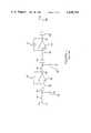
- FIG. 2is a schematic diagram of one embodiment of this invention.
- FIG. 2shows a schematic diagram of this invention.
- gain stages 110 and 120also called “sample and hold stages”
- integrator stage 130to minimize the effect of the inherent offset voltage of the operational amplifier of each stage is given in co-pending U.S. Pat. No. 4,404,525 filed Mar. 3, 1981 and assigned to American Microsystems, Inc., the assignee of this invention, and thus will not be repeated here.
- the contents of aforesaid co-pending United States Patentare hereby incorporated by reference.
- the closed loop gain of gain stage 110is equal to the ratio of the capacitance of the selected capacitors of capacitor array 100 to the capacitance of capacitor 19.
- Selected capacitors of capacitor array 100are connected between input node 271 and inverting input lead 70 of operational amplifier 18.
- the use of capacitor array 100comprised of any desired number of capacitors, allows the gain of sample and hold circuit 110 to be selected from a plurality of possible gains.
- the capacitors of capacitor array 100may be of equal capacitance value or may be binary weighted, wherein the Kth of N capacitors has a capacitance equal to 2 K-1 C, where N is a selected integer and 1 ⁇ K ⁇ N. Any other desired weighting scheme of capacitor array 100 may be utilized as well.
- sample and hold stage 120is identical to the operation of sample and hold circuit 110, thus providing an output voltage V' out at node 170 after one sample of the input voltage has been taken:
- G 1the closed loop gain of sample and hold circuit 110
- G 2the closed loop gain of sample and hold circuit 120
- V in1the first sample of the input voltage applied to terminal 11;
- V off1the offset voltage of sample and hold circuit 110.
- V off2the offset voltage of sample and hold circuit 120.
- gain stages 110 and 120 and integrator stage 130are placed in the unity gain mode to eliminate, or at least minimize, their inherent offset voltages, as described in the previously mentioned co-pending patent.
- any remaining offset voltage (1/A) V off3 of operational amplifier 38(where V off3 is the offset voltage of integrator stage 130, and A is the gain of buffers 46a and 46b) appearing on node 107 is stored in capacitor 45 via closed switch 44.
- Switch 44then opens, thus providing V off3 on output lead 190 of voltage buffer 46a.
- buffer amplifiers 46a and 46bare closely matched, thus providing output voltages substantially equal to V off3 when integrator stage 130 is placed in the unity gain mode.
- integrator stage 130is initialized by discharging integration capacitor 39 in the following manner.
- Switches 34, 35, 37, and 106are opened, thus leaving capacitor 36 disconnected.
- Integrator stage 130is initialized by closing switch 42, thus placing operational amplifier 38, together with buffer amplifier 46b, in the unity gain mode.
- V off3is present on output node 47 and the inverting input lead of operational amplifier 38.
- Switch 41is opened, and switch 40 closed, thus storing V off3 on capacitor 39 connected between the inverting input lead of operational amplifier 38 and ground.
- Switch 44is closed, thus storing (1/A) V off3 on capacitor 45 (where A is the gain of buffers 46a and 46b), thus making V off3 available on output lead 190 of buffer amplifier 46a.
- gain stages 110 and 120are initialized in the same manner as described above with respect to the initialization of integrator stage 130, by opening switches 21 and 22 and closing switches 20, 31, 22 and 33.
- Switch 12opens and switch 13 closes, and switches 15a, 15b, 16a, 16b . . . , 17a, 17b close, thus initializing capacitor array 100 by discharging each capacitor contained within capacitor array 100.
- switch 23opens and switch 24 closes, and switches 26a, 26b, 27a, 27b . . . , 28a, 28b close, thus initializing capacitor array 101 by discharging each capacitor contained within capacitor array 101.
- Dummy switch 57which serves to minimize the offset voltage due to the operation of switch 13 (more fully explained below) opens.
- switches 40 and 42are opened and switch 41 is closed, thus taking integrator stage 130 out of the unity gain mode, and placing integrator stage 130 in the integrating mode.
- Switch 44opens, and (1/A) V off3 remains stored on capacitor 45, and V off3 is available on output lead 190 of buffer amplifier 46a. V off3 is also available on the inverting input lead of operational amplifier 38 because the noninverting input lead of operational amplifier 38 is grounded.
- the gain factor G 1 of gain stage 110is selected by the appropriate connection of selected capacitors within capacitor array 100 between input node 271 and inverting input lead 70 of operational amplifier 18.
- the gain factor G 2 of gain stage 120is selected by the appropriate connection of capacitors of capacitor array 101 between node 371 and the inverting input lead 270 of operational amplifier 29.
- the gain G 1 of gain stage 110is equal to the negative of the ration of the capacitance of capacitor array 100 connected between node 271 and inverting input lead 70 of operational amplifier 18 and the capacitance of capacitor 19.
- the gain G 2 of gain stage 120is equal to the negative of the ratio of the capacitance of capacitor array 101 connected between node 371 and the inverting input lead 270 of operational amplifier 29 and the capacitance of capacitor 30.
- Switches 34 and 37close, thus connecting capacitor 36 between output node 170 of gain stage 120 and the output node 190 of buffer amplifier 46a.
- Switch 13opens and dummy switch 57 closes, thus causing the offset voltage V off1 of gain stage 110 to include a component due to the switching action of switches 13 and 57.
- Switches 12, 13 and 57are closely matched, thus the offset voltage due to the operation of switches 13 and 57 will be substantially equal to the offset voltage due to the operation of switches 12 and 13.
- dummy switch 57allows the offset voltage caused by the operation of switches 12 and 13 (during sampling of the input voltage) to be balanced by the offset voltage caused by the operation of switches 13 and 57 during time T 4 (during sampling of the offset voltage), thereby providing a highly accurate output voltage V out .
- the use of dummy switch 57compensates for the effects of transient signals due to switch operation. This is particularly important at high operating speeds.
- switches 34 and 106open and switches 35 and 37 close, thus connecting capacitor 36 between ground and node 190.
- Thischarges capacitor 36 to (O-V off3 ).
- Switch 23opens, thus disconnecting output node 191 of gain stage 110 from node 371 of gain stage 120.
- Switches 12 and 57open and switch 13 closes, thus removing the input voltage V in from node 271, and discharging (initializing) capacitor array 100.
- Switch 24closes, thus discharging capacitor array 101.
- Switches 20, 22, 31 and 33close and switches 21 and 32 open, thus initializing gain stages 110 and 120.
- switches 35 and 37open and switches 34 and 106 close, thus connecting capacitor 36 between node 170 and the inverting input lead of operational amplifier 38.
- Switch 13opens and switch 12 closes, thus applying the input voltage V in to input node 271 of gain stage 110. This provides G 1 G 2 V in +G 2 V off1 +V off2 on node 170, thus charging capacitor 36 to G 1 G 2 V in +G 2 V off1 +V off2 -V off3 .
- Switches 20, 22, 31 and 33open, and switches 21 and 32 close, thus taking gain stages 110 and 120 out of the initialization mode.
- Switch 23closes and switch 24 opens, thus connecting output node 191 of gain stage 110 to input node 371 of gain stage 120.
- Steps T 3 through T 7are now repeated in sequence, thus integrating the sampled input voltage V in (N).
- V in (N)the sampled input voltage
- -(G 2 V off1 +V off2 )is integrated on capacitor 39.
- T 7(G 1 G 2 V in (N)+G 2 V off1 +V off2 ) is integrated on integration capacitor 39 of integrator stage 130.
- V out (N)the output voltage on terminal 47 after N complete integration cycles
- V off1the offset voltage of sample and hold circuit 110
- V off2the offset voltage of sample and hold circuit 120
- G 1 (K)the closed loop gain of operational amplifier 110 during the Kth integration cycle
- G 2 (K)the closed loop gain of operational amplifier 120 during the Kth integration cycle
- V in (K)the input voltage on terminal 11 during the Kth integration cycle.
- Steps T 3 -T 7are repeated for each sample of input voltage V in , thus providing an integrated output voltage V out which is free from the effects of the inherent offset voltages of operational amplifier 18, 29, and 38.
- the gain G 1 of gain stage 110 and the gain G 2 of gain stage 120may be selected prior to the receipt of each input voltage sample. In this manner, the gain factor of each input voltage sample may be selected independently from the gain factor used in conjunction with other input voltage samples.
- a switched capacitor gain stage utilizing a capacitor arraymay be programmed to one of a plurality of desired gains. Furthermore, the effects of the inherent offset voltages of the operational amplifiers used in the circuit are eliminated.
Landscapes
- Engineering & Computer Science (AREA)
- Power Engineering (AREA)
- Amplifiers (AREA)
- Analogue/Digital Conversion (AREA)
Abstract
Description
V.sub.out1 =G.sub.1 V.sub.in +V.sub.off1 ( 1)
V.sub.out =G.sub.2 V.sub.out1 +V.sub.off2 ( 2)
V.sub.out =G.sub.1 G.sub.2 V.sub.in +G.sub.2 V.sub.off1 +V.sub.off2 ( 3)
V.sub.error =G.sub.2 V.sub.off1 +V.sub.off2 ( 4)
V'.sub.out =G.sub.1 G.sub.2 V.sub.in1 +G.sub.2 V.sub.off1 +V.sub.off2
V'.sub.out =G.sub.2 V.sub.off1 +V.sub.off2.
TABLE I ______________________________________ Time Events Comments ______________________________________ T.sub.0 Switches open: 41, 34, 35,37, 106 Initialize integrator stage 130 Switches close: 40, 42, 44 T.sub.1 Switches open: 12, 23, 21, Initialize gain stages 32, 57 110, 120 and100, 101 Switches close: 13, 24, 20, 31, 22, 33 T.sub.2 Switches open: 40, 42, 44 V.sub.off3 available on Switches close: 41 capacitor arrays node 190.Integration stage 130 in integration mode T.sub.3 Switches within capacitor Select gain factors G.sub.1100 and 101 operate and G.sub.2 via arrays 100 and 101 T.sub.4 Switches open: 24, 20, 31, Store G.sub.2 V.sub.off1 + 13, 22, 33 V.sub.off2 - V.sub.off3 on Switches close: 23, 34, 37, capacitor arrays capacitor 36 21, 32, 57 T.sub.5 Switches open: 34, 37 Store (0 - V.sub.off3) on Switches close: 35, 106capacitor 36, thereby integrating -(G.sub.2 V.sub.off1 + V.sub.off2) oncapacitor 39 T.sub.6 Switches open: 34, 106, 23, Store (0 - V.sub.off3) on 57, 12, 21, 32capacitor 36. Initial- Switches close: 35, 37, 13, 22, ize gain stages 110, 33, 31, 20, 24 120 and110, 101 T.sub.7 Switches open: 13, 35, 37, 22, Store (G.sub.1 G.sub.2 V.sub.in + 33, 20. 31, 24 G.sub.2 V.sub.off1 + V.sub.off2) - Switches close: 12, 34, 106, V.sub.off3 on capacitor arrays 36, 21, 32, 23 thereby integrating G.sub.1 G.sub.2 V.sub.in + G.sub.2 V.sub.off1 + V.sub.off2 on capacitor capacitor 39. Total charge stored oncapacitor 39 from steps T.sub.5 and T.sub.7 is equal to G.sub.1 G.sub.2 V.sub.in Repeat steps T.sub.3 -T.sub.7 until integrator stage is to be reinitialized. For reinitialization of integrator stage, begin at step T.sub.0. ______________________________________
Claims (10)
Priority Applications (5)
| Application Number | Priority Date | Filing Date | Title |
|---|---|---|---|
| US06/292,870US4438354A (en) | 1981-08-14 | 1981-08-14 | Monolithic programmable gain-integrator stage |
| JP57136427AJPS5840686A (en) | 1981-08-14 | 1982-08-06 | Monolithic programable gain-integrator |
| EP82401498AEP0072741B1 (en) | 1981-08-14 | 1982-08-06 | Programmable gain integrator stage including means for offset voltage elimination |
| DE8282401498TDE3274706D1 (en) | 1981-08-14 | 1982-08-06 | Programmable gain integrator stage including means for offset voltage elimination |
| CA000408939ACA1187950A (en) | 1981-08-14 | 1982-08-06 | Monolithic programmable gain-integrator stage |
Applications Claiming Priority (1)
| Application Number | Priority Date | Filing Date | Title |
|---|---|---|---|
| US06/292,870US4438354A (en) | 1981-08-14 | 1981-08-14 | Monolithic programmable gain-integrator stage |
Publications (1)
| Publication Number | Publication Date |
|---|---|
| US4438354Atrue US4438354A (en) | 1984-03-20 |
Family
ID=23126569
Family Applications (1)
| Application Number | Title | Priority Date | Filing Date |
|---|---|---|---|
| US06/292,870Expired - LifetimeUS4438354A (en) | 1981-08-14 | 1981-08-14 | Monolithic programmable gain-integrator stage |
Country Status (5)
| Country | Link |
|---|---|
| US (1) | US4438354A (en) |
| EP (1) | EP0072741B1 (en) |
| JP (1) | JPS5840686A (en) |
| CA (1) | CA1187950A (en) |
| DE (1) | DE3274706D1 (en) |
Cited By (62)
| Publication number | Priority date | Publication date | Assignee | Title |
|---|---|---|---|---|
| US4529965A (en)* | 1983-05-03 | 1985-07-16 | Racal Data Communications | Switched-capacitor circuit analog-to-digital converter |
| US4555668A (en)* | 1983-10-14 | 1985-11-26 | American Microsystems, Inc. | Gain amplifier |
| US4988900A (en)* | 1988-12-28 | 1991-01-29 | Sgs-Thomson Microelectronics S.A. | Analog signal waveform generator |
| US5121008A (en)* | 1990-11-29 | 1992-06-09 | Talmadge Paul C | Circuit for generating or demodulating a square wave and other wave forms |
| US5168179A (en)* | 1988-11-04 | 1992-12-01 | Silicon Systems, Inc. | Balanced modulator for auto zero networks |
| US5182521A (en)* | 1987-08-28 | 1993-01-26 | The University Of Melbourne | Time-multiplexed switched capacitor circuit having reduced capacitance |
| US5281860A (en)* | 1991-07-26 | 1994-01-25 | Texas Instruments Incorporated | Method and apparatus for an improved multiple channel sensor interface circuit |
| US5289332A (en)* | 1990-09-21 | 1994-02-22 | France Telecom Etablissement Autonome De Droit Public (Centre National D'etudes Des Telecommunications) | Protective circuit for a control circuit, in particular of liquid crystal display screen |
| US5327098A (en)* | 1993-07-29 | 1994-07-05 | Burr-Brown Corporation | Programmable gain amplifier circuitry and method for biasing JFET gain switches thereof |
| US5391999A (en)* | 1993-12-02 | 1995-02-21 | Motorola Inc. | Glitchless switched-capacitor biquad low pass filter |
| EP0653855A1 (en)* | 1993-11-11 | 1995-05-17 | Motorola, Inc. | A differential switched capacitor circuit |
| US5457417A (en)* | 1993-02-05 | 1995-10-10 | Yozan Inc. | Scaler circuit |
| US5585756A (en)* | 1995-02-27 | 1996-12-17 | University Of Chicago | Gated integrator with signal baseline subtraction |
| US5604458A (en)* | 1993-02-05 | 1997-02-18 | Yozan Inc. | Scaler circuit |
| US5760728A (en)* | 1997-02-03 | 1998-06-02 | Motorola, Inc. | Input stage for an analog-to-digital converter and method of operation thereof |
| US5812023A (en)* | 1995-02-21 | 1998-09-22 | Plessey Semiconductors Limited | Voltage offset compensation circuit |
| US5841310A (en)* | 1997-04-08 | 1998-11-24 | Burr-Brown Corporation | Current-to-voltage integrator for analog-to-digital converter, and method |
| US5854481A (en)* | 1995-07-31 | 1998-12-29 | Sgs-Thomson Microelectronics, S.R.L. | Electronic cord and circuit with a switch for modifying the resonant frequency of a receiver |
| US6091293A (en)* | 1999-03-26 | 2000-07-18 | National Semiconductor Corporation | Amplifier circuit having AC reset capability and method |
| US6140871A (en)* | 1999-03-26 | 2000-10-31 | National Semiconductor Corporation | Switched capacitor amplifier circuit having bus precharge capability and method |
| US6252454B1 (en)* | 1999-09-09 | 2001-06-26 | Cirrus Logic, Inc. | Calibrated quasi-autozeroed comparator systems and methods |
| NL1014551C2 (en)* | 2000-03-03 | 2001-09-04 | Stichting Tech Wetenschapp | Instrumentation amplifier. |
| US6288669B1 (en) | 1999-07-15 | 2001-09-11 | Daramana G. Gata | Switched capacitor programmable gain and attenuation amplifier circuit |
| US6429718B1 (en) | 1998-12-22 | 2002-08-06 | U.S. Philips Corporation | Computer tomograph with a multi-stage charge-integrated read amplifier |
| US6452424B1 (en) | 1999-09-28 | 2002-09-17 | Conexant Systems, Inc. | Method and apparatus for multiple channel signal processing |
| US6608504B2 (en)* | 2000-08-28 | 2003-08-19 | Sharp Kabushiki Kaisha | Sample-and-hold amplifier circuit and pipelined A/D and D/A converters using sample hold amplification circuit |
| EP1249789A4 (en)* | 1999-11-18 | 2004-05-19 | Hamamatsu Photonics Kk | Photodetector device |
| US6747264B2 (en)* | 2001-02-19 | 2004-06-08 | Innotech Corporation | Changeable gain amplifier, solid-state imaging device and optical signal reading method |
| US20060284754A1 (en)* | 2005-06-15 | 2006-12-21 | Garrity Douglas A | Programmable dual input switched-capacitor gain stage |
| US20070223633A1 (en)* | 2006-03-22 | 2007-09-27 | Garrity Douglas A | Non-overlapping multi-stage clock generator system |
| US20120001615A1 (en)* | 2010-06-30 | 2012-01-05 | Life Technologies Corporation | Array column integrator |
| US8496802B2 (en) | 2006-12-14 | 2013-07-30 | Life Technologies Corporation | Methods for operating chemically-sensitive sample and hold sensors |
| US8581636B2 (en)* | 2011-12-24 | 2013-11-12 | St-Ericsson Sa | Sample-and-hold circuit arrangement |
| US20140055003A1 (en)* | 2012-08-21 | 2014-02-27 | Texas Instruments Incorporated | Ultrasound Transmitter |
| US8673627B2 (en) | 2009-05-29 | 2014-03-18 | Life Technologies Corporation | Apparatus and methods for performing electrochemical reactions |
| US9039888B2 (en) | 2006-12-14 | 2015-05-26 | Life Technologies Corporation | Methods and apparatus for detecting molecular interactions using FET arrays |
| US9110015B2 (en) | 2010-09-24 | 2015-08-18 | Life Technologies Corporation | Method and system for delta double sampling |
| US9239313B2 (en) | 2010-06-30 | 2016-01-19 | Life Technologies Corporation | Ion-sensing charge-accumulation circuits and methods |
| US9270264B2 (en) | 2012-05-29 | 2016-02-23 | Life Technologies Corporation | System for reducing noise in a chemical sensor array |
| US9618475B2 (en) | 2010-09-15 | 2017-04-11 | Life Technologies Corporation | Methods and apparatus for measuring analytes |
| US9671363B2 (en) | 2013-03-15 | 2017-06-06 | Life Technologies Corporation | Chemical sensor with consistent sensor surface areas |
| WO2017147064A1 (en)* | 2016-02-23 | 2017-08-31 | The Charles Stark Draper Laboratory, Inc. | Apparatus and method for recording neural signals in the presence of artifacts |
| US9823217B2 (en) | 2013-03-15 | 2017-11-21 | Life Technologies Corporation | Chemical device with thin conductive element |
| US9835585B2 (en) | 2013-03-15 | 2017-12-05 | Life Technologies Corporation | Chemical sensor with protruded sensor surface |
| US9841398B2 (en) | 2013-01-08 | 2017-12-12 | Life Technologies Corporation | Methods for manufacturing well structures for low-noise chemical sensors |
| US9852919B2 (en) | 2013-01-04 | 2017-12-26 | Life Technologies Corporation | Methods and systems for point of use removal of sacrificial material |
| US9927393B2 (en) | 2009-05-29 | 2018-03-27 | Life Technologies Corporation | Methods and apparatus for measuring analytes |
| US9951382B2 (en) | 2006-12-14 | 2018-04-24 | Life Technologies Corporation | Methods and apparatus for measuring analytes using large scale FET arrays |
| US9960253B2 (en) | 2010-07-03 | 2018-05-01 | Life Technologies Corporation | Chemically sensitive sensor with lightly doped drains |
| US9964515B2 (en) | 2008-10-22 | 2018-05-08 | Life Technologies Corporation | Integrated sensor arrays for biological and chemical analysis |
| US9970984B2 (en) | 2011-12-01 | 2018-05-15 | Life Technologies Corporation | Method and apparatus for identifying defects in a chemical sensor array |
| US9995708B2 (en) | 2013-03-13 | 2018-06-12 | Life Technologies Corporation | Chemical sensor with sidewall spacer sensor surface |
| US10077472B2 (en) | 2014-12-18 | 2018-09-18 | Life Technologies Corporation | High data rate integrated circuit with power management |
| US10100357B2 (en) | 2013-05-09 | 2018-10-16 | Life Technologies Corporation | Windowed sequencing |
| US10379079B2 (en) | 2014-12-18 | 2019-08-13 | Life Technologies Corporation | Methods and apparatus for measuring analytes using large scale FET arrays |
| US10451585B2 (en) | 2009-05-29 | 2019-10-22 | Life Technologies Corporation | Methods and apparatus for measuring analytes |
| US10458942B2 (en) | 2013-06-10 | 2019-10-29 | Life Technologies Corporation | Chemical sensor array having multiple sensors per well |
| US10605767B2 (en) | 2014-12-18 | 2020-03-31 | Life Technologies Corporation | High data rate integrated circuit with transmitter configuration |
| US10718733B2 (en) | 2009-05-29 | 2020-07-21 | Life Technologies Corporation | Methods and apparatus for measuring analytes |
| US11231451B2 (en) | 2010-06-30 | 2022-01-25 | Life Technologies Corporation | Methods and apparatus for testing ISFET arrays |
| US11307166B2 (en) | 2010-07-01 | 2022-04-19 | Life Technologies Corporation | Column ADC |
| US11339430B2 (en) | 2007-07-10 | 2022-05-24 | Life Technologies Corporation | Methods and apparatus for measuring analytes using large scale FET arrays |
Families Citing this family (6)
| Publication number | Priority date | Publication date | Assignee | Title |
|---|---|---|---|---|
| FR2554654B1 (en)* | 1983-11-08 | 1986-02-21 | Efcis | MONOALTERNANCE RECTIFIER WITH SWITCHED CAPACITIES |
| FR2702611B1 (en)* | 1993-03-11 | 1995-06-09 | Senn Patrice | Improved encoder for shaping the noise spectrum, in particular of the delta-sigma type. |
| US5363055A (en)* | 1993-03-15 | 1994-11-08 | General Electric Company | Photodiode preamplifier with programmable gain amplification |
| US5748035A (en)* | 1994-05-27 | 1998-05-05 | Arithmos, Inc. | Channel coupled feedback circuits |
| AU4638596A (en)* | 1995-05-24 | 1996-12-11 | Arithmos, Inc. | Channel coupled feedback circuits |
| JP6608645B2 (en)* | 2015-08-11 | 2019-11-20 | 学校法人大阪産業大学 | Integration circuit, voltage comparison circuit, and voltage time conversion circuit |
Citations (3)
| Publication number | Priority date | Publication date | Assignee | Title |
|---|---|---|---|---|
| US4163947A (en) | 1977-09-23 | 1979-08-07 | Analogic Corporation | Current and voltage autozeroing integrator |
| US4328465A (en) | 1978-09-26 | 1982-05-04 | Pioneer Electronic Corporation | Tone control circuit utilizing variable gain amplifier |
| US4365204A (en) | 1980-09-08 | 1982-12-21 | American Microsystems, Inc. | Offset compensation for switched capacitor integrators |
Family Cites Families (9)
| Publication number | Priority date | Publication date | Assignee | Title |
|---|---|---|---|---|
| US3831099A (en)* | 1972-01-27 | 1974-08-20 | Babcock & Wilcox Co | Controller having gain selectable independently of controller output |
| US3940678A (en)* | 1974-12-31 | 1976-02-24 | Yamatake-Honeywell Company Ltd. | Multi-input switching means |
| FR2316788A1 (en)* | 1975-07-01 | 1977-01-28 | Commissariat Energie Atomique | METHOD AND DEVICE FOR ELIMINATING THE RESIDUAL ERROR VOLTAGE OF AN AMPLIFIER |
| JPS5367082A (en)* | 1976-11-29 | 1978-06-15 | Hitachi Ltd | Electronic adjuster |
| JPS53101967A (en)* | 1977-02-17 | 1978-09-05 | Toshiba Corp | Integration-type a-d converter |
| JPS5947351B2 (en)* | 1978-09-20 | 1984-11-19 | 日本電信電話株式会社 | switched capacitor integrator circuit |
| US4274056A (en)* | 1978-11-08 | 1981-06-16 | Sundstrand Data Control, Inc. | Charge amplifier with minimum offset voltage |
| JPS55157067A (en)* | 1979-05-24 | 1980-12-06 | Yokogawa Hewlett Packard Ltd | Integration circuit |
| JPS57123474A (en)* | 1981-01-23 | 1982-07-31 | Hitachi Ltd | Integral network |
- 1981
- 1981-08-14USUS06/292,870patent/US4438354A/ennot_activeExpired - Lifetime
- 1982
- 1982-08-06EPEP82401498Apatent/EP0072741B1/ennot_activeExpired
- 1982-08-06JPJP57136427Apatent/JPS5840686A/enactivePending
- 1982-08-06DEDE8282401498Tpatent/DE3274706D1/ennot_activeExpired
- 1982-08-06CACA000408939Apatent/CA1187950A/ennot_activeExpired
Patent Citations (3)
| Publication number | Priority date | Publication date | Assignee | Title |
|---|---|---|---|---|
| US4163947A (en) | 1977-09-23 | 1979-08-07 | Analogic Corporation | Current and voltage autozeroing integrator |
| US4328465A (en) | 1978-09-26 | 1982-05-04 | Pioneer Electronic Corporation | Tone control circuit utilizing variable gain amplifier |
| US4365204A (en) | 1980-09-08 | 1982-12-21 | American Microsystems, Inc. | Offset compensation for switched capacitor integrators |
Non-Patent Citations (1)
| Title |
|---|
| Hosticka et al., "MOS Sampled Data Recursive Filters Using Switched Capacitor Integrators", IEEE Journal of Solid-State Circuits, vol. SC-12, No. 6, Dec. 1977, pp. 600-607. |
Cited By (121)
| Publication number | Priority date | Publication date | Assignee | Title |
|---|---|---|---|---|
| US4529965A (en)* | 1983-05-03 | 1985-07-16 | Racal Data Communications | Switched-capacitor circuit analog-to-digital converter |
| US4555668A (en)* | 1983-10-14 | 1985-11-26 | American Microsystems, Inc. | Gain amplifier |
| US5182521A (en)* | 1987-08-28 | 1993-01-26 | The University Of Melbourne | Time-multiplexed switched capacitor circuit having reduced capacitance |
| US5168179A (en)* | 1988-11-04 | 1992-12-01 | Silicon Systems, Inc. | Balanced modulator for auto zero networks |
| US4988900A (en)* | 1988-12-28 | 1991-01-29 | Sgs-Thomson Microelectronics S.A. | Analog signal waveform generator |
| US5289332A (en)* | 1990-09-21 | 1994-02-22 | France Telecom Etablissement Autonome De Droit Public (Centre National D'etudes Des Telecommunications) | Protective circuit for a control circuit, in particular of liquid crystal display screen |
| US5121008A (en)* | 1990-11-29 | 1992-06-09 | Talmadge Paul C | Circuit for generating or demodulating a square wave and other wave forms |
| US5281860A (en)* | 1991-07-26 | 1994-01-25 | Texas Instruments Incorporated | Method and apparatus for an improved multiple channel sensor interface circuit |
| US5457417A (en)* | 1993-02-05 | 1995-10-10 | Yozan Inc. | Scaler circuit |
| US5604458A (en)* | 1993-02-05 | 1997-02-18 | Yozan Inc. | Scaler circuit |
| US5327098A (en)* | 1993-07-29 | 1994-07-05 | Burr-Brown Corporation | Programmable gain amplifier circuitry and method for biasing JFET gain switches thereof |
| EP0653855A1 (en)* | 1993-11-11 | 1995-05-17 | Motorola, Inc. | A differential switched capacitor circuit |
| US5391999A (en)* | 1993-12-02 | 1995-02-21 | Motorola Inc. | Glitchless switched-capacitor biquad low pass filter |
| US5812023A (en)* | 1995-02-21 | 1998-09-22 | Plessey Semiconductors Limited | Voltage offset compensation circuit |
| US5585756A (en)* | 1995-02-27 | 1996-12-17 | University Of Chicago | Gated integrator with signal baseline subtraction |
| US5854481A (en)* | 1995-07-31 | 1998-12-29 | Sgs-Thomson Microelectronics, S.R.L. | Electronic cord and circuit with a switch for modifying the resonant frequency of a receiver |
| US5760728A (en)* | 1997-02-03 | 1998-06-02 | Motorola, Inc. | Input stage for an analog-to-digital converter and method of operation thereof |
| US5841310A (en)* | 1997-04-08 | 1998-11-24 | Burr-Brown Corporation | Current-to-voltage integrator for analog-to-digital converter, and method |
| US6429718B1 (en) | 1998-12-22 | 2002-08-06 | U.S. Philips Corporation | Computer tomograph with a multi-stage charge-integrated read amplifier |
| US6140871A (en)* | 1999-03-26 | 2000-10-31 | National Semiconductor Corporation | Switched capacitor amplifier circuit having bus precharge capability and method |
| US6091293A (en)* | 1999-03-26 | 2000-07-18 | National Semiconductor Corporation | Amplifier circuit having AC reset capability and method |
| US6288669B1 (en) | 1999-07-15 | 2001-09-11 | Daramana G. Gata | Switched capacitor programmable gain and attenuation amplifier circuit |
| US6252454B1 (en)* | 1999-09-09 | 2001-06-26 | Cirrus Logic, Inc. | Calibrated quasi-autozeroed comparator systems and methods |
| US6452424B1 (en) | 1999-09-28 | 2002-09-17 | Conexant Systems, Inc. | Method and apparatus for multiple channel signal processing |
| EP1249789A4 (en)* | 1999-11-18 | 2004-05-19 | Hamamatsu Photonics Kk | Photodetector device |
| WO2001067595A1 (en)* | 2000-03-03 | 2001-09-13 | Stichting Voor De Technische Wetenschappen | Instrumentation amplifier |
| NL1014551C2 (en)* | 2000-03-03 | 2001-09-04 | Stichting Tech Wetenschapp | Instrumentation amplifier. |
| US6608504B2 (en)* | 2000-08-28 | 2003-08-19 | Sharp Kabushiki Kaisha | Sample-and-hold amplifier circuit and pipelined A/D and D/A converters using sample hold amplification circuit |
| US6806745B2 (en) | 2000-08-28 | 2004-10-19 | Sharp Kk | Sample-and-hold amplifier circuit and pipelined A/D and D/A converters using sample hold amplification circuit |
| US6747264B2 (en)* | 2001-02-19 | 2004-06-08 | Innotech Corporation | Changeable gain amplifier, solid-state imaging device and optical signal reading method |
| US20060284754A1 (en)* | 2005-06-15 | 2006-12-21 | Garrity Douglas A | Programmable dual input switched-capacitor gain stage |
| US7307572B2 (en)* | 2005-06-15 | 2007-12-11 | Freescale Semiconductor, Inc. | Programmable dual input switched-capacitor gain stage |
| US20070223633A1 (en)* | 2006-03-22 | 2007-09-27 | Garrity Douglas A | Non-overlapping multi-stage clock generator system |
| US7649957B2 (en) | 2006-03-22 | 2010-01-19 | Freescale Semiconductor, Inc. | Non-overlapping multi-stage clock generator system |
| US10502708B2 (en) | 2006-12-14 | 2019-12-10 | Life Technologies Corporation | Chemically-sensitive sensor array calibration circuitry |
| US12140560B2 (en) | 2006-12-14 | 2024-11-12 | Life Technologies Corporation | Methods and apparatus for measuring analytes using large scale FET arrays |
| US9951382B2 (en) | 2006-12-14 | 2018-04-24 | Life Technologies Corporation | Methods and apparatus for measuring analytes using large scale FET arrays |
| US9989489B2 (en) | 2006-12-14 | 2018-06-05 | Life Technnologies Corporation | Methods for calibrating an array of chemically-sensitive sensors |
| US11732297B2 (en)* | 2006-12-14 | 2023-08-22 | Life Technologies Corporation | Methods and apparatus for measuring analytes using large scale FET arrays |
| US10203300B2 (en) | 2006-12-14 | 2019-02-12 | Life Technologies Corporation | Methods and apparatus for measuring analytes using large scale FET arrays |
| US20220340965A1 (en)* | 2006-12-14 | 2022-10-27 | Life Technologies Corporation | Methods and Apparatus for Measuring Analytes Using Large Scale FET Arrays |
| US8496802B2 (en) | 2006-12-14 | 2013-07-30 | Life Technologies Corporation | Methods for operating chemically-sensitive sample and hold sensors |
| US8502278B2 (en) | 2006-12-14 | 2013-08-06 | Life Technologies Corporation | Chemically-sensitive sample and hold sensors |
| US8519448B2 (en) | 2006-12-14 | 2013-08-27 | Life Technologies Corporation | Chemically-sensitive array with active and reference sensors |
| US11435314B2 (en) | 2006-12-14 | 2022-09-06 | Life Technologies Corporation | Chemically-sensitive sensor array device |
| US8575664B2 (en) | 2006-12-14 | 2013-11-05 | Life Technologies Corporation | Chemically-sensitive sensor array calibration circuitry |
| US10415079B2 (en) | 2006-12-14 | 2019-09-17 | Life Technologies Corporation | Methods and apparatus for detecting molecular interactions using FET arrays |
| US9404920B2 (en) | 2006-12-14 | 2016-08-02 | Life Technologies Corporation | Methods and apparatus for detecting molecular interactions using FET arrays |
| US12066399B2 (en) | 2006-12-14 | 2024-08-20 | Life Technologies Corporation | Methods and apparatus for measuring analytes using large scale FET arrays |
| US9269708B2 (en) | 2006-12-14 | 2016-02-23 | Life Technologies Corporation | Methods and apparatus for measuring analytes using large scale FET arrays |
| US10816506B2 (en) | 2006-12-14 | 2020-10-27 | Life Technologies Corporation | Method for measuring analytes using large scale chemfet arrays |
| US9039888B2 (en) | 2006-12-14 | 2015-05-26 | Life Technologies Corporation | Methods and apparatus for detecting molecular interactions using FET arrays |
| US10633699B2 (en) | 2006-12-14 | 2020-04-28 | Life Technologies Corporation | Methods and apparatus for measuring analytes using large scale FET arrays |
| US11339430B2 (en) | 2007-07-10 | 2022-05-24 | Life Technologies Corporation | Methods and apparatus for measuring analytes using large scale FET arrays |
| US11137369B2 (en) | 2008-10-22 | 2021-10-05 | Life Technologies Corporation | Integrated sensor arrays for biological and chemical analysis |
| US9964515B2 (en) | 2008-10-22 | 2018-05-08 | Life Technologies Corporation | Integrated sensor arrays for biological and chemical analysis |
| US10718733B2 (en) | 2009-05-29 | 2020-07-21 | Life Technologies Corporation | Methods and apparatus for measuring analytes |
| US10451585B2 (en) | 2009-05-29 | 2019-10-22 | Life Technologies Corporation | Methods and apparatus for measuring analytes |
| US9927393B2 (en) | 2009-05-29 | 2018-03-27 | Life Technologies Corporation | Methods and apparatus for measuring analytes |
| US10809226B2 (en) | 2009-05-29 | 2020-10-20 | Life Technologies Corporation | Methods and apparatus for measuring analytes |
| US8673627B2 (en) | 2009-05-29 | 2014-03-18 | Life Technologies Corporation | Apparatus and methods for performing electrochemical reactions |
| US11692964B2 (en) | 2009-05-29 | 2023-07-04 | Life Technologies Corporation | Methods and apparatus for measuring analytes |
| US11768171B2 (en) | 2009-05-29 | 2023-09-26 | Life Technologies Corporation | Methods and apparatus for measuring analytes |
| US12038405B2 (en) | 2009-05-29 | 2024-07-16 | Life Technologies Corporation | Methods and apparatus for measuring analytes |
| US10481123B2 (en) | 2010-06-30 | 2019-11-19 | Life Technologies Corporation | Ion-sensing charge-accumulation circuits and methods |
| US8772698B2 (en) | 2010-06-30 | 2014-07-08 | Life Technologies Corporation | CCD-based multi-transistor active pixel sensor array |
| US20120001615A1 (en)* | 2010-06-30 | 2012-01-05 | Life Technologies Corporation | Array column integrator |
| US8415177B2 (en) | 2010-06-30 | 2013-04-09 | Life Technologies Corporation | Two-transistor pixel array |
| US9164070B2 (en) | 2010-06-30 | 2015-10-20 | Life Technologies Corporation | Column adc |
| US10641729B2 (en) | 2010-06-30 | 2020-05-05 | Life Technologies Corporation | Column ADC |
| US8823380B2 (en) | 2010-06-30 | 2014-09-02 | Life Technologies Corporation | Capacitive charge pump |
| US8415176B2 (en) | 2010-06-30 | 2013-04-09 | Life Technologies Corporation | One-transistor pixel array |
| US12038406B2 (en) | 2010-06-30 | 2024-07-16 | Life Technologies Corporation | Semiconductor-based chemical detection device |
| US8421437B2 (en)* | 2010-06-30 | 2013-04-16 | Life Technologies Corporation | Array column integrator |
| US8432150B2 (en)* | 2010-06-30 | 2013-04-30 | Life Technologies Corporation | Methods for operating an array column integrator |
| US8432149B2 (en)* | 2010-06-30 | 2013-04-30 | Life Technologies Corporation | Array column integrator |
| US8455927B2 (en) | 2010-06-30 | 2013-06-04 | Life Technologies Corporation | One-transistor pixel array with cascoded column circuit |
| US8524487B2 (en) | 2010-06-30 | 2013-09-03 | Life Technologies Corporation | One-transistor pixel array with cascoded column circuit |
| US9239313B2 (en) | 2010-06-30 | 2016-01-19 | Life Technologies Corporation | Ion-sensing charge-accumulation circuits and methods |
| US11231451B2 (en) | 2010-06-30 | 2022-01-25 | Life Technologies Corporation | Methods and apparatus for testing ISFET arrays |
| US11307166B2 (en) | 2010-07-01 | 2022-04-19 | Life Technologies Corporation | Column ADC |
| US9960253B2 (en) | 2010-07-03 | 2018-05-01 | Life Technologies Corporation | Chemically sensitive sensor with lightly doped drains |
| US9958414B2 (en) | 2010-09-15 | 2018-05-01 | Life Technologies Corporation | Apparatus for measuring analytes including chemical sensor array |
| US9618475B2 (en) | 2010-09-15 | 2017-04-11 | Life Technologies Corporation | Methods and apparatus for measuring analytes |
| US12050195B2 (en) | 2010-09-15 | 2024-07-30 | Life Technologies Corporation | Methods and apparatus for measuring analytes using chemfet arrays |
| US9110015B2 (en) | 2010-09-24 | 2015-08-18 | Life Technologies Corporation | Method and system for delta double sampling |
| US10598723B2 (en) | 2011-12-01 | 2020-03-24 | Life Technologies Corporation | Method and apparatus for identifying defects in a chemical sensor array |
| US9970984B2 (en) | 2011-12-01 | 2018-05-15 | Life Technologies Corporation | Method and apparatus for identifying defects in a chemical sensor array |
| US10365321B2 (en) | 2011-12-01 | 2019-07-30 | Life Technologies Corporation | Method and apparatus for identifying defects in a chemical sensor array |
| US8581636B2 (en)* | 2011-12-24 | 2013-11-12 | St-Ericsson Sa | Sample-and-hold circuit arrangement |
| US10404249B2 (en) | 2012-05-29 | 2019-09-03 | Life Technologies Corporation | System for reducing noise in a chemical sensor array |
| US9985624B2 (en) | 2012-05-29 | 2018-05-29 | Life Technologies Corporation | System for reducing noise in a chemical sensor array |
| US9270264B2 (en) | 2012-05-29 | 2016-02-23 | Life Technologies Corporation | System for reducing noise in a chemical sensor array |
| US20140055003A1 (en)* | 2012-08-21 | 2014-02-27 | Texas Instruments Incorporated | Ultrasound Transmitter |
| US9744562B2 (en) | 2012-08-21 | 2017-08-29 | Texas Instruments Incorporated | Ultrasound transmitter |
| US9238249B2 (en)* | 2012-08-21 | 2016-01-19 | Texas Instruments Incorporated | Ultrasound transmitter |
| US9852919B2 (en) | 2013-01-04 | 2017-12-26 | Life Technologies Corporation | Methods and systems for point of use removal of sacrificial material |
| US9841398B2 (en) | 2013-01-08 | 2017-12-12 | Life Technologies Corporation | Methods for manufacturing well structures for low-noise chemical sensors |
| US10436742B2 (en) | 2013-01-08 | 2019-10-08 | Life Technologies Corporation | Methods for manufacturing well structures for low-noise chemical sensors |
| US9995708B2 (en) | 2013-03-13 | 2018-06-12 | Life Technologies Corporation | Chemical sensor with sidewall spacer sensor surface |
| US9835585B2 (en) | 2013-03-15 | 2017-12-05 | Life Technologies Corporation | Chemical sensor with protruded sensor surface |
| US9823217B2 (en) | 2013-03-15 | 2017-11-21 | Life Technologies Corporation | Chemical device with thin conductive element |
| US10481124B2 (en) | 2013-03-15 | 2019-11-19 | Life Technologies Corporation | Chemical device with thin conductive element |
| US9671363B2 (en) | 2013-03-15 | 2017-06-06 | Life Technologies Corporation | Chemical sensor with consistent sensor surface areas |
| US10422767B2 (en) | 2013-03-15 | 2019-09-24 | Life Technologies Corporation | Chemical sensor with consistent sensor surface areas |
| US10655175B2 (en) | 2013-05-09 | 2020-05-19 | Life Technologies Corporation | Windowed sequencing |
| US11028438B2 (en) | 2013-05-09 | 2021-06-08 | Life Technologies Corporation | Windowed sequencing |
| US10100357B2 (en) | 2013-05-09 | 2018-10-16 | Life Technologies Corporation | Windowed sequencing |
| US11774401B2 (en) | 2013-06-10 | 2023-10-03 | Life Technologies Corporation | Chemical sensor array having multiple sensors per well |
| US11499938B2 (en) | 2013-06-10 | 2022-11-15 | Life Technologies Corporation | Chemical sensor array having multiple sensors per well |
| US10458942B2 (en) | 2013-06-10 | 2019-10-29 | Life Technologies Corporation | Chemical sensor array having multiple sensors per well |
| US10816504B2 (en) | 2013-06-10 | 2020-10-27 | Life Technologies Corporation | Chemical sensor array having multiple sensors per well |
| US11536688B2 (en) | 2014-12-18 | 2022-12-27 | Life Technologies Corporation | High data rate integrated circuit with transmitter configuration |
| US10077472B2 (en) | 2014-12-18 | 2018-09-18 | Life Technologies Corporation | High data rate integrated circuit with power management |
| US10605767B2 (en) | 2014-12-18 | 2020-03-31 | Life Technologies Corporation | High data rate integrated circuit with transmitter configuration |
| US10767224B2 (en) | 2014-12-18 | 2020-09-08 | Life Technologies Corporation | High data rate integrated circuit with power management |
| US10379079B2 (en) | 2014-12-18 | 2019-08-13 | Life Technologies Corporation | Methods and apparatus for measuring analytes using large scale FET arrays |
| US12196704B2 (en) | 2014-12-18 | 2025-01-14 | Life Technologies Corporation | High data rate integrated circuit with transmitter configuration |
| US10264988B2 (en) | 2016-02-23 | 2019-04-23 | The Charles Stark Draper Laboratory, Inc. | Apparatus and method for recording neural signals in the presence of artifacts |
| JP2019512363A (en)* | 2016-02-23 | 2019-05-16 | ザ チャールズ スターク ドレイパー ラボラトリー インク | Apparatus and method for recording neural signals in the presence of an artifact |
| WO2017147064A1 (en)* | 2016-02-23 | 2017-08-31 | The Charles Stark Draper Laboratory, Inc. | Apparatus and method for recording neural signals in the presence of artifacts |
Also Published As
| Publication number | Publication date |
|---|---|
| EP0072741B1 (en) | 1986-12-10 |
| JPS5840686A (en) | 1983-03-09 |
| DE3274706D1 (en) | 1987-01-22 |
| EP0072741A3 (en) | 1983-10-05 |
| EP0072741A2 (en) | 1983-02-23 |
| CA1187950A (en) | 1985-05-28 |
Similar Documents
| Publication | Publication Date | Title |
|---|---|---|
| US4438354A (en) | Monolithic programmable gain-integrator stage | |
| US4769612A (en) | Integrated switched-capacitor filter with improved frequency characteristics | |
| CA1184619A (en) | Offset compensation for switched capacitor integrators | |
| US4543534A (en) | Offset compensated switched capacitor circuits | |
| US4555668A (en) | Gain amplifier | |
| US4404525A (en) | Switched capacitor gain stage with offset and switch feedthrough cancellation scheme | |
| EP0047409B1 (en) | Offset compensation for switched capacitor integrators | |
| CA1192631A (en) | Programmable transversal filter | |
| US5352972A (en) | Sampled band-gap voltage reference circuit | |
| Li et al. | A ratio-independent algorithmic analog-to-digital conversion technique | |
| US4470126A (en) | Programmable transversal filter | |
| US4748418A (en) | Quasi auto-zero circuit for sampling amplifiers | |
| JPH0345570B2 (en) | ||
| US4468749A (en) | Adjustable attenuator circuit | |
| US4255715A (en) | Offset correction circuit for differential amplifiers | |
| US4806874A (en) | Switched capacitor amplifier circuit | |
| US4962325A (en) | Sample-hold amplifier circuit | |
| US4774474A (en) | Device for amplifying and sampling multiplexed analog signals | |
| US4354169A (en) | Switched-capacitor filter circuit having at least one simulated inductance having controlled switches, capacitors, and an amplifier | |
| US5387874A (en) | Method and circuit for dynamic voltage intergration | |
| US6452444B1 (en) | Method and apparatus for background calibration of active RC filters | |
| US3469255A (en) | Balanced charge transfer circuit | |
| CA2172568A1 (en) | Voltage comparator requiring no compensating offset voltage | |
| US4524425A (en) | High-pass filter of the first order and application thereof to telephony | |
| US5514972A (en) | Voltage comparison circuit |
Legal Events
| Date | Code | Title | Description |
|---|---|---|---|
| AS | Assignment | Owner name:AMERICAN MICROSYSTEMS,INC. 1800 HOMESTEAD RD.SANTA Free format text:ASSIGNMENT OF ASSIGNORS INTEREST.;ASSIGNORS:HAQUE, YUSUF A.;SALETORE, VIKRAM;SCHULER, JEFFREY A.;REEL/FRAME:003908/0795 Effective date:19810810 Owner name:AMERICAN MICROSYSTEMS,INC., CALIFORNIA Free format text:ASSIGNMENT OF ASSIGNORS INTEREST;ASSIGNORS:HAQUE, YUSUF A.;SALETORE, VIKRAM;SCHULER, JEFFREY A.;REEL/FRAME:003908/0795 Effective date:19810810 | |
| STCF | Information on status: patent grant | Free format text:PATENTED CASE | |
| FEPP | Fee payment procedure | Free format text:PAYOR NUMBER ASSIGNED (ORIGINAL EVENT CODE: ASPN); ENTITY STATUS OF PATENT OWNER: LARGE ENTITY | |
| MAFP | Maintenance fee payment | Free format text:PAYMENT OF MAINTENANCE FEE, 4TH YEAR, PL 96-517 (ORIGINAL EVENT CODE: M170); ENTITY STATUS OF PATENT OWNER: LARGE ENTITY Year of fee payment:4 | |
| MAFP | Maintenance fee payment | Free format text:PAYMENT OF MAINTENANCE FEE, 8TH YEAR, PL 96-517 (ORIGINAL EVENT CODE: M171); ENTITY STATUS OF PATENT OWNER: LARGE ENTITY Year of fee payment:8 | |
| MAFP | Maintenance fee payment | Free format text:PAYMENT OF MAINTENANCE FEE, 12TH YEAR, LARGE ENTITY (ORIGINAL EVENT CODE: M185); ENTITY STATUS OF PATENT OWNER: LARGE ENTITY Year of fee payment:12 | |
| FEPP | Fee payment procedure | Free format text:PAYOR NUMBER ASSIGNED (ORIGINAL EVENT CODE: ASPN); ENTITY STATUS OF PATENT OWNER: LARGE ENTITY Free format text:PAYER NUMBER DE-ASSIGNED (ORIGINAL EVENT CODE: RMPN); ENTITY STATUS OF PATENT OWNER: LARGE ENTITY | |
| AS | Assignment | Owner name:AMERICAN MICROSYSTEMS HOLDING CORPORATION, IDAHO Free format text:MERGER;ASSIGNOR:AMERICAN MICROSYSTEMS, INC.;REEL/FRAME:011277/0491 Effective date:19970725 Owner name:GA-TEK INC., OHIO Free format text:MERGER AND CHANGE OF NAME;ASSIGNOR:AMERICAN MICROSYSTEMS HOLDING CORPORATION;REEL/FRAME:011277/0509 Effective date:19980101 | |
| AS | Assignment | Owner name:AMI SPINCO, INC., IDAHO Free format text:ASSIGNMENT OF ASSIGNORS INTEREST;ASSIGNOR:GA-TEK, INC.;REEL/FRAME:011369/0264 Effective date:20000729 | |
| AS | Assignment | Owner name:CREDIT SUISSE FIRST BOSTON, AS COLLATERAL AGENT, N Free format text:SECURITY INTEREST;ASSIGNOR:AMI SPINCO, INC.;REEL/FRAME:011457/0562 Effective date:20001221 | |
| AS | Assignment | Owner name:AMI SEMICONDUCTOR, INC., IDAHO Free format text:MERGER/CHANGE OF NAME;ASSIGNOR:AMI SPINCO, INC.;REEL/FRAME:011601/0413 Effective date:20001221 | |
| AS | Assignment | Owner name:AMI SPINCO, INC., IDAHO Free format text:RELEASE BY SECURED PARTY;ASSIGNOR:CREDIT SUISSE AG, CAYMAN ISLANDS BRANCH (F/K/A CREDIT SUISSE FIRST BOSTON);REEL/FRAME:038355/0131 Effective date:20160401 Owner name:AMI SEMICONDUCTOR, INC., IDAHO Free format text:RELEASE BY SECURED PARTY;ASSIGNOR:CREDIT SUISSE AG, CAYMAN ISLANDS BRANCH (F/K/A CREDIT SUISSE FIRST BOSTON);REEL/FRAME:038355/0131 Effective date:20160401 |