US4435729A - Television receiver with selectively disabled on-screen character display system - Google Patents
Television receiver with selectively disabled on-screen character display systemDownload PDFInfo
- Publication number
- US4435729A US4435729AUS06/352,884US35288482AUS4435729AUS 4435729 AUS4435729 AUS 4435729AUS 35288482 AUS35288482 AUS 35288482AUS 4435729 AUS4435729 AUS 4435729A
- Authority
- US
- United States
- Prior art keywords
- signals
- intervals
- character
- during
- kinescope
- Prior art date
- Legal status (The legal status is an assumption and is not a legal conclusion. Google has not performed a legal analysis and makes no representation as to the accuracy of the status listed.)
- Expired - Lifetime
Links
Images


Classifications
- H—ELECTRICITY
- H04—ELECTRIC COMMUNICATION TECHNIQUE
- H04N—PICTORIAL COMMUNICATION, e.g. TELEVISION
- H04N5/00—Details of television systems
- H04N5/44—Receiver circuitry for the reception of television signals according to analogue transmission standards
- H04N5/445—Receiver circuitry for the reception of television signals according to analogue transmission standards for displaying additional information
- H04N5/45—Picture in picture, e.g. displaying simultaneously another television channel in a region of the screen
- H—ELECTRICITY
- H04—ELECTRIC COMMUNICATION TECHNIQUE
- H04N—PICTORIAL COMMUNICATION, e.g. TELEVISION
- H04N5/00—Details of television systems
- H04N5/44—Receiver circuitry for the reception of television signals according to analogue transmission standards
- H—ELECTRICITY
- H04—ELECTRIC COMMUNICATION TECHNIQUE
- H04N—PICTORIAL COMMUNICATION, e.g. TELEVISION
- H04N7/00—Television systems
- H04N7/08—Systems for the simultaneous or sequential transmission of more than one television signal, e.g. additional information signals, the signals occupying wholly or partially the same frequency band, e.g. by time division
Definitions
- This inventionconcerns a television receiver or equivalent video signal processing and image reproducing system including provision for enabling on-screen kinescope display of auxiliary characters in addition to normal video signal information.
- the inventionconcerns such a system wherein normal operation of the character signal generator is modified during intervals when a given characteristic of the video signal processing system is being monitored.
- a television receiver including a character signal generator for enabling "on-screen" display of auxiliary charactersis capable of displaying auxiliary character information such as alphanumerics representative of channel number, time of day, subtitles and data displays, in addition to displaying normal video information derived from a received composite television signal.
- auxiliary character informationsuch as alphanumerics representative of channel number, time of day, subtitles and data displays
- Such character displaysare typically generated by replacing normal video information with appropriately horizontally and vertically synchronized character representative signals developed by a suitable character generator associated with the receiver, so that the characters are displayed on a given portion of the kinescope screen of the receiver.
- Some receiversalso include an automatic kinescope bias (AKB) control system for automatically controlling kinescope bias, in order to establish the proper blanking current levels for each of the electron guns of the kinescope.
- AKBautomatic kinescope bias
- Such automatic bias controlprevents reproduced picture colors and the gray scale response of the kinescope from being adversely affected when the bias of the kinescope guns varies from a desired level (e.g., due to aging and temperature effects).
- AKB control systemis disclosed in U.S. Pat. No. 4,263,622 of Werner Hinn.
- Such AKB systemoperates during image retrace blanking intervals, at which time the kinescope conducts a black level current in the vicinity of kinescope cut-off.
- the kinescope black level currentis very small (on the order of a few microamperes), and is monitored by the AKB system to generate a correction voltage representative of the difference between the sensed black current and a desired black current level.
- the correction voltageis applied to video signal processing circuits preceding the kinescope with a sense for reducing the difference.
- the on-screen display character generator systemcan be caused to produce false character output signals due to false triggering of the character generator in response to spurious signals such as, for example, stray magnetic field voltages generated by deflection circuits within the receiver.
- spurious signalssuch as, for example, stray magnetic field voltages generated by deflection circuits within the receiver.
- stray voltagesare particularly strong during horizontal and vertical retrace intervals, and can be picked by wiring associated with the on-screen display system (i.e., between the character generator and video signal processing circuits which receive the character representative signals).
- the character generator systemalso can be caused to produce false character signals in response to signals associated with an auxiliary input signal source associated with the receiver (e.g., a source of Teletext signals).
- Signals from the auxiliary sourcemay include retrace interval timing signals for synchronizing the operation of receiver timing circuits, as well as unwanted spurious signals. False character signals can distort the level of the kinescope black current being sensed by the AKB system, causing the AKB system to produce an erroneous bias correction signal.
- false character signalscan distort the video signal black reference level which occurs during each horizontal image retrace interval of the video signal.
- receivers including keyed clamps which sense the black reference level and operate to maintain a desired black reference levelimproper clamping action will result when the sensed video signal black level is distorted by false character signals.
- the operation of the auxiliary on-screen display systemis disabled during times when a given characteristic of the video signal processing system, such as kinescope bias or video signal black reference level, is being monitored.
- the on-screen display systemis disabled when kinescope bias is being monitored by an automatic kinescope bias control network.
- FIG. 1shows a black diagram of a portion of a color television receiver including apparatus according to the present invention.
- FIGS. 2 and 3show circuit details of portions of the arrangement of FIG. 1.
- the chrominance component of a color television signalis supplied from a source 10 to a chrominance processor 12, for developing color difference signals Y-R, Y-G and Y-B which are respectively applied to red, green, and blue signal processors 20a, 20b and 20c.
- the luminance component of the television signalis supplied from a source 15 to a luminance processor 16, which includes luminance amplifying, clamping, and peaking circuits for developing an appropriately processed luminance output signal Y.
- the luminance signalis coupled to each of color signal processors 20a, 20b and 20c, where the luminance signal is combined with the respective color difference signals to produce output red, green and blue color image representative signals.
- kinescope 25is of the self-converging, in-line gun type with a commonly energized grid 27 associated with each of the kinescope electron guns comprising cathodes 22 a-22c.
- Color signal processing networks 20a, 20b and 20care similar in structure and operation. Therefore the following description of red color signal processing network 20a also applies to color processors 20b and 20c.
- an input matrix amplifier 30combines luminance signal Y with the Y-R color difference signal to produce an output red color signal, which is applied to a kinescope driver 34 via a coupling network 32.
- Driver 34amplifies the red color signal to a level suitable for driving cathode 22a of kinescope 25.
- the brightness of a reproduced pictureis determined by controlling the DC level of the color output signal from matrix amplifier 30. Brightness control is accomplished by means of a network including a viewer adjustable brightness control potentiometer 40 and a switching network 42.
- Switching network 42receives a variable brightness control voltage V B from the wiper of potentiometer 40, a fixed DC reference voltage V R , and picture interval keying signals V P which occur at the horizontal image scanning rate.
- Switch 42operates in response to keying signals V P for coupling variable brightness control voltage V B to matrix amplifier 30 for brightness control purposes only during each horizontal image interval of the television signal. At all other times, voltage V B is replaced by reference voltage V R , which causes a desired black reference voltage to be developed in the output signal from matrix 30 and in the output signal from kinescope driver 34. This black reference voltage is also produced from switch 42 during picture intervals when control 40 is approximately at a mid-range position. Additional details of this brightness control arrangement are found in U.S. Pat. No. 4,404,593 of R. L. Shanley, II, et al. titled “Brightness Control Circuit", incorporated by reference herein. The output of switch 42 is also applied to green and blue signal processors 20b and 20c in similar fashion.
- the peak-to-peak amplitudes of the luminance and chrominance signalsare controlled in response to a gain control signal generated by a network included a viewer adjustable potentiometer 44 and a signal translating network 45.
- a gain control voltage from the wiper of control 44is coupled via a degenerated current mirror amplifier arrangement including transistors 46, 47 to other translating circuits within network 45, which develop a suitable variable gain control signal that is applied to gain control inputs of luminance processor 16 and chrominance processor 12. Additional details of gain control network 44, 45 are found in a copending U.S. patent application Ser. No. 296,865 of L. A. Harwood, et al. titled "Circuit for Linearly Gain Controlling a Differential Amplifier", incorporated herein by reference.
- auxiliary characterse.g., alphanumeric information
- On-screen display of auxiliary charactersis accomplished by means of a system including a character signal source 60, a T.V. character generator 62, a translating network 64, and an on-screen display (OSD) switch 66 included in signal processor 20a.
- auxiliary character signals to be displayedcorrespond to the number of the broadcast channel to which the receiver is tuned, for example, source 60 responds to signals derived from the channel tuning system of the receiver to develop a binary coded digital signal representative of the channel number to which the receiver is tuned. Signals from source 60 are applied to T.V.
- character generator 62which is synchronized by horizontal (H) and vertical (V) deflection signals to cause the character information to be displayed in a particular portion of the kinescope viewing screen.
- Other informationsuch as the time of day, can also be supplied to generator 62 for suitable conversion to video signal display format.
- Character generator 62provides plural, suitably timed output signals G R , G G and G B respectively corresponding to red, green and blue character signal information. These signals are supplied to a character signal translating network 64 which provides output "black drive” character switching signals R, G, B and an output "white drive” character switching signal W. Signals R and W are applied to O.S.D. switch 66 and to signal coupling network 32, respectively, in signal processor 20a. In similar fashion signal W is also applied to networks 20b and 20c, and signals G and B are respectively applied to networks 20b and 20c.
- the OSD systemis capable of producing several character colors during OSD intervals, including black and white, the primary colors, red, green and blue, and complementary colors yellow, cyan and magenta, by blanking and unblanking the outputs of appropriate combinations of red, green and blue signal processing networks 20a, 20b and 20c in accordance with the levels of signals R, G, B and W. Specifics of the OSD system operation will be discussed in connection with FIGS. 2 and 3. Detailed information concerning the operation of the OSD system is disclosed in a copending U.S. patent application Ser. No. 323,197 of R. L. Shanley, II, titled “Switching Circuit for Television Receivers On-Screen Display", incorporated herein by reference.
- the receiveralso incorporates an automatic kinescope bias (AKB) control system comprising a kinescope bias control network 36 of the type described in U.S. Pat. No. 4,263,622 of Werner Hinn, for example. Similar bias control networks are included in networks 20b and 20c.
- AKBautomatic kinescope bias
- the AKB systemoperates during video blanking intervals following each vertical image retrace interval to measure and control the level of kinescope cathode black level current.
- the AKB intervaltypically corresponds to the first few horizontal line intervals after the end of the vertical retrace interval, during which time picture information is absent.
- the AKB intervalincludes a monitoring interval and a reference interval.
- the output from kinescope driver 34exhibits a black reference level produced in response to reference voltage V R associated with the brightness control network, as discussed, and video signal information in the kinescope driver output is absent.
- the latter resultis produced by reducing the signal gain of luminance processor 16 and chrominance processor 12 to a minimum by means of a keyed transistor 50 coupled to gain control voltage translating network 45.
- Transistor 50is keyed to conduct during the entire AKB interval in response to a keying signal V K , and renders gain control voltage coupling transistor 47 in network 45 non-conductive by diverting base current from it, whereby the signal gains of signal processors 12 and 16 are reduced to approximately zero.
- the black reference level from kinescope driver 34is produced over the entire AKB interval.
- a positive pulse V Gis applied to kinescope grid 27 with a sense for forward biasing the kinescope electron guns to conduct.
- the grid pulsecause a cathode output pulse to be induced by cathode follower action.
- the magnitude of the athode output pulseis proportional to the level of cathode black level current conducted by the kinescope.
- Kinescope bias control network 36has an input coupled to the cathode signal coupling path, and operates in response to sampling signals V S for detecting the magnitude of the cathode output pulse, and for developing a bias control output voltage proportional to any deviation of the cathode pulse level from an expected level corresponding to correct cathode bias.
- the bias control voltageis applied to the kinescope driver with a sense for modifying the cathode bias to correct the deviation, thereby producing a desired cathode black level current level at or near kinescope cut-off.
- Signals V G , V S , and V K associated with the operation of the AKB system, as well as signal V Pare supplied from a timing signal source 52 in response to horizontal (H) and vertical (V) retrace blanking signals provided from deflection circuits 54 of the receiver. Circuits suitable for generating timing signals V K and V S and grid drive pulse V G are shown in the aforementioned Hinn patent. As indicated by the waveforms, signal V K corresponds to a positive pulse over an interval T 1 corresponding to the AKB interval, and grid drive signal V G corresponds to a positive pulse over an interval T 2 occupying a portion of AKB interval T 1 .
- the cathode bias control voltage developed by the AKB systemcan be distorted by unwanted signals when present in the cathode signal coupling path.
- unwanted signalse.g., can be caused by false triggering of the OSD system during the AKB interval in response to noise and stray magnetic field voltages generated by the deflection circuits of the receiver, or in response to signals occurring during the retrace intervals such as may be associated with an auxiliary input signal source with which the receiver operates, as mentioned previously.
- the adverse effect of such unwanted signals on the operation of the AKB systemis virtually eliminated by disabling the OSD system during the AKB intervals.
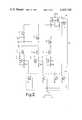
- FIG. 2shows circuit details of OSD signal translating network 64, and OSD DISABLE network 58.
- Signals G R , G G and G B from character generator 62each correspond to a tri-state logic signal.
- Translating network 64includes a tri-state logic circuit which: in a first logic state exhibits a high impedance and produces a level of +1.6 volts when no character information is to be displayed (i.e., when the kinescope is intended to respond normally to display broadcast video signals); in a second logic state exhibits a low impedance and produces a level of less than +0.8 volts when character information is to be displayed with a color other than black; and in a third logic state exhibits a low impedance and produces a level of greater than +2.4 volts when black character information is to be displayed.
- Circuit 64comprises complementary conductivity type emitter coupled, emitter input transistor pairs 80 and 81, 82 and 83, and 84 and 85 which respectively respond to character signals G R , G G and G B .
- Collector currents conducted by transistors 81, 83 and 85are respectively replicated by means of current mirror circuits including transistor 90 and diode 91, transistor 92 and diode 93, and transistor 94 and diode 95.
- Character switching control signals R, G and Bare derived from the collector outputs of transistors 90, 92 and 94.
- the levels of signals R, G and Bare a function of the conductive state of associated current mirror transistors 90, 92 and 94 in response to the level of character signals G R , G G and G B .
- Collector currents conducted by transistors 80, 82 and 84are combined and replicated by means of current mirror circuits including diode connected transistor 100 and transistor 101, and diode 104 and transistor 108.
- Character switching control signal Wis derived from the collector output of transistor 108.
- the level of signal Wis a function of the conductive state of current mirror transistor 108 in response to the character signals from generator 62.
- Translating circuit 64is discussed in greater detail in a copending U.S. patent application Ser. No. 323,351 of R. L. Shanley, II, et al. titled "Translating Circuit for Television Receiver On-Screen Graphics Display Signals.”
- Network 58comprises transistors 110, 112, 114 and 116 which respond to positive pulse V K and have collector outputs respectively coupled to "black drive” output transistors 90, 92, 94 and to "white drive” output transistor 108.
- transistors 110, 112, 114 and 116are rendered conductive and serve to maintain R, G, B and W output drive transistors 90, 92, 94 and 108 in a substantially non-conductive state corresponding to a condition wherein normal video signal information would be displayed by the kinescope. As noted earlier, however, normal video signal information is blanked during the AKB intervals.
- character signal drive transistorsare rendered inoperative to produce black and white drive character signals in response to unwanted signals including spurious signals likely to be picked up by the often lengthy conductors coupling the OSD system to color processor 20a, whereby the OSD system is disabled and prevented from producing false character representative signals.
- FIG. 3shows circuit details of signal coupling network 32 and OSD switch 66 shown in FIG. 1.
- Signal coupling network 32comprises cascade connected emitter follower transistors 120, 122 and 124 connected between the output of matrix amplifier 30 and the input of kinescope driver 34.
- the "white drive" character control signal Wis coupled to the emitter of transistor 120 in network 32 via a differential amplifier 130 and darlington-connected emitter follower transistors 132 and 134.
- Character control signal Ris applied to OSD switch 66 which comprises differentially connected current steering switching transistors 136, 138.
- signal coupling transistors 120, 122 and 124are rendered conductive in response to signals R and W in a normal video display operating mode of the receiver. At this time transistors 132, 134 are rendered non-conductive in response to signal W. Signal R renders transistor 136 conductive and transistor 138 non-conductive. At this time color signal processors 20b and 20c exhibit the same operating condition as color processor 20a.
- control signals R and Wrender video signal coupling transistor 120 non-conductive, whereby the output of matrix amplifier 30 is decoupled from the input of kinescope driver 34.
- Transistors 132 and 134remain conductive whenever a character of a color other than black is to be displayed.
- a black characteris produced whenever transistor 138, and the corresponding transistors in processors 20b and 20c, are rendered respectively conductive in response to signals R, G and B, at which time the outputs of the signal coupling networks, and thereby the outputs of color processors 20a, 20b and 20c, are blanked.
- Characters with colors white, red, green, blue, yellow, cyan and magentacan be displayed by unblanking the outputs of appropriate combinations of color processors 20a, 20b and 20c in response to control signals R, G and B.
- transistors 132, 134are rendered non-conductive in response to signal W, and switching transistors 136 and 138 are respectively rendered conductive and non-conductive in response to signal R, whereby signal coupling transistors 120, 122 and 124 are rendered conductive as in the normal video display mode.
- color signal processing networks 20b and 20cexhibit the same operating condition as network 20a.
- disabling the OSD systemcan be advantageous when accomplished at times other than during AKB intervals, such as during times when the black reference level of the video signal is sensed to develop a control voltage for controlling the DC level of the video signal, for example.
- the receivermay include a keyed comparator and clamp arrangement for developing a control voltage representative of the difference between a reference voltage and the video signal black reference level associated with each horizontal blanking interval of the video signal.
- a convenient and desirable point for sensing the video signal black levelis just prior to the kinescope driver stage (e.g., at the emitter of signal coupling transistor 120 shown in FIG. 3).
- a clamping comparator arrangement of this typeis shown in U.S. Pat. No. 4,143,398 of L. A. Harwood, et al. In this instance disabling the OSD system during the black reference level intervals will present false character signals from distorting the video signal black reference level being sensed.
Landscapes
- Engineering & Computer Science (AREA)
- Multimedia (AREA)
- Signal Processing (AREA)
- Processing Of Color Television Signals (AREA)
- Studio Circuits (AREA)
- Picture Signal Circuits (AREA)
- Television Systems (AREA)
- Controls And Circuits For Display Device (AREA)
Abstract
Description
Claims (5)
Priority Applications (15)
| Application Number | Priority Date | Filing Date | Title |
|---|---|---|---|
| US06/352,884US4435729A (en) | 1982-02-26 | 1982-02-26 | Television receiver with selectively disabled on-screen character display system |
| CA000420165ACA1192991A (en) | 1982-02-26 | 1983-01-25 | Television receiver with selectively disabled on- screen character display system |
| IT19446/83AIT1171054B (en) | 1982-02-26 | 1983-02-04 | TELEVISION RECEIVER EQUIPPED WITH A SYSTEM, SELECTIVELY DEACTIVATED, FOR THE DISPLAY OF CHARACTERS ON THE SCREEN |
| GB08303807AGB2116008B (en) | 1982-02-26 | 1983-02-11 | Video system with selectively disabled on-screen character display system |
| FI830561AFI73110C (en) | 1982-02-26 | 1983-02-18 | Television receivers with a selectively useful system for displaying characters on the frame. |
| SE8300911ASE453245B (en) | 1982-02-26 | 1983-02-18 | TELEVISION RECEIVER WITH SELECTIVE DISCONNECTABLE SYSTEM FOR PRESENTING THE SCREEN ON THE SCREEN |
| ES519900AES519900A0 (en) | 1982-02-26 | 1983-02-18 | IMPROVEMENTS INTRODUCED IN A DEVICE USED IN A SYSTEM TO TREAT VIDEO REPRESENTATIVE IMAGE SIGNALS. |
| JP58030203AJPH0744667B2 (en) | 1982-02-26 | 1983-02-24 | Video signal processing method |
| DE3306518ADE3306518C2 (en) | 1982-02-26 | 1983-02-24 | Arrangement for processing video signals containing image information |
| FR8303161AFR2522455B1 (en) | 1982-02-26 | 1983-02-25 | TELEVISION WITH SYSTEM FOR VIEWING CHARACTERS ON THE SELECTIVE INHIBITION SCREEN |
| DK091783ADK163163C (en) | 1982-02-26 | 1983-02-25 | TELEVISION RECEIVER INCLUDING ON THE SCREEN SCREEN A SIGNAL REPLACEMENT SELECTIVE |
| KR1019830000771AKR910009560B1 (en) | 1982-02-26 | 1983-02-25 | Television receiver with selectively disable on-screen character display system |
| AT0069683AAT386712B (en) | 1982-02-26 | 1983-02-28 | TELEVISION PLAYER WITH A CHARACTERISTIC SIGNALING DEVICE |
| HK180/87AHK18087A (en) | 1982-02-26 | 1987-02-26 | Video system with selectively disabled on-screen character display system |
| MY393/87AMY8700393A (en) | 1982-02-26 | 1987-12-30 | Video system with selective disable on-screen character display |
Applications Claiming Priority (1)
| Application Number | Priority Date | Filing Date | Title |
|---|---|---|---|
| US06/352,884US4435729A (en) | 1982-02-26 | 1982-02-26 | Television receiver with selectively disabled on-screen character display system |
Publications (1)
| Publication Number | Publication Date |
|---|---|
| US4435729Atrue US4435729A (en) | 1984-03-06 |
Family
ID=23386895
Family Applications (1)
| Application Number | Title | Priority Date | Filing Date |
|---|---|---|---|
| US06/352,884Expired - LifetimeUS4435729A (en) | 1982-02-26 | 1982-02-26 | Television receiver with selectively disabled on-screen character display system |
Country Status (15)
| Country | Link |
|---|---|
| US (1) | US4435729A (en) |
| JP (1) | JPH0744667B2 (en) |
| KR (1) | KR910009560B1 (en) |
| AT (1) | AT386712B (en) |
| CA (1) | CA1192991A (en) |
| DE (1) | DE3306518C2 (en) |
| DK (1) | DK163163C (en) |
| ES (1) | ES519900A0 (en) |
| FI (1) | FI73110C (en) |
| FR (1) | FR2522455B1 (en) |
| GB (1) | GB2116008B (en) |
| HK (1) | HK18087A (en) |
| IT (1) | IT1171054B (en) |
| MY (1) | MY8700393A (en) |
| SE (1) | SE453245B (en) |
Cited By (7)
| Publication number | Priority date | Publication date | Assignee | Title |
|---|---|---|---|---|
| US4622589A (en)* | 1985-04-15 | 1986-11-11 | Rca Corporation | Television receiver on-screen character display |
| US4748506A (en)* | 1984-12-28 | 1988-05-31 | Canon Kabushiki Kaisha | Image pickup apparatus with excess-charge control |
| US4849818A (en)* | 1985-05-17 | 1989-07-18 | Deutsche Thomson-Brandt Gmbh | Television receiver with receiving devices for processing videotext and teletext signals |
| US5027211A (en)* | 1989-06-07 | 1991-06-25 | Robertson Bruce W | Multi-channel message display system and method |
| US5386238A (en)* | 1992-01-09 | 1995-01-31 | U.S. Philips Corporation | Combination TV receiver and teletext processor with on-screen message capability |
| US20030103143A1 (en)* | 2001-12-05 | 2003-06-05 | Shin Fujimori | Cutoff control with on screen display circuit for adjusting white balance |
| US20070236607A1 (en)* | 2004-08-10 | 2007-10-11 | Morris Robert E | Method and Apparatus for Controlling a Display Function |
Families Citing this family (2)
| Publication number | Priority date | Publication date | Assignee | Title |
|---|---|---|---|---|
| US4689663A (en)* | 1985-09-27 | 1987-08-25 | Rca Corporation | Television receiver with display driver amplifier and input video filter having inversely related bandwidths |
| DE3905925A1 (en)* | 1989-02-25 | 1990-08-30 | Thomson Brandt Gmbh | METHOD FOR RECORDING AND / OR IMAGING A TELEVISION SUBSCRIPTION |
Citations (6)
| Publication number | Priority date | Publication date | Assignee | Title |
|---|---|---|---|---|
| US3891792A (en) | 1974-06-25 | 1975-06-24 | Asahi Broadcasting | Television character crawl display method and apparatus |
| US3898644A (en) | 1973-09-13 | 1975-08-05 | Qsi Systems Inc | TV display system |
| US3911420A (en) | 1973-11-23 | 1975-10-07 | Xerox Corp | Display system including a high resolution character generator |
| US3984828A (en) | 1975-05-23 | 1976-10-05 | Rca Corporation | Character generator for television channel number display with edging provisions |
| US4021841A (en) | 1975-12-31 | 1977-05-03 | Ralph Weinger | Color video synthesizer with improved image control means |
| US4345246A (en) | 1979-06-20 | 1982-08-17 | Thomson-Csf | Synchronization device for a character-generating circuit and a vertical scanning circuit and television receiver comprising such a device |
Family Cites Families (3)
| Publication number | Priority date | Publication date | Assignee | Title |
|---|---|---|---|---|
| DE2649445C2 (en)* | 1976-10-29 | 1982-09-09 | Deutsche Itt Industries Gmbh, 7800 Freiburg | Television receiver with a built-in timer |
| US4218698A (en)* | 1978-03-13 | 1980-08-19 | Rca Corporation | TV Graphics and mixing control |
| US4263622A (en)* | 1979-01-30 | 1981-04-21 | Rca Corporation | Automatic kinescope biasing system |
- 1982
- 1982-02-26USUS06/352,884patent/US4435729A/ennot_activeExpired - Lifetime
- 1983
- 1983-01-25CACA000420165Apatent/CA1192991A/ennot_activeExpired
- 1983-02-04ITIT19446/83Apatent/IT1171054B/enactive
- 1983-02-11GBGB08303807Apatent/GB2116008B/ennot_activeExpired
- 1983-02-18ESES519900Apatent/ES519900A0/enactiveGranted
- 1983-02-18SESE8300911Apatent/SE453245B/ennot_activeIP Right Cessation
- 1983-02-18FIFI830561Apatent/FI73110C/ennot_activeIP Right Cessation
- 1983-02-24JPJP58030203Apatent/JPH0744667B2/ennot_activeExpired - Lifetime
- 1983-02-24DEDE3306518Apatent/DE3306518C2/ennot_activeExpired
- 1983-02-25DKDK091783Apatent/DK163163C/ennot_activeIP Right Cessation
- 1983-02-25KRKR1019830000771Apatent/KR910009560B1/ennot_activeExpired
- 1983-02-25FRFR8303161Apatent/FR2522455B1/ennot_activeExpired
- 1983-02-28ATAT0069683Apatent/AT386712B/ennot_activeIP Right Cessation
- 1987
- 1987-02-26HKHK180/87Apatent/HK18087A/ennot_activeIP Right Cessation
- 1987-12-30MYMY393/87Apatent/MY8700393A/enunknown
Patent Citations (6)
| Publication number | Priority date | Publication date | Assignee | Title |
|---|---|---|---|---|
| US3898644A (en) | 1973-09-13 | 1975-08-05 | Qsi Systems Inc | TV display system |
| US3911420A (en) | 1973-11-23 | 1975-10-07 | Xerox Corp | Display system including a high resolution character generator |
| US3891792A (en) | 1974-06-25 | 1975-06-24 | Asahi Broadcasting | Television character crawl display method and apparatus |
| US3984828A (en) | 1975-05-23 | 1976-10-05 | Rca Corporation | Character generator for television channel number display with edging provisions |
| US4021841A (en) | 1975-12-31 | 1977-05-03 | Ralph Weinger | Color video synthesizer with improved image control means |
| US4345246A (en) | 1979-06-20 | 1982-08-17 | Thomson-Csf | Synchronization device for a character-generating circuit and a vertical scanning circuit and television receiver comprising such a device |
Non-Patent Citations (3)
| Title |
|---|
| "Analysis and Design of Integrated Electronic Circuits" (Chirlian) p. 133, Harper and Row, 1981. |
| "Digital Integrated Electronics" (Taub and Schilling), p. 452 McGraw Hill 1977. |
| Schematic Circuit Diagram of a Portion of the Signal Processing System of the Metz Color Television Receiver, Chassis 681 G. |
Cited By (10)
| Publication number | Priority date | Publication date | Assignee | Title |
|---|---|---|---|---|
| US4748506A (en)* | 1984-12-28 | 1988-05-31 | Canon Kabushiki Kaisha | Image pickup apparatus with excess-charge control |
| US4622589A (en)* | 1985-04-15 | 1986-11-11 | Rca Corporation | Television receiver on-screen character display |
| US4849818A (en)* | 1985-05-17 | 1989-07-18 | Deutsche Thomson-Brandt Gmbh | Television receiver with receiving devices for processing videotext and teletext signals |
| US5027211A (en)* | 1989-06-07 | 1991-06-25 | Robertson Bruce W | Multi-channel message display system and method |
| US5386238A (en)* | 1992-01-09 | 1995-01-31 | U.S. Philips Corporation | Combination TV receiver and teletext processor with on-screen message capability |
| US20030103143A1 (en)* | 2001-12-05 | 2003-06-05 | Shin Fujimori | Cutoff control with on screen display circuit for adjusting white balance |
| WO2003051037A1 (en)* | 2001-12-05 | 2003-06-19 | Sony Electronics Inc. | Cutoff control with on screen display circuit for adjusting white balance |
| US6891564B2 (en) | 2001-12-05 | 2005-05-10 | Sony Corporation | Cutoff control with on screen display circuit for adjusting white balance |
| US20070236607A1 (en)* | 2004-08-10 | 2007-10-11 | Morris Robert E | Method and Apparatus for Controlling a Display Function |
| US8228434B2 (en)* | 2004-08-10 | 2012-07-24 | Thomson Licensing | Method and apparatus for adjusting a display in an extinguished state |
Also Published As
| Publication number | Publication date |
|---|---|
| FR2522455A1 (en) | 1983-09-02 |
| HK18087A (en) | 1987-03-06 |
| CA1192991A (en) | 1985-09-03 |
| ES8403265A1 (en) | 1984-03-01 |
| FR2522455B1 (en) | 1986-04-11 |
| DK91783D0 (en) | 1983-02-25 |
| GB8303807D0 (en) | 1983-03-16 |
| DK163163B (en) | 1992-01-27 |
| KR910009560B1 (en) | 1991-11-21 |
| DK91783A (en) | 1983-08-27 |
| SE8300911L (en) | 1983-08-27 |
| IT1171054B (en) | 1987-06-10 |
| SE453245B (en) | 1988-01-18 |
| DE3306518A1 (en) | 1983-09-08 |
| FI830561A0 (en) | 1983-02-18 |
| FI73110C (en) | 1987-08-10 |
| FI830561L (en) | 1983-08-27 |
| AT386712B (en) | 1988-10-10 |
| MY8700393A (en) | 1987-12-31 |
| ATA69683A (en) | 1988-02-15 |
| JPH0744667B2 (en) | 1995-05-15 |
| KR840003948A (en) | 1984-10-04 |
| GB2116008B (en) | 1985-11-27 |
| ES519900A0 (en) | 1984-03-01 |
| DE3306518C2 (en) | 1986-03-06 |
| JPS58159077A (en) | 1983-09-21 |
| GB2116008A (en) | 1983-09-14 |
| FI73110B (en) | 1987-04-30 |
| SE8300911D0 (en) | 1983-02-18 |
| DK163163C (en) | 1992-06-22 |
| IT8319446A0 (en) | 1983-02-04 |
Similar Documents
| Publication | Publication Date | Title |
|---|---|---|
| US4412244A (en) | Switching circuit for television receiver on-screen display | |
| FI74374B (en) | FRAMEWORK FOR THE IMPLEMENTATION OF THE TELEVISION IMPLEMENTATION. | |
| US4599642A (en) | Video signal processor with bias error compensation | |
| US4516152A (en) | Video signal processor with automatic kinescope white balance and beam current limiter control systems | |
| US4253121A (en) | Plural sequential operating mode automatic kinescope beam current limiter | |
| US4435729A (en) | Television receiver with selectively disabled on-screen character display system | |
| US4354202A (en) | Television receiver on-screen alphanumeric display | |
| US4110787A (en) | Combined blanking level and kinescope bias clamp for a television signal processing system | |
| US4554578A (en) | Error compensated control system in a video signal processor | |
| US4432016A (en) | Translating circuit for television receiver on-screen graphics display signals | |
| US4584596A (en) | Television receiver alignment system | |
| US4489344A (en) | Signal processing unit | |
| US4313130A (en) | Keying signal generator with false output immunity | |
| US3647944A (en) | Kinescope bias arrangement to provide both constant amplitude dc restoration pulses and arc discharge protection | |
| EP0512332B1 (en) | A television system having an ultrablack video signal blanking level for an on-screen character display | |
| CA1219353A (en) | Video signal processor with bias error compensation | |
| EP0146343A2 (en) | Control system for luminance/chrominance signal processing circuits | |
| CA1214859A (en) | Television receiver alignment system | |
| JPH06311446A (en) | Closed caption decoder system and circuit |
Legal Events
| Date | Code | Title | Description |
|---|---|---|---|
| AS | Assignment | Owner name:RCA CORPORATION, A CORP OF DE Free format text:ASSIGNMENT OF ASSIGNORS INTEREST.;ASSIGNORS:HARWOOD, LEOPOLD A.;SHANLEY, ROBERT L. II;REEL/FRAME:003993/0763 Effective date:19820224 Owner name:RCA CORPORATION, A CORP OF DE,NEW JERSEY Free format text:ASSIGNMENT OF ASSIGNORS INTEREST;ASSIGNORS:HARWOOD, LEOPOLD A.;SHANLEY, ROBERT L. II;REEL/FRAME:003993/0763 Effective date:19820224 | |
| STCF | Information on status: patent grant | Free format text:PATENTED CASE | |
| MAFP | Maintenance fee payment | Free format text:PAYMENT OF MAINTENANCE FEE, 4TH YEAR, PL 96-517 (ORIGINAL EVENT CODE: M170); ENTITY STATUS OF PATENT OWNER: LARGE ENTITY Year of fee payment:4 | |
| AS | Assignment | Owner name:RCA LICENSING CORPORATION, TWO INDEPENDENCE WAY, PRINCETON, NJ 08540, A CORP. OF DE Free format text:ASSIGNMENT OF ASSIGNORS INTEREST;ASSIGNOR:RCA CORPORATION, A CORP. OF DE;REEL/FRAME:004993/0131 Effective date:19871208 Owner name:RCA LICENSING CORPORATION, TWO INDEPENDENCE WAY, P Free format text:ASSIGNMENT OF ASSIGNORS INTEREST.;ASSIGNOR:RCA CORPORATION, A CORP. OF DE;REEL/FRAME:004993/0131 Effective date:19871208 | |
| MAFP | Maintenance fee payment | Free format text:PAYMENT OF MAINTENANCE FEE, 8TH YEAR, PL 96-517 (ORIGINAL EVENT CODE: M171); ENTITY STATUS OF PATENT OWNER: LARGE ENTITY Year of fee payment:8 | |
| MAFP | Maintenance fee payment | Free format text:PAYMENT OF MAINTENANCE FEE, 12TH YEAR, LARGE ENTITY (ORIGINAL EVENT CODE: M185); ENTITY STATUS OF PATENT OWNER: LARGE ENTITY Year of fee payment:12 | |
| FEPP | Fee payment procedure | Free format text:PAYOR NUMBER ASSIGNED (ORIGINAL EVENT CODE: ASPN); ENTITY STATUS OF PATENT OWNER: LARGE ENTITY |