US4434322A - Coded data transmission system - Google Patents
Coded data transmission systemDownload PDFInfo
- Publication number
- US4434322A US4434322AUS06/286,356US28635681AUS4434322AUS 4434322 AUS4434322 AUS 4434322AUS 28635681 AUS28635681 AUS 28635681AUS 4434322 AUS4434322 AUS 4434322A
- Authority
- US
- United States
- Prior art keywords
- signal
- shift register
- output
- data
- information
- Prior art date
- Legal status (The legal status is an assumption and is not a legal conclusion. Google has not performed a legal analysis and makes no representation as to the accuracy of the status listed.)
- Expired - Lifetime
Links
- 230000005540biological transmissionEffects0.000titleclaimsabstractdescription56
- 238000000034methodMethods0.000claimsdescription7
- 238000001514detection methodMethods0.000claimsdescription5
- 238000000605extractionMethods0.000claimsdescription2
- 238000013500data storageMethods0.000claims11
- 230000008878couplingEffects0.000claims7
- 238000010168coupling processMethods0.000claims7
- 238000005859coupling reactionMethods0.000claims7
- 230000001131transforming effectEffects0.000claims3
- 238000009877renderingMethods0.000abstract1
- 238000010586diagramMethods0.000description6
- 230000004075alterationEffects0.000description2
- 230000000737periodic effectEffects0.000description2
- 230000001755vocal effectEffects0.000description2
- 229910002056binary alloyInorganic materials0.000description1
- 239000013078crystalSubstances0.000description1
- 230000001351cycling effectEffects0.000description1
- 238000006073displacement reactionMethods0.000description1
- 230000007257malfunctionEffects0.000description1
- 238000012986modificationMethods0.000description1
- 230000004048modificationEffects0.000description1
- 230000000007visual effectEffects0.000description1
Images

Classifications
- H—ELECTRICITY
- H04—ELECTRIC COMMUNICATION TECHNIQUE
- H04K—SECRET COMMUNICATION; JAMMING OF COMMUNICATION
- H04K1/00—Secret communication
- H04K1/02—Secret communication by adding a second signal to make the desired signal unintelligible
Definitions
- the present inventionrelates generally to the transmission of information between two separated points and more particularly to a coded data transmission system including a novel transmitter and novel receiver which make possible the transmission of data between two points in a manner such that jamming attempts may be readily recognized by short term intermittent checking and also such that the possibility of an intruder being able to decode the stream of information is rendered remote.
- Another object of the present inventionis to provide a recording system including protection means for making it possible to detect any alterations or attempted alterations in the recorded information.
- Another object of the present inventionis to provide an improved coded information transmission system using high speed shift registers in the transmitter and in the receiver and wherein real time coincidence between the shifting of information in the transmitter and receiver is not required.
- a further object of the present inventionis to provide a simplified system for checking the proper operation of a high speed multi-stage shift register.
- the output signals from a multi-stage binary shift registerare applied to an arbitrary logic network in a manner such that any preselected combinations of conditions of the individual stages in the shift register will cause the arbitrary logic network to provide one or the other of two output signals.
- the output signal from the arbitrary logic networkis applied to a binary half-adder or a unit which is commonly referred to in the art as a modulo-two-adder.
- a modulo-two-adderhas the characteristic that when each of its two input circuits are simultaneously provided with "ones" or “zeros" the output circuit thereof is provided with a "zero" output.
- the output circuitis provided with a "one" output.
- the terms "one” and “zero”are meant to refer to the common terminology used in the binary art wherein two distinct signal levels are characterized as respectively representing a “one” or a “zero” in binary notation.
- the second input circuit for the first modulo-two-adderis adpated to receive binary input data signals while the output circuit of the modulo-two-adder is connected to any suitable signal transmitter and is also connected to the input circuit of the first bistable storage unit in the shift register.
- a suitable clock pulse generatorserves to provide timing signals in a conventional manner to the various stages in the shift register so that the shifting of information along the chain of bistable units will occur at a regular and controlled rate.
- the receiver unitincludes components substantially identical to those described for the transmitter but the manner in which the various components are connected differs substantially from the manner of connection of the components in the transmitter. That is, the receiver includes a multi-stage shift register having the same number of stages as does the shift register in the transmitter. The receiver similarly contains an arbitrary logic network which is identical to the arbitrary logic network in the transmitter. A second modulo-two-adder has a first input circuit connected to the output circuit of the arbitrary logic network in the receiver, and a second input circuit to which the signals from the transmitter are applied. The transmitted signals are simultaneously applied to the first stage of the multi-stage shift register of the receiver unit.
- a second clock pulse generatoradapted to provide periodic control signals at the same repetition rate as does the first clock pulse generator in the transmitter, is coupled with each of the bistable elements of the shift register in the receiver.
- the transmitter and receivereach contain substantially identical shift registers, arbitrary logic networks, and clock pulse generators, as well as each including a modulo-two-adder.
- the circuit arrangement for the transmitteris such that the shift register can be referred to as a feed-back shift register in that the output signals from the shift register are passed through an arbitrary logic network, through a modulo-two-adder, and back to the input circuit for the shift register.
- the shift register in the receivercan be referred to as a feed-forward shift register, since the only signals applied to the input thereof are the output signals transmitted by the transmitter, with the output signals from the shift register in the receiver being passed through the arbitrary logic network and the modulo-two-adder where they are added directly in mod-two fashion to the input signals received by the receiver.
- the result of the combination of the above generally described transmitter and receiveris such that the state of the shift register in the receiver will become coincident with the state of the shift register in the transmitter after a period of time equal to n clock pulse time intervals. Then thereafter with the two arbitrary logic networks being set to identical modes, the shift registers in the transmitter and the receiver will remain in identical conditions.
- the transmitteris made to transmit a series of "zeros" either intermittently or continuously between message transfer times, the receiver output can be observed to see if jamming or "spoofing" is being attempted.
- the output of the receiver unitwill be zero unless an erroneous signal is received during the time when the input information circuit for the transmitter applies a continuing zero signal to the main modulo-two-adder in the transmitter. If an attempt is made to cause the transmission of erroneous information by jamming techniques, such attempt would be readily detected at the receiver by a presence of a "one" in the receiver output circuit.
- the transmission of datacan take place by the application of clocked binary information to the input circuit of the transmitter.
- the contents of the shift register in the transmitterwill, of course, be changed and will undergo such change at a known rate as a result of the cycling of the clock pulse generator.
- the output circuit of the shift register and the arbitrary logic network in the transmitterwill cause a changing code signal to be applied to one input of the modulo-two-adder.
- the information to be transmittedwill then be added modulo-two to a changing code and thus the output of the modulo-two-adder will bear no resemblance to the information to be transmitted.
- the output of the mod-two adderis used to control the output of a conventional r-f transmitter. Accordingly, the signal information stream being transmitted by the r-f transmitter will bear no particular resemblance to the actual information being transmitted.
- the output signal from the arbitrary logic network of the transmitteris effectively removed from the code stream by a modulo-two-addition so that the result is an output code signal stream from the receiver which is identical to the code stream originally applied to the input circuit of the transmitter.
- the systemalso makes possible the accurate and rapid checking of the operation of a multi-stage shift register operating at a high speed.
- the only thing required for checking the accurate operation of the high speed shift register in the transmitteris to have one input circuit for the modulo-two-adder associated with the shift register being checked (in the "transmitter") maintained at one or the other of a one or a zero condition.
- the output circuit of the "receiver”will then continuously provide a one or a zero output if both shift registers are operating properly.
- the transmitter described aboveis used to apply a background signal to a recording apparatus which is being used to record any desired information, as for example verbal information.
- any desired informationas for example verbal information.
- any attempt to modify the recordingwould result in the loss or displacement of at least one binary bit and, of course, the loss of even one bit would result in the output signal from the receiver having other than a signal corresponding to the code signal applied as an input to the mod-two adder during recording.
- the mod-two adder in the "transmitter"is provided with all zeros during recording. The output of the receiver is then merely observed for the presence of a one as an indication of an attempt to alter the record.
- FIG. 1Ais a block diagram of an improved coded information transmitter provided in accordance with the teachings of the present invention.
- FIG. 1Bis a block diagram of a coded information receiver making use of parts substantially identical to those of the transmitter in FIG. 1A, but with the various components being connected in a different circuit arrangement.
- FIG. 2is a more detailed block diagram of a four-stage binary feed-back shift register and modulo-two-adder in combination with one example of a simplified arbitrary logic network which may be used in the systems of FIGS. 1A and 1B.
- FIG. 3Ais a block diagram of a tamper-proof recording system making use of the teachings of the present invention.
- FIG. 3Bis a block diagram of a record playback system adapted for use with the recording system of FIG. 3A.
- FIG. 3Cis a block diagram of a system similar to that of FIG. 3B but including apparatus for using a changing code input on the recorder and on the playback to further prevent undetectable tampering with the record.
- FIG. 4is a system for checking the operation of high speed multi-stage shift registers.
- the systemincludes a multi-stage shift register 10 which for purpose of illustration and explanation of the present invention will be referred to as a multi-stage bistable feed-back shift register 10 having individual bistable stages 1, 2, 3, 4, 5,-n where n can be any integer.
- Each of the binary stages 1-nmay be a conventional flip-flop provided with a signal output circuit 101, 102, 103, 104, 105, 10n, which is connected as an input circuit for an arbitrary logic network 12.
- the arbitrary logic network 12has a signal output circuit 13 which is connected to one of the input circuits for a modulo-two-adder 14 having a signal or data input circuit 15A connected thereto for the receipt of information to be transmitted.
- an input signal source 15is shown connected to input circuit 15A.
- the transmitter shown in FIG. 1Awill be referred to for purpose of teaching the invention as operating in the binary system and therefore the input circuit 15A is provided with binary signals referred to as "zero" or "one” signals, as is common in the art.
- Such informationcould be the conventional teletype code or could be digitized speech which is well known and widely used at the present time.
- the modulo-two-addermay also be referred to as a binary half-adder in that if each of its input circuits simultaneously receive a one, or simultaneously receive a zero, the output circuit 16 thereof will have a zero signal level. If either of the two input circuits for the modulo-two-adder 14 is at a one level, but the other is at a zero level, the output circuit 16 will be at a one level. It will be seen that the output circuit 16 is directly connected to a suitable r-f transmitter network 17 which can be any of a number known in the art.
- the transmitter 17can be a pulsed radio frequency transmitter adapted to be operated in an on-off mode or adapted to be continuously operated but made to operate at one or the other of two frequencies, one or the other of two phases, or any other suitable arrangement wherein two distinct types of signals are transmitted in accordance with the signal level of the output circuit 16 for the modulo-two-adder 14.
- a branch circuit 18will be seen to be connected from the output circuit 16 of the modulo-two-adder 14 directly to the first stage of the shift register 10.
- a suitable clock pulse generator 19will be seen to have a signal output circuit 20 which is connected to each of the binary stages of the multi-stage shift register 10 in a manner such that the clock pulse generator will serve to cause the advance of information down the shift register at a regular and controlled recurring rate.
- the receiver shown in FIG. 1Bis adapted to cooperate with the transmitter of FIG. 1A to provide a complete data transmission system and will be seen to include components which are substantially identical to the components of the transmitter.
- the receiverincludes a second binary shift register 40 (referred to as a feed-forward shift register) having a number of stages n which number is identical to the number of stages in the first binary shift register 10 of the transmitter.
- Each of the individual bistable stages of the second shift register 40will be seen to have a signal output circuit 401, 402, 403, 404, 405, 40n with each of said output circuits of the bistable stages being connected as an input to the arbitrary logic network 42.
- Arbitrary logic network 42is identical to the arbitrary logic network 12 in the transmitter.
- the arbitrary logic network 42has a signal output circuit 43 which is connected as a first input to a second modulo-two-adder 44.
- a decoded signal output circuit 45will be seen to be provided as the output circuit from the second modulo-two-adder 44.
- the second signal input circuit 46 for the second modulo-two-adder 44is directly connected to the output circuit of the information receiving network 47.
- the receiver 47is a conventional radio frequency receiver adpated to cooperate with and detect the signals from the r-f transmitter 17 and provide on its output circuit 48 binary signals corresponding to those applied to the r-f transmitter 17.
- the signal output circuit 48 for the receiver 47is also connected to the input circuit 49 for the first or lowest order stage of the multi-stage shift register 40.
- a second clock pulse generator 50which operates to provide recurring pulses at time intervals the same as the time intervals between the clock pulses of the first clock pulse generator 19 has a signal output circuit 51 directly connected to each of the stages of the second binary shift register 40.
- the r-f receiver 47will receive the signal information transmitted by the r-f transmitter 17, and apply on its output circuit 48 binary coded signals corresponding to the binary coded output signals from the modulo-two adder 14 in the transmitter. Since the arbitrary logic network 42 is established as being identical to the arbitrary logic network 12, and since the feed-forward shift register 40 was initially in the same condition as was the feed-back shift register 10 it will be seen that the shift registers 10 and 40 receive identical inputs and thus the output signals from the arbitrary logic network 42 applied to the second modulo-two adder 44 will be identical to the signals applied from the arbitrary logic network 12 to the first modulo-two adder 14.
- the transmitted signal trainwill be seen to be applied over the circuit 46 as the second input for the second modulo-two adder 44.
- the resultis that the output of mod-two adder 14 is added mod-two to the signal from logic network 12, which of course is itself the signal added mod-two to the input data from source 15.
- the same signalis effectively added twice in modulo-two fashion to the original signal applied from the input signal source over circuit 15A to the first modulo-two adder 14.
- the resultis that the original input signal will be provided on the signal output circuit 45 from the modulo-two adder 44 as the output signals 60'.
- Thiscan be shown by the following set of logical equations wherein the plus sign (+) represents an addition being performed in modulo-two fashion. It should be mentioned that modulo-two addition is also frequently described in the art as applying signals to an "exclusive-or" gate.
- the input signal applied to the transmission networkwill be transmitted in a coded fashion which bears no particular relationship to the applied signal information and yet the output signals from the modulo-two adder 44 will always correspond to the input signals applied to the modulo-two adder 14.
- the transmitter and the receivercan be time-displaced and need not be in real-time coincidence. That is, it is only necessary that the clock pulse generator 50 provide output signals at the same repetition rate as the clock pulse generator 19. It is not necessary that the output signals from the two clock pulse generators take place at the same real instant in time. With the present state of the clock pulse generation art, using local crystal oscillators, or digital timing extractors, these objectives are readily achieved and yet the necessity for a real time control link between the transmitter and the receiver is not required.
- the systemhas the inherent capability to make possible an easy check to ascertain whether or not a third party is attempting to jam or garble the signal information. That is, it will be seen that the output signals 60' are identical to the input signals 60. Thus if the input signal source 15 provides a continuing series of zero signals, then the output from the mod-two adder 44 in the receiver will be zero only so long as no erroneous information is being received. The receipt of a single one in the output of the mod-two adder 44 would be an indication that a third party was attempting to jam the system.
- the present inventionmakes possible the checking of a high speed shift register such as the feed-back and feed-forward shift registers 10 and 40 merely by maintaining the signal on the signal input circuit 15A at a zero level and observing the output signal from the modulo-two adder 44 in the receiver. That is, the output circuit of the modulo-two adder 44 under such conditions will remain at a zero level only so long as the feed-back shift register 10 is operating properly.
- This method and apparatus for checking the proper operation of the feed-back shift register 10is illustrated in FIG. 4 wherein it will be seen that the output signal from the arbitrary logic network 114 is connected directly as an input circuit for the second modulo-two adder 144 and as an input for the first stage for the feed-forward shift register 140.
- a "one" detector 141is connected to the mod-two adder 144, and may for example be a bistable circuit which is changed from one condition to another upon receipt of a one from the mod-two adder 144.
- An indicator 143 driven by the detector 141provides a visual indication of malfunction of one of the shift registers.
- FIG. 3Athere is shown an improved recording system making use of the teachings of the present invention to provide a record which is essentially tamper proof in that any attempt to alter the information recorded by the system will be immediately detected when the record thus made is later played back.
- the system of FIG. 3Aincludes a transmitter substantially the same as that shown in FIG. 1A in combination with a conventional recorder 200 which may for example be a magnetic tape recorder.
- a source of information to be recorded 218will be seen to be connected as one of the signal input devices for the recorder 200. In one specific application of the system verbal information serves as source 218.
- the systemincludes a feed-back shift register 210 having the signal output circuits of the individual stages thereof connected to an arbitrary logic network 212 which in turn has its output circuit 213 connected as an input for the mod-two-adder 214.
- the output signals from the modulo-two-adder 214are applied to the lowest order stage of the shift register 210 and also to the signal output device 217 which is adapted to provide output signals directly to the recorder 200.
- the output device 217can be operated at a high frequency to avoid interference with signals from source 218, the output from device 217 being in binary form.
- the code signal source 215maintains one input to the mod-two-adder 214 at zero. Therefore the output of the logic network 212 is effectively fed directly (unaltered) to the output device 217.
- FIG. 3Bthere is illustrated a play-back device 250 which is adapted to play back the record made by the recorder 200.
- the output device 260is a conventional audio speaker.
- the output signal from the record playback apparatus 250is applied to the input and demodulation device 247 which has its signal output circuit directly connected to the input circuit for the feed-forward shift register 240.
- the demodulated output signal from the demodulating input device 247is simultaneously applied to a mod-two adder 244 which has as its second input circuit the output circuit from the arbitrary logic network 242.
- the arbitrary logic network 242which is identical to the arbitrary logic network 212 is connected to each of the stages of the feed-forward shift register 240 in the manner described with reference to FIG. 1B.
- the system of FIG. 3Acan advantageously have the clock pulse generator 219 coupled with the recorder 200 (as shown by the dashed line in FIG. 3A) so that clock pulse signals are simultaneously recorded.
- a clock pulse detector 248is coupled to the demodulator 247 so that the previously recorded clock pulse signals will be detected by the clock pulse detector 248 and serve to control the shifting of information in the feed-forward shift register 240.
- the clock pulse detector 248can also include a clock pulse extractor operating on the basis of digital timing extraction so that there is no need to record clock pulse signals. and yet variations in speed of the recording medium are avoided since the clock pulse signals for the playback are derived from the recorded information itself.
- the output signal from the mod-two adder 244will remain at zero so long as the recorded check signals being demodulated and applied to the feed-forward shift register 240 are identical to those which were actually recorded during the making of the record. If any variance occurs the output from the mod-two adder 244 will change to a value other than zero and hence indicate that there has been attempt to modify the record previously made. As previously explained the two shift registers come into coincidence after n clock pulse time intervals. Thus in practice a short leader is recorded to assure coincidence of the two when playback of the desired information is initiated.
- FIG. 3Cthere is shown a more sophisticated record play-back apparatus which in addition to the components shown in FIG. 3B includes a noncoincidence detector 270 together with a code signal source 275.
- the recorder of FIG. 3Ahas its code signal source 215 made identical to the code signal source 275.
- the codes provided at the output of the code source 215will be provided at the output of the mod-two adder 244 (FIG. 3C) during playback.
- the code source 275also provides the same signals to the noncoincidence detector 270.
- the indicator 271will indicate any noncoincidence of the signals applied to detector 270 and thereby serve as a detection of any record tampering.
- the code signal sources 215 and 275are preferably recorders having recorded code patterns with the signals therefrom being controlled in time by the clock pulse generator 219 and clock pulse detector 268, respectively.
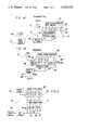
- FIG. 2a specific embodiment of a simplified logic network which includes a plurality of "AND" gates connected between the shift register and half-adder of a transmitter similar to that of FIG. 1A.
- the four-stage shift register 70is coupled through the AND gates 71 and selectively settable switches 72-77 to one of the input circuits for the half-adder 78.
- a signal source 79serves as the signal source for the other input circuit of the half-adder 78.
- the output circuit 80is directly connected to the coded output device 81 and is also connected to the input of the lowest order stage of the shift register 70.
- a clock pulse generator 82is shown as controlling the shifting of information in the shift register 70 and would also control the timing of the application of signals from the signal source 79 to the half-adder 78.
- the switch 72is closed while the remaining switches 73-77 are opened.
- the half-adder 78will have a "one” on one of its inputs whenever the first bistable unit in the shift register 70 is in a "one” condition. At all other times the half-adder would receive a zero input from the shift register 70.
- a different one of the switchescould of course be closed, the purpose of such an arrangement being to provide a system wherein the signal applied to the half-adder 78 will be controlled by the condition of the shift register 70 as modified by the arbitrary logic network.
- the arbitrary logic network associated with the receiverwould be identical to the arbitrary logic network associated with the transmitter.
Landscapes
- Engineering & Computer Science (AREA)
- Computer Networks & Wireless Communication (AREA)
- Signal Processing (AREA)
- Synchronisation In Digital Transmission Systems (AREA)
- Error Detection And Correction (AREA)
Abstract
Description
______________________________________ Input Signal to 14 Output Transmitted, Output From From Received, From Output Source Logic and Applied Logic From 15 13 To 44 42 44 ______________________________________ 1 + 1 = 0 + 1 = 1 1 + 0 = 1 + 0 = 1 0 + 1 = 1 + 1 = 0 0 + 0 = 0 + 0 = 0 ______________________________________
Claims (40)
Priority Applications (2)
| Application Number | Priority Date | Filing Date | Title |
|---|---|---|---|
| US06/286,356US4434322A (en) | 1965-08-19 | 1981-07-23 | Coded data transmission system |
| US06/557,915US4760598A (en) | 1981-07-23 | 1983-12-05 | Coded data transmission system |
Applications Claiming Priority (2)
| Application Number | Priority Date | Filing Date | Title |
|---|---|---|---|
| US48102165A | 1965-08-19 | 1965-08-19 | |
| US06/286,356US4434322A (en) | 1965-08-19 | 1981-07-23 | Coded data transmission system |
Related Parent Applications (1)
| Application Number | Title | Priority Date | Filing Date |
|---|---|---|---|
| US48102165AContinuation | 1965-08-19 | 1965-08-19 |
Related Child Applications (1)
| Application Number | Title | Priority Date | Filing Date |
|---|---|---|---|
| US06/557,915ContinuationUS4760598A (en) | 1981-07-23 | 1983-12-05 | Coded data transmission system |
Publications (1)
| Publication Number | Publication Date |
|---|---|
| US4434322Atrue US4434322A (en) | 1984-02-28 |
Family
ID=26963752
Family Applications (1)
| Application Number | Title | Priority Date | Filing Date |
|---|---|---|---|
| US06/286,356Expired - LifetimeUS4434322A (en) | 1965-08-19 | 1981-07-23 | Coded data transmission system |
Country Status (1)
| Country | Link |
|---|---|
| US (1) | US4434322A (en) |
Cited By (52)
| Publication number | Priority date | Publication date | Assignee | Title |
|---|---|---|---|---|
| US4488001A (en)* | 1981-12-17 | 1984-12-11 | Ncr Corporation | Intellectual properties protection device |
| WO1985004299A1 (en)* | 1984-03-14 | 1985-09-26 | Computer Security Systems, Inc. | Method and apparatus for protecting stored and transmitted data from compromise or interception |
| US4642424A (en)* | 1984-01-03 | 1987-02-10 | At&T Information Systems Inc. | Cryptographic transmission system |
| US4663500A (en)* | 1982-02-22 | 1987-05-05 | Nec Corporation | Cryptographic system |
| US4669118A (en)* | 1984-02-02 | 1987-05-26 | Siemens Aktiengesellschaft | Self-synchronizing descrambler |
| US4736424A (en)* | 1986-09-22 | 1988-04-05 | Rockwell International Corporation | Data scrambling apparatus |
| US4757535A (en)* | 1985-05-23 | 1988-07-12 | Alcatel N.V. | System for encrypted information transmission |
| US4771458A (en)* | 1987-03-12 | 1988-09-13 | Zenith Electronics Corporation | Secure data packet transmission system and method |
| US4802217A (en)* | 1985-06-07 | 1989-01-31 | Siemens Corporate Research & Support, Inc. | Method and apparatus for securing access to a computer facility |
| US4811394A (en)* | 1982-07-28 | 1989-03-07 | Communications Satellite Corporation | Variable starting state scrambling circuit |
| US4815130A (en)* | 1986-10-03 | 1989-03-21 | Communications Satellite Corporation | Stream cipher system with feedback |
| US4860353A (en)* | 1988-05-17 | 1989-08-22 | General Instrument Corporation | Dynamic feedback arrangement scrambling technique keystream generator |
| US4866771A (en)* | 1987-01-20 | 1989-09-12 | The Analytic Sciences Corporation | Signaling system |
| US4876718A (en)* | 1987-03-12 | 1989-10-24 | Zenith Electronics Corporation | Secure data packet transmission system and method |
| US4944006A (en)* | 1987-03-12 | 1990-07-24 | Zenith Electronics Corporation | Secure data packet transmission system and method |
| EP0307545A3 (en)* | 1987-09-12 | 1991-05-15 | Robert Bosch Gmbh | Digital radiotransmission method for a cordless telephone |
| US5020106A (en)* | 1989-02-08 | 1991-05-28 | Gretag Aktiengesellschaft | Process for the cryptographic processing of data and cryptographic systems |
| US5500899A (en)* | 1982-05-20 | 1996-03-19 | The United States Of America As Represented By The Director, Nsa | Secure voice conferencing apparatus |
| EP0672273A4 (en)* | 1993-08-30 | 1997-05-28 | Motorola Inc | ENCRYPTION METHOD AND APPARATUS HAVING A REACTION REGISTER WITH SELECTABLE TERMINALS. |
| US6341360B1 (en) | 1999-03-08 | 2002-01-22 | International Business Machines Corporation | Decision feedback equalizers, methods, and computer program products for detecting severe error events and preserving equalizer filter characteristics in response thereto |
| US6381267B1 (en) | 1999-03-08 | 2002-04-30 | International Business Machines Corporation | Modems, methods, and computer program products for falling back to a lower data rate protocol upon detecting abnormal line conditions during startup |
| US20020054682A1 (en)* | 2000-08-09 | 2002-05-09 | Stmicroelectronics S.R.L. | Method and device for protecting the contents of an electronic document |
| US6389064B1 (en) | 1999-03-08 | 2002-05-14 | International Business Machines Corporation | Modems, methods, and computer program products for identifying a signaling alphabet in variance with an ideal alphabet due to digital impairments |
| US6487243B1 (en) | 1999-03-08 | 2002-11-26 | International Business Machines Corporation | Modems, methods, and computer program products for recovering from errors in a tone reversal sequence between two modems |
| US20020181708A1 (en)* | 2001-05-29 | 2002-12-05 | Lg Electronics Inc. | Apparatus and method for generating scrambling code in mobile communication system |
| US6505222B1 (en) | 1999-10-29 | 2003-01-07 | International Business Machines Corporation | Systems methods and computer program products for controlling undesirable bias in an equalizer |
| US6553518B1 (en) | 1999-03-08 | 2003-04-22 | International Business Machines Corporation | Severe error detectors, methods and computer program products that use constellation specific error event thresholds to detect severe error events during demodulation of a signal comprising symbols from a plurality of symbol constellations |
| US6611563B1 (en) | 1999-10-29 | 2003-08-26 | International Business Machines Corporation | Systems, methods and computer program products for data mode refinement of modem constellation points |
| US6621854B1 (en) | 1991-09-27 | 2003-09-16 | Lockheed Martin Corporation | Spread-spectrum electromagnetic signals |
| US6650657B1 (en) | 1999-10-29 | 2003-11-18 | International Business Machines Corporation | Systems, methods and computer program products for identifying digital impairments in modem signals |
| US6662322B1 (en) | 1999-10-29 | 2003-12-09 | International Business Machines Corporation | Systems, methods, and computer program products for controlling the error rate in a communication device by adjusting the distance between signal constellation points |
| US6661837B1 (en) | 1999-03-08 | 2003-12-09 | International Business Machines Corporation | Modems, methods, and computer program products for selecting an optimum data rate using error signals representing the difference between the output of an equalizer and the output of a slicer or detector |
| US6661847B1 (en) | 1999-05-20 | 2003-12-09 | International Business Machines Corporation | Systems methods and computer program products for generating and optimizing signal constellations |
| US6754258B1 (en) | 1999-10-29 | 2004-06-22 | International Business Machines Corporation | Systems, methods and computer program products for averaging learned levels in the presence of digital impairments based on patterns |
| US6765955B1 (en) | 1999-10-29 | 2004-07-20 | International Business Machines Corporation | Methods, systems and computer program products establishing a communication configuration for a modem connection to compensate for echo noise |
| US6792004B1 (en) | 1999-10-29 | 2004-09-14 | International Business Machines Corporation | Systems, methods and computer program products for averaging learned levels in the presence of robbed-bit signaling based on proximity |
| US6792040B1 (en) | 1999-10-29 | 2004-09-14 | International Business Machines Corporation | Modems having a dual power mode capability and methods of operating same |
| US6816545B1 (en) | 1999-10-29 | 2004-11-09 | International Business Machines Corporation | Systems, methods and computer program products for identifying digital impairments in modems based on clusters and/or skips in pulse code modulation signal levels |
| US6823004B1 (en) | 1999-10-29 | 2004-11-23 | International Business Machines Corporation | Methods, systems and computer program products for monitoring performance of a modem during a connection |
| US6823017B1 (en) | 1999-10-29 | 2004-11-23 | International Business Machines Corporation | Systems, methods and computer program products for filtering glitches from measured values in a sequence of code points |
| US6826157B1 (en) | 1999-10-29 | 2004-11-30 | International Business Machines Corporation | Systems, methods, and computer program products for controlling data rate reductions in a communication device by using a plurality of filters to detect short-term bursts of errors and long-term sustainable errors |
| US6839382B1 (en) | 1999-10-29 | 2005-01-04 | International Business Machines Corporation | System, methods and computer program products for identifying digital impairments in modem signals using signature analysis and signal level comparison analysis |
| US6912284B1 (en)* | 1983-06-13 | 2005-06-28 | The United States Of America As Represented By The National Security Agency | Self-Authenticating cryptographic apparatus |
| US20050149725A1 (en)* | 2003-12-30 | 2005-07-07 | Intel Corporation | Method and apparatus for aligning ciphered data |
| US20050149744A1 (en)* | 2003-12-29 | 2005-07-07 | Intel Corporation | Network processor having cryptographic processing including an authentication buffer |
| US6956948B1 (en)* | 1999-09-22 | 2005-10-18 | Samsung Electronics Co., Ltd. | Apparatus and method for generating multiple scrambling codes in asynchronous mobile communication system |
| US6967995B1 (en) | 1999-10-29 | 2005-11-22 | International Business Machines Corporation | Methods, systems and computer program products for carrier drop detection using a variable threshold |
| US7003030B2 (en) | 1999-03-08 | 2006-02-21 | Lenovo (Singapore) Pte. Ltd. | Receivers, methods, and computer program products for an analog modem that receives data signals from a digital modem |
| US7512945B2 (en) | 2003-12-29 | 2009-03-31 | Intel Corporation | Method and apparatus for scheduling the processing of commands for execution by cryptographic algorithm cores in a programmable network processor |
| US20090246907A1 (en)* | 2007-08-13 | 2009-10-01 | Unitel Solar Ovonic Llc | Higher Selectivity, Method for passivating short circuit current paths in semiconductor devices |
| US8041945B2 (en) | 2003-12-19 | 2011-10-18 | Intel Corporation | Method and apparatus for performing an authentication after cipher operation in a network processor |
| EP3506537A2 (en) | 2017-12-28 | 2019-07-03 | Elta Systems Ltd. | Supplementary apparatus and method for cdma encapsulation |
Citations (18)
| Publication number | Priority date | Publication date | Assignee | Title |
|---|---|---|---|---|
| US2969533A (en) | 1954-08-26 | 1961-01-24 | Skiatron Elect & Tele | Coding methods and apparatus |
| US2993089A (en) | 1957-11-30 | 1961-07-18 | Olivetti & Co Spa | Enciphering and deciphering apparatus for secret telegraph systems |
| US3036156A (en) | 1946-03-13 | 1962-05-22 | Charles N Gillespie | Secret telegraph system |
| US3038028A (en) | 1957-02-26 | 1962-06-05 | Telefunken Gmbh | Arrangement for producing a series of pulses |
| US3046545A (en) | 1959-10-28 | 1962-07-24 | Everett C Westerfield | Rapid-correlation echo-ranging system |
| US3093707A (en) | 1959-09-24 | 1963-06-11 | Sylvania Electric Prod | Data transmission systems |
| US3155818A (en) | 1961-05-15 | 1964-11-03 | Bell Telephone Labor Inc | Error-correcting systems |
| US3162837A (en) | 1959-11-13 | 1964-12-22 | Ibm | Error correcting code device with modulo-2 adder and feedback means |
| US3305636A (en) | 1963-05-14 | 1967-02-21 | James E Webb | Phase-shift data transmission system having a pseudo-noise sync code modulated with the data in a single channel |
| US3358082A (en) | 1964-07-28 | 1967-12-12 | Bell Telephone Labor Inc | Time division multiplex digital transmission arrangement |
| US3380029A (en) | 1965-04-09 | 1968-04-23 | Applied Data Res Inc | Sorting system |
| US3394224A (en) | 1965-08-02 | 1968-07-23 | Bell Telephone Labor Inc | Digital information multiplexing system with synchronizing means |
| US3421146A (en) | 1964-02-08 | 1969-01-07 | Philips Corp | Transmission systems for the transmission of pulses |
| US3678198A (en) | 1962-01-10 | 1972-07-18 | Kurt Ehrat | Circuit for generating a series of cipher pulses |
| US3925612A (en) | 1963-01-30 | 1975-12-09 | Patelhold Patentverwertung | Digital scrambling apparatus for use in pulsed signal transmission |
| US3958214A (en) | 1963-07-19 | 1976-05-18 | The United States Of America As Represented By The Secretary Of The Navy | Encoded echo-ranging signal generator |
| US4187392A (en) | 1962-06-08 | 1980-02-05 | American Standard Inc. | Synchronous universal binary scrambler |
| US4304962A (en) | 1965-08-25 | 1981-12-08 | Bell Telephone Laboratories, Incorporated | Data scrambler |
- 1981
- 1981-07-23USUS06/286,356patent/US4434322A/ennot_activeExpired - Lifetime
Patent Citations (18)
| Publication number | Priority date | Publication date | Assignee | Title |
|---|---|---|---|---|
| US3036156A (en) | 1946-03-13 | 1962-05-22 | Charles N Gillespie | Secret telegraph system |
| US2969533A (en) | 1954-08-26 | 1961-01-24 | Skiatron Elect & Tele | Coding methods and apparatus |
| US3038028A (en) | 1957-02-26 | 1962-06-05 | Telefunken Gmbh | Arrangement for producing a series of pulses |
| US2993089A (en) | 1957-11-30 | 1961-07-18 | Olivetti & Co Spa | Enciphering and deciphering apparatus for secret telegraph systems |
| US3093707A (en) | 1959-09-24 | 1963-06-11 | Sylvania Electric Prod | Data transmission systems |
| US3046545A (en) | 1959-10-28 | 1962-07-24 | Everett C Westerfield | Rapid-correlation echo-ranging system |
| US3162837A (en) | 1959-11-13 | 1964-12-22 | Ibm | Error correcting code device with modulo-2 adder and feedback means |
| US3155818A (en) | 1961-05-15 | 1964-11-03 | Bell Telephone Labor Inc | Error-correcting systems |
| US3678198A (en) | 1962-01-10 | 1972-07-18 | Kurt Ehrat | Circuit for generating a series of cipher pulses |
| US4187392A (en) | 1962-06-08 | 1980-02-05 | American Standard Inc. | Synchronous universal binary scrambler |
| US3925612A (en) | 1963-01-30 | 1975-12-09 | Patelhold Patentverwertung | Digital scrambling apparatus for use in pulsed signal transmission |
| US3305636A (en) | 1963-05-14 | 1967-02-21 | James E Webb | Phase-shift data transmission system having a pseudo-noise sync code modulated with the data in a single channel |
| US3958214A (en) | 1963-07-19 | 1976-05-18 | The United States Of America As Represented By The Secretary Of The Navy | Encoded echo-ranging signal generator |
| US3421146A (en) | 1964-02-08 | 1969-01-07 | Philips Corp | Transmission systems for the transmission of pulses |
| US3358082A (en) | 1964-07-28 | 1967-12-12 | Bell Telephone Labor Inc | Time division multiplex digital transmission arrangement |
| US3380029A (en) | 1965-04-09 | 1968-04-23 | Applied Data Res Inc | Sorting system |
| US3394224A (en) | 1965-08-02 | 1968-07-23 | Bell Telephone Labor Inc | Digital information multiplexing system with synchronizing means |
| US4304962A (en) | 1965-08-25 | 1981-12-08 | Bell Telephone Laboratories, Incorporated | Data scrambler |
Non-Patent Citations (8)
| Title |
|---|
| Golomb, (Ed.) Digital Communications with Space Applications, Prentice-Hall, Inc., Chapters 1 and 2 and Appendix 3. |
| Golomb, Memorandum No. 20-189, On Factorization of Trinomials Over GF(2), JPL (1959). |
| Huffman, Buyers'Guide, IRE Transactions on Circuit Theory, Mar. 1956. |
| Huffman, Canonical Forms for Information--Lossless Finite-State Logical Machines, Transactions on Communications Tech., vol. 6, May 1957. |
| Huffman, Linear Circuit Viewpoint on Error-Correcting Codes, MIT (1956). |
| Huffman, The Synthesis of Linear Sequential Coding Networks, reprinted as Chap. 1 in Linear Sequential Switching Circuits, Kautz Ed., Holden-Day Inc. (1965). |
| Peterson, Error Correcting Codes, MIT Press (1961). |
| Proceedings of IRE, (10/58), vol. 46, No. 10, pp. 1741-1744, Green et al. |
Cited By (64)
| Publication number | Priority date | Publication date | Assignee | Title |
|---|---|---|---|---|
| US4488001A (en)* | 1981-12-17 | 1984-12-11 | Ncr Corporation | Intellectual properties protection device |
| US4663500A (en)* | 1982-02-22 | 1987-05-05 | Nec Corporation | Cryptographic system |
| US5500899A (en)* | 1982-05-20 | 1996-03-19 | The United States Of America As Represented By The Director, Nsa | Secure voice conferencing apparatus |
| US4811394A (en)* | 1982-07-28 | 1989-03-07 | Communications Satellite Corporation | Variable starting state scrambling circuit |
| US6912284B1 (en)* | 1983-06-13 | 2005-06-28 | The United States Of America As Represented By The National Security Agency | Self-Authenticating cryptographic apparatus |
| US4642424A (en)* | 1984-01-03 | 1987-02-10 | At&T Information Systems Inc. | Cryptographic transmission system |
| US4669118A (en)* | 1984-02-02 | 1987-05-26 | Siemens Aktiengesellschaft | Self-synchronizing descrambler |
| WO1985004299A1 (en)* | 1984-03-14 | 1985-09-26 | Computer Security Systems, Inc. | Method and apparatus for protecting stored and transmitted data from compromise or interception |
| US4757535A (en)* | 1985-05-23 | 1988-07-12 | Alcatel N.V. | System for encrypted information transmission |
| US4802217A (en)* | 1985-06-07 | 1989-01-31 | Siemens Corporate Research & Support, Inc. | Method and apparatus for securing access to a computer facility |
| US4736424A (en)* | 1986-09-22 | 1988-04-05 | Rockwell International Corporation | Data scrambling apparatus |
| US4815130A (en)* | 1986-10-03 | 1989-03-21 | Communications Satellite Corporation | Stream cipher system with feedback |
| US4866771A (en)* | 1987-01-20 | 1989-09-12 | The Analytic Sciences Corporation | Signaling system |
| US4944006A (en)* | 1987-03-12 | 1990-07-24 | Zenith Electronics Corporation | Secure data packet transmission system and method |
| US4876718A (en)* | 1987-03-12 | 1989-10-24 | Zenith Electronics Corporation | Secure data packet transmission system and method |
| US4771458A (en)* | 1987-03-12 | 1988-09-13 | Zenith Electronics Corporation | Secure data packet transmission system and method |
| EP0307545A3 (en)* | 1987-09-12 | 1991-05-15 | Robert Bosch Gmbh | Digital radiotransmission method for a cordless telephone |
| US4860353A (en)* | 1988-05-17 | 1989-08-22 | General Instrument Corporation | Dynamic feedback arrangement scrambling technique keystream generator |
| US5020106A (en)* | 1989-02-08 | 1991-05-28 | Gretag Aktiengesellschaft | Process for the cryptographic processing of data and cryptographic systems |
| US20100215078A1 (en)* | 1991-09-27 | 2010-08-26 | Rice Bart F | Spread spectrum transceiver |
| US20050025219A1 (en)* | 1991-09-27 | 2005-02-03 | Rice Bart E. | Spread-spectrum transceiver |
| US7760792B2 (en)* | 1991-09-27 | 2010-07-20 | Rice Bart F | Spread spectrum electromagnetic signals |
| US7457345B2 (en) | 1991-09-27 | 2008-11-25 | Kipling Sahibs Llc | Spread-spectrum transceiver |
| US7457348B2 (en) | 1991-09-27 | 2008-11-25 | Kipling Sahibs Llc | Spread-spectrum transceiver |
| US20080069186A1 (en)* | 1991-09-27 | 2008-03-20 | Rice Bart F | Spread-spectrum transceiver |
| US20070104250A1 (en)* | 1991-09-27 | 2007-05-10 | Rice Bart F | Spread-spectrum transceiver |
| US7924906B2 (en) | 1991-09-27 | 2011-04-12 | Kipling Sahibs Llc | Spread-spectrum receiver |
| US6621854B1 (en) | 1991-09-27 | 2003-09-16 | Lockheed Martin Corporation | Spread-spectrum electromagnetic signals |
| EP0672273A4 (en)* | 1993-08-30 | 1997-05-28 | Motorola Inc | ENCRYPTION METHOD AND APPARATUS HAVING A REACTION REGISTER WITH SELECTABLE TERMINALS. |
| US7003030B2 (en) | 1999-03-08 | 2006-02-21 | Lenovo (Singapore) Pte. Ltd. | Receivers, methods, and computer program products for an analog modem that receives data signals from a digital modem |
| US6661837B1 (en) | 1999-03-08 | 2003-12-09 | International Business Machines Corporation | Modems, methods, and computer program products for selecting an optimum data rate using error signals representing the difference between the output of an equalizer and the output of a slicer or detector |
| US6341360B1 (en) | 1999-03-08 | 2002-01-22 | International Business Machines Corporation | Decision feedback equalizers, methods, and computer program products for detecting severe error events and preserving equalizer filter characteristics in response thereto |
| US6381267B1 (en) | 1999-03-08 | 2002-04-30 | International Business Machines Corporation | Modems, methods, and computer program products for falling back to a lower data rate protocol upon detecting abnormal line conditions during startup |
| US6389064B1 (en) | 1999-03-08 | 2002-05-14 | International Business Machines Corporation | Modems, methods, and computer program products for identifying a signaling alphabet in variance with an ideal alphabet due to digital impairments |
| US6487243B1 (en) | 1999-03-08 | 2002-11-26 | International Business Machines Corporation | Modems, methods, and computer program products for recovering from errors in a tone reversal sequence between two modems |
| US6553518B1 (en) | 1999-03-08 | 2003-04-22 | International Business Machines Corporation | Severe error detectors, methods and computer program products that use constellation specific error event thresholds to detect severe error events during demodulation of a signal comprising symbols from a plurality of symbol constellations |
| US6661847B1 (en) | 1999-05-20 | 2003-12-09 | International Business Machines Corporation | Systems methods and computer program products for generating and optimizing signal constellations |
| US6956948B1 (en)* | 1999-09-22 | 2005-10-18 | Samsung Electronics Co., Ltd. | Apparatus and method for generating multiple scrambling codes in asynchronous mobile communication system |
| US6823004B1 (en) | 1999-10-29 | 2004-11-23 | International Business Machines Corporation | Methods, systems and computer program products for monitoring performance of a modem during a connection |
| US6765955B1 (en) | 1999-10-29 | 2004-07-20 | International Business Machines Corporation | Methods, systems and computer program products establishing a communication configuration for a modem connection to compensate for echo noise |
| US6826157B1 (en) | 1999-10-29 | 2004-11-30 | International Business Machines Corporation | Systems, methods, and computer program products for controlling data rate reductions in a communication device by using a plurality of filters to detect short-term bursts of errors and long-term sustainable errors |
| US6839382B1 (en) | 1999-10-29 | 2005-01-04 | International Business Machines Corporation | System, methods and computer program products for identifying digital impairments in modem signals using signature analysis and signal level comparison analysis |
| US6650657B1 (en) | 1999-10-29 | 2003-11-18 | International Business Machines Corporation | Systems, methods and computer program products for identifying digital impairments in modem signals |
| US6611563B1 (en) | 1999-10-29 | 2003-08-26 | International Business Machines Corporation | Systems, methods and computer program products for data mode refinement of modem constellation points |
| US6754258B1 (en) | 1999-10-29 | 2004-06-22 | International Business Machines Corporation | Systems, methods and computer program products for averaging learned levels in the presence of digital impairments based on patterns |
| US6792004B1 (en) | 1999-10-29 | 2004-09-14 | International Business Machines Corporation | Systems, methods and computer program products for averaging learned levels in the presence of robbed-bit signaling based on proximity |
| US6662322B1 (en) | 1999-10-29 | 2003-12-09 | International Business Machines Corporation | Systems, methods, and computer program products for controlling the error rate in a communication device by adjusting the distance between signal constellation points |
| US6967995B1 (en) | 1999-10-29 | 2005-11-22 | International Business Machines Corporation | Methods, systems and computer program products for carrier drop detection using a variable threshold |
| US6816545B1 (en) | 1999-10-29 | 2004-11-09 | International Business Machines Corporation | Systems, methods and computer program products for identifying digital impairments in modems based on clusters and/or skips in pulse code modulation signal levels |
| US6505222B1 (en) | 1999-10-29 | 2003-01-07 | International Business Machines Corporation | Systems methods and computer program products for controlling undesirable bias in an equalizer |
| US6792040B1 (en) | 1999-10-29 | 2004-09-14 | International Business Machines Corporation | Modems having a dual power mode capability and methods of operating same |
| US6823017B1 (en) | 1999-10-29 | 2004-11-23 | International Business Machines Corporation | Systems, methods and computer program products for filtering glitches from measured values in a sequence of code points |
| US20020054682A1 (en)* | 2000-08-09 | 2002-05-09 | Stmicroelectronics S.R.L. | Method and device for protecting the contents of an electronic document |
| US20020181708A1 (en)* | 2001-05-29 | 2002-12-05 | Lg Electronics Inc. | Apparatus and method for generating scrambling code in mobile communication system |
| US7346165B2 (en)* | 2001-05-29 | 2008-03-18 | Lg Electronics Inc. | Apparatus and method for generating scrambling code in mobile communication system |
| US8041945B2 (en) | 2003-12-19 | 2011-10-18 | Intel Corporation | Method and apparatus for performing an authentication after cipher operation in a network processor |
| US8417943B2 (en) | 2003-12-19 | 2013-04-09 | Intel Corporation | Method and apparatus for performing an authentication after cipher operation in a network processor |
| US7512945B2 (en) | 2003-12-29 | 2009-03-31 | Intel Corporation | Method and apparatus for scheduling the processing of commands for execution by cryptographic algorithm cores in a programmable network processor |
| US20050149744A1 (en)* | 2003-12-29 | 2005-07-07 | Intel Corporation | Network processor having cryptographic processing including an authentication buffer |
| US8065678B2 (en) | 2003-12-29 | 2011-11-22 | Intel Corporation | Method and apparatus for scheduling the processing of commands for execution by cryptographic algorithm cores in a programmable network processor |
| US7529924B2 (en)* | 2003-12-30 | 2009-05-05 | Intel Corporation | Method and apparatus for aligning ciphered data |
| US20050149725A1 (en)* | 2003-12-30 | 2005-07-07 | Intel Corporation | Method and apparatus for aligning ciphered data |
| US20090246907A1 (en)* | 2007-08-13 | 2009-10-01 | Unitel Solar Ovonic Llc | Higher Selectivity, Method for passivating short circuit current paths in semiconductor devices |
| EP3506537A2 (en) | 2017-12-28 | 2019-07-03 | Elta Systems Ltd. | Supplementary apparatus and method for cdma encapsulation |
Similar Documents
| Publication | Publication Date | Title |
|---|---|---|
| US4434322A (en) | Coded data transmission system | |
| US4760598A (en) | Coded data transmission system | |
| US4791669A (en) | Encryption/decryption system | |
| US5193115A (en) | Pseudo-random choice cipher and method | |
| US5253294A (en) | Secure transmission system | |
| US4304962A (en) | Data scrambler | |
| US4221931A (en) | Time division multiplied speech scrambler | |
| US3911216A (en) | Nonlinear code generator and decoder for transmitting data securely | |
| US5488658A (en) | Video signal scrambling and descrambling apparatus | |
| US5241597A (en) | Method for recovering from encryption key variable loss | |
| JPS61501484A (en) | Method and apparatus for protecting stored and transmitted data from danger or eavesdropping | |
| JPH0331026B2 (en) | ||
| US4805216A (en) | Method and apparatus for continuously acknowledged link encrypting | |
| GB1361849A (en) | Digital data cyphering technique | |
| KR900702480A (en) | Communication equipment | |
| WO1996002992A1 (en) | Signal transmitting method and communication system | |
| US4514761A (en) | Data encryption technique for subscription television system | |
| US3639690A (en) | Digital privacy system | |
| US6912284B1 (en) | Self-Authenticating cryptographic apparatus | |
| US3701019A (en) | Alarm system using coded signalling | |
| JPH01503028A (en) | Encryption and decryption equipment | |
| US20090138535A1 (en) | Novel Binary and n-State Linear Feedback Shift Registers (LFSRs) | |
| GB2124808A (en) | Security system | |
| JPH05130098A (en) | Transmission method for ciphering data and card with ciphering data recorded thereon | |
| RU2097930C1 (en) | Method for scrambling of voice messages |
Legal Events
| Date | Code | Title | Description |
|---|---|---|---|
| AS | Assignment | Owner name:RACAL-MILGO INC 8600 N W 41ST.ST.MIAMI FLA33166 A Free format text:ASSIGNMENT OF ASSIGNORS INTEREST.;ASSIGNOR:BOEING COMPANY, THE;REEL/FRAME:003955/0886 Effective date:19820112 Owner name:RACAL-MILGO INC., FLORIDA Free format text:ASSIGNMENT OF ASSIGNORS INTEREST;ASSIGNOR:BOEING COMPANY, THE;REEL/FRAME:003955/0886 Effective date:19820112 | |
| AS | Assignment | Owner name:RACAL DATA COMMUNICATIONS INC., Free format text:MERGER;ASSIGNOR:RACAL-MILGO, INC.,;REEL/FRAME:004065/0579 Effective date:19820930 | |
| STCF | Information on status: patent grant | Free format text:PATENTED CASE | |
| MAFP | Maintenance fee payment | Free format text:PAYMENT OF MAINTENANCE FEE, 4TH YEAR, PL 96-517 (ORIGINAL EVENT CODE: M170); ENTITY STATUS OF PATENT OWNER: LARGE ENTITY Year of fee payment:4 | |
| FEPP | Fee payment procedure | Free format text:PAYOR NUMBER ASSIGNED (ORIGINAL EVENT CODE: ASPN); ENTITY STATUS OF PATENT OWNER: LARGE ENTITY | |
| MAFP | Maintenance fee payment | Free format text:PAYMENT OF MAINTENANCE FEE, 8TH YEAR, PL 96-517 (ORIGINAL EVENT CODE: M171); ENTITY STATUS OF PATENT OWNER: LARGE ENTITY Year of fee payment:8 | |
| MAFP | Maintenance fee payment | Free format text:PAYMENT OF MAINTENANCE FEE, 12TH YEAR, LARGE ENTITY (ORIGINAL EVENT CODE: M185); ENTITY STATUS OF PATENT OWNER: LARGE ENTITY Year of fee payment:12 | |
| AS | Assignment | Owner name:RACAL-DATACOM, INC., FLORIDA Free format text:ASSIGNMENT OF ASSIGNORS INTEREST;ASSIGNOR:RACAL-DATA COMMUNCIATIONS INC.;REEL/FRAME:007722/0734 Effective date:19910820 | |
| AS | Assignment | Owner name:RACAL CORPORATION LAW DEPT., THE, FLORIDA Free format text:ASSIGNMENT OF ASSIGNORS INTEREST;ASSIGNOR:RACAL-DATACOM, INC.;REEL/FRAME:009453/0564 Effective date:19980817 | |
| AS | Assignment | Owner name:INTEL CORPORATION, CALIFORNIA Free format text:ASSIGNMENT OF ASSIGNORS INTEREST;ASSIGNOR:RACAL CORPORATION, THE;REEL/FRAME:010703/0843 Effective date:20000323 |