US4432610A - Liquid crystal display device - Google Patents
Liquid crystal display deviceDownload PDFInfo
- Publication number
- US4432610A US4432610AUS06/235,995US23599581AUS4432610AUS 4432610 AUS4432610 AUS 4432610AUS 23599581 AUS23599581 AUS 23599581AUS 4432610 AUS4432610 AUS 4432610A
- Authority
- US
- United States
- Prior art keywords
- liquid crystal
- data
- display device
- crystal display
- cell
- Prior art date
- Legal status (The legal status is an assumption and is not a legal conclusion. Google has not performed a legal analysis and makes no representation as to the accuracy of the status listed.)
- Expired - Fee Related
Links
- 239000004973liquid crystal related substanceSubstances0.000titleclaimsabstractdescription138
- 230000015654memoryEffects0.000claimsabstractdescription72
- 239000000758substrateSubstances0.000claimsabstractdescription70
- 230000005684electric fieldEffects0.000claimsabstractdescription19
- 230000002459sustained effectEffects0.000claimsabstractdescription5
- 239000003990capacitorSubstances0.000claimsdescription40
- 238000009413insulationMethods0.000claimsdescription27
- 239000004065semiconductorSubstances0.000claimsdescription21
- 239000011521glassSubstances0.000claimsdescription9
- 229910052594sapphireInorganic materials0.000claimsdescription9
- 239000010980sapphireSubstances0.000claimsdescription9
- 229910021417amorphous siliconInorganic materials0.000claimsdescription6
- 230000007704transitionEffects0.000claimsdescription5
- 229910021421monocrystalline siliconInorganic materials0.000claimsdescription4
- 210000004027cellAnatomy0.000description96
- 239000010410layerSubstances0.000description80
- 229910052782aluminiumInorganic materials0.000description48
- XAGFODPZIPBFFR-UHFFFAOYSA-NaluminiumChemical compound[Al]XAGFODPZIPBFFR-UHFFFAOYSA-N0.000description48
- 150000004767nitridesChemical class0.000description22
- 238000010586diagramMethods0.000description20
- 229910021420polycrystalline siliconInorganic materials0.000description15
- 238000010276constructionMethods0.000description12
- 238000002834transmittanceMethods0.000description9
- 230000008859changeEffects0.000description8
- 239000011247coating layerSubstances0.000description8
- 238000009877renderingMethods0.000description7
- 238000007667floatingMethods0.000description5
- 229910052751metalInorganic materials0.000description4
- 239000002184metalSubstances0.000description4
- 230000003014reinforcing effectEffects0.000description4
- 230000003068static effectEffects0.000description4
- 230000000717retained effectEffects0.000description3
- 229920006395saturated elastomerPolymers0.000description3
- 230000004304visual acuityEffects0.000description3
- XUIMIQQOPSSXEZ-UHFFFAOYSA-NSiliconChemical compound[Si]XUIMIQQOPSSXEZ-UHFFFAOYSA-N0.000description2
- 238000003491arrayMethods0.000description2
- 229910052798chalcogenInorganic materials0.000description2
- 150000001787chalcogensChemical class0.000description2
- 230000007547defectEffects0.000description2
- 230000005611electricityEffects0.000description2
- 230000006870functionEffects0.000description2
- 230000006872improvementEffects0.000description2
- 238000002347injectionMethods0.000description2
- 239000007924injectionSubstances0.000description2
- 239000011159matrix materialSubstances0.000description2
- 230000003287optical effectEffects0.000description2
- 238000004806packaging method and processMethods0.000description2
- 229910052710siliconInorganic materials0.000description2
- 239000010703siliconSubstances0.000description2
- VYPSYNLAJGMNEJ-UHFFFAOYSA-NSilicium dioxideChemical compoundO=[Si]=OVYPSYNLAJGMNEJ-UHFFFAOYSA-N0.000description1
- 230000002411adverseEffects0.000description1
- PNEYBMLMFCGWSK-UHFFFAOYSA-Naluminium oxideInorganic materials[O-2].[O-2].[O-2].[Al+3].[Al+3]PNEYBMLMFCGWSK-UHFFFAOYSA-N0.000description1
- 239000000969carrierSubstances0.000description1
- 230000002950deficientEffects0.000description1
- 230000009977dual effectEffects0.000description1
- 230000000694effectsEffects0.000description1
- 238000010894electron beam technologyMethods0.000description1
- 238000005516engineering processMethods0.000description1
- 239000012212insulatorSubstances0.000description1
- 238000005224laser annealingMethods0.000description1
- 238000004519manufacturing processMethods0.000description1
- 238000000034methodMethods0.000description1
- 230000004048modificationEffects0.000description1
- 238000012986modificationMethods0.000description1
- 229910000476molybdenum oxideInorganic materials0.000description1
- -1nitride molybdenum oxideChemical class0.000description1
- 230000010287polarizationEffects0.000description1
- 229910052814silicon oxideInorganic materials0.000description1
- 210000000352storage cellAnatomy0.000description1
- 230000001360synchronised effectEffects0.000description1
Images


Classifications
- G—PHYSICS
- G09—EDUCATION; CRYPTOGRAPHY; DISPLAY; ADVERTISING; SEALS
- G09G—ARRANGEMENTS OR CIRCUITS FOR CONTROL OF INDICATING DEVICES USING STATIC MEANS TO PRESENT VARIABLE INFORMATION
- G09G3/00—Control arrangements or circuits, of interest only in connection with visual indicators other than cathode-ray tubes
- G09G3/20—Control arrangements or circuits, of interest only in connection with visual indicators other than cathode-ray tubes for presentation of an assembly of a number of characters, e.g. a page, by composing the assembly by combination of individual elements arranged in a matrix no fixed position being assigned to or needed to be assigned to the individual characters or partial characters
- G09G3/2007—Display of intermediate tones
- G09G3/2011—Display of intermediate tones by amplitude modulation
- G—PHYSICS
- G02—OPTICS
- G02F—OPTICAL DEVICES OR ARRANGEMENTS FOR THE CONTROL OF LIGHT BY MODIFICATION OF THE OPTICAL PROPERTIES OF THE MEDIA OF THE ELEMENTS INVOLVED THEREIN; NON-LINEAR OPTICS; FREQUENCY-CHANGING OF LIGHT; OPTICAL LOGIC ELEMENTS; OPTICAL ANALOGUE/DIGITAL CONVERTERS
- G02F1/00—Devices or arrangements for the control of the intensity, colour, phase, polarisation or direction of light arriving from an independent light source, e.g. switching, gating or modulating; Non-linear optics
- G02F1/01—Devices or arrangements for the control of the intensity, colour, phase, polarisation or direction of light arriving from an independent light source, e.g. switching, gating or modulating; Non-linear optics for the control of the intensity, phase, polarisation or colour
- G02F1/13—Devices or arrangements for the control of the intensity, colour, phase, polarisation or direction of light arriving from an independent light source, e.g. switching, gating or modulating; Non-linear optics for the control of the intensity, phase, polarisation or colour based on liquid crystals, e.g. single liquid crystal display cells
- G02F1/133—Constructional arrangements; Operation of liquid crystal cells; Circuit arrangements
- G02F1/1333—Constructional arrangements; Manufacturing methods
- G02F1/1335—Structural association of cells with optical devices, e.g. polarisers or reflectors
- G02F1/133553—Reflecting elements
- G—PHYSICS
- G02—OPTICS
- G02F—OPTICAL DEVICES OR ARRANGEMENTS FOR THE CONTROL OF LIGHT BY MODIFICATION OF THE OPTICAL PROPERTIES OF THE MEDIA OF THE ELEMENTS INVOLVED THEREIN; NON-LINEAR OPTICS; FREQUENCY-CHANGING OF LIGHT; OPTICAL LOGIC ELEMENTS; OPTICAL ANALOGUE/DIGITAL CONVERTERS
- G02F1/00—Devices or arrangements for the control of the intensity, colour, phase, polarisation or direction of light arriving from an independent light source, e.g. switching, gating or modulating; Non-linear optics
- G02F1/01—Devices or arrangements for the control of the intensity, colour, phase, polarisation or direction of light arriving from an independent light source, e.g. switching, gating or modulating; Non-linear optics for the control of the intensity, phase, polarisation or colour
- G02F1/13—Devices or arrangements for the control of the intensity, colour, phase, polarisation or direction of light arriving from an independent light source, e.g. switching, gating or modulating; Non-linear optics for the control of the intensity, phase, polarisation or colour based on liquid crystals, e.g. single liquid crystal display cells
- G02F1/133—Constructional arrangements; Operation of liquid crystal cells; Circuit arrangements
- G02F1/136—Liquid crystal cells structurally associated with a semi-conducting layer or substrate, e.g. cells forming part of an integrated circuit
- G02F1/1362—Active matrix addressed cells
- G02F1/136277—Active matrix addressed cells formed on a semiconductor substrate, e.g. of silicon
- G—PHYSICS
- G09—EDUCATION; CRYPTOGRAPHY; DISPLAY; ADVERTISING; SEALS
- G09G—ARRANGEMENTS OR CIRCUITS FOR CONTROL OF INDICATING DEVICES USING STATIC MEANS TO PRESENT VARIABLE INFORMATION
- G09G3/00—Control arrangements or circuits, of interest only in connection with visual indicators other than cathode-ray tubes
- G09G3/20—Control arrangements or circuits, of interest only in connection with visual indicators other than cathode-ray tubes for presentation of an assembly of a number of characters, e.g. a page, by composing the assembly by combination of individual elements arranged in a matrix no fixed position being assigned to or needed to be assigned to the individual characters or partial characters
- G09G3/34—Control arrangements or circuits, of interest only in connection with visual indicators other than cathode-ray tubes for presentation of an assembly of a number of characters, e.g. a page, by composing the assembly by combination of individual elements arranged in a matrix no fixed position being assigned to or needed to be assigned to the individual characters or partial characters by control of light from an independent source
- G09G3/36—Control arrangements or circuits, of interest only in connection with visual indicators other than cathode-ray tubes for presentation of an assembly of a number of characters, e.g. a page, by composing the assembly by combination of individual elements arranged in a matrix no fixed position being assigned to or needed to be assigned to the individual characters or partial characters by control of light from an independent source using liquid crystals
- G09G3/3611—Control of matrices with row and column drivers
- G09G3/3648—Control of matrices with row and column drivers using an active matrix
- G—PHYSICS
- G09—EDUCATION; CRYPTOGRAPHY; DISPLAY; ADVERTISING; SEALS
- G09G—ARRANGEMENTS OR CIRCUITS FOR CONTROL OF INDICATING DEVICES USING STATIC MEANS TO PRESENT VARIABLE INFORMATION
- G09G2300/00—Aspects of the constitution of display devices
- G09G2300/08—Active matrix structure, i.e. with use of active elements, inclusive of non-linear two terminal elements, in the pixels together with light emitting or modulating elements
- G09G2300/0809—Several active elements per pixel in active matrix panels
- G09G2300/0842—Several active elements per pixel in active matrix panels forming a memory circuit, e.g. a dynamic memory with one capacitor
- G09G2300/0857—Static memory circuit, e.g. flip-flop
- G—PHYSICS
- G09—EDUCATION; CRYPTOGRAPHY; DISPLAY; ADVERTISING; SEALS
- G09G—ARRANGEMENTS OR CIRCUITS FOR CONTROL OF INDICATING DEVICES USING STATIC MEANS TO PRESENT VARIABLE INFORMATION
- G09G3/00—Control arrangements or circuits, of interest only in connection with visual indicators other than cathode-ray tubes
- G09G3/20—Control arrangements or circuits, of interest only in connection with visual indicators other than cathode-ray tubes for presentation of an assembly of a number of characters, e.g. a page, by composing the assembly by combination of individual elements arranged in a matrix no fixed position being assigned to or needed to be assigned to the individual characters or partial characters
- G09G3/2007—Display of intermediate tones
- G09G3/207—Display of intermediate tones by domain size control
- G—PHYSICS
- G09—EDUCATION; CRYPTOGRAPHY; DISPLAY; ADVERTISING; SEALS
- G09G—ARRANGEMENTS OR CIRCUITS FOR CONTROL OF INDICATING DEVICES USING STATIC MEANS TO PRESENT VARIABLE INFORMATION
- G09G3/00—Control arrangements or circuits, of interest only in connection with visual indicators other than cathode-ray tubes
- G09G3/20—Control arrangements or circuits, of interest only in connection with visual indicators other than cathode-ray tubes for presentation of an assembly of a number of characters, e.g. a page, by composing the assembly by combination of individual elements arranged in a matrix no fixed position being assigned to or needed to be assigned to the individual characters or partial characters
- G09G3/2007—Display of intermediate tones
- G09G3/2074—Display of intermediate tones using sub-pixels
Definitions
- the present inventionrelates to a liquid crystal display device for displaying fine picture images such as documents.
- a reflective type display devicecalled as a light valve formed of, e.g. liquid crystal is attached to the surface of a cathode-ray tube (CRT), and a light source and a beam splitter are interposed between the light valve and a projecting screen.
- the light valvecomprises a twisted nematic (TN) type liquid crystal element
- TNtwisted nematic
- a polarizeris further disposed in the optical path. The light emitted from the light source is reflected by the beam splitter and is irradiated on the light valve.
- the light valvehas a dielectric mirror, the light irradiated on the light valve through the beam splitter is reflected by the light valve and the reflected light is transmitted through the beam splitter, enlarged by a lens, and projected on the screen. In this manner, the display picture image of the light valve is displayed as enlarged.
- An object of the present intentionis to provide a liquid crystal display device which is capable of displaying a picture image of high resolution at less cost and with a simple construction.
- a liquid crystal display devicecomprising a memory array including a plurality of cells capable of storing data and of becoming electrically conductive, this conductive condition being determined and sustained based on the contents of the stored data; a data terminal connected to the memory array and supplied with data; an address terminal connected to the memory array for selecting a cell for storing data; a plurality of power source terminals connected to each cell of the memory array; liquid crystal arranged on the memory array; and a transparent electrode arranged on the liquid crystal.
- liquid crystal display devicememory cells are arranged in a substrate to control the liquid crystal for each picture element. Therefore, the resolution power of the display device is improved.
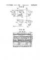
- FIG. 1is a perspective view of a first embodiment of the liquid crystal display device of the present invention
- FIG. 2is an equivalent circuit diagram of this embodiment
- FIG. 3is a schematic view of a video projector applying this embodiment
- FIG. 4is a sectional view of a second embodiment
- FIG. 5is an equivalent circuit diagram of the second embodiment
- FIG. 6is a sectional view of a third embodiment
- FIG. 7is an equivalent circuit diagram of the third embodiment
- FIG. 8is a sectional view of a fourth embodiment
- FIG. 9is an equivalent circuit diagram of the fourth embodiment.
- FIG. 10is a sectional view of a fifth embodiment
- FIG. 11is an equivalent cirucit diagram of the fifth embodiment
- FIG. 12is an equivalent circuit diagram of a sixth embodiment
- FIG. 13is a plan view of the sixth embodiment
- FIG. 14is a sectional view of the sixth embodiment
- FIG. 15is a graph showing the characteristics of the liquid crystal for explaining the mode of operation of the sixth embodiment.
- FIG. 16is an equivalent circuit diagram of a seventh embodiment
- FIG. 17is a plan view of the seventh embodiment
- FIG. 18is an equivalent circuit diagram of an eighth embodiment
- FIG. 19is a sectional view of the eighth embodiment.
- FIG. 20is a perspective view of a ninth embodiment
- FIG. 21is a plan view of the selecting line panel of the ninth embodiment.
- FIGS. 22 and 23are sectional views of the ninth embodiment
- FIG. 24is an equivalent circuit diagram of the ninth embodiment.
- FIG. 25is an equivalent circuit diagram of a tenth embodiment.
- FIG. 26is an equivalent circuit diagram of an eleventh embodiment.
- FIG. 1is a perspective view illustrating the construction of a first embodiment.
- LSI circuit array 12On a reinforcing plate 10 are disposed an LSI circuit array 12, a dielectric mirror 14, a seal 16, a transparent electrode 18, and a glass plate 20 in the order named.
- Liquid crystal 22is sealed by the seal 16 between the dielectric mirror 14 and the transparent electrode 18.
- an alignment film to determine the electric field orientation of the liquid crystalis omitted.
- a TN type liquid crystalis preferable for good contrast or for color display, other types of liquid crystals may be used for the liquid crystal 22, e.g. the dynamic scattering (DS) type.
- DSdynamic scattering
- the expression “transparent”, “nontransparent” or “transmittance “0"/"1””denotes the condition of a liquid crystal observal via a polarizer, when it comes to a liquid crystal in which only the molecular arrangement is changed by the application of an electric field like a TN type liquid crystal.
- An AC power source 24is connected to a substrate of the LSI circuit array 12 and the transparent electrode 18.
- FIG. 2is an equivalent circuit diagram of the first embodiment.
- This LSI circuit array 12has I ⁇ J cells 12-11, . . . 12-IJ, and the liquid crystal 22 is controlled for each picture element corresponding to these cells. Since the construction of these cells 12-11, . . . 12-IJ is the same, the description will only refer to the cell 12-11, and the description of the other cells will be omitted.
- N-channel depletion type MOS FETs 28 and 30 and N-channel enhancement type MOS FETs 32 and 34are so connected to comprise a flip-flop circuit. The following description will be made on the assumption that the MOS FETs are all of n-channel type. Drains of the MOS FETs 28 and 30 are connected to a power source terminal Vcc.
- Sources of the MOS FETs 32 and 34are grounded.
- a source of the MOS FET 28is connected to a drain of a MOS FET 36
- a source of the MOS FET 30is connected to a gate of a MOS FET 38
- a source of the MOS FET 36is connected to a data terminal 42-1 through a data line 40-1.
- a gate of the MOS FET 36is connected to an address terminal 46-1 through a selection line 44-1. All the cells in one column are connected to the same data line 40, and all the cells in one row are connected to the same selection line 44.
- a drain of the MOS FET 38is connected to an aluminum electrode 48.
- the aluminum electrode 48is connected to one end of the AC power source 24 through the liquid crystal 22 and the transparent electrode 18. The other end of the AC power source 24 is grounded.
- the data terminal 42 and the address terminal 46are connected to a shift register, a selection gate and the like.
- the AC voltage applied to this liquid crystal 22is small, the molecular orientation of the liquid crystal does not change, and the liquid crystal is still nontransparent.
- the data terminal 42is at L level, the condition of the flip-flop circuit is inverted, rendering the MOS FET 38 conductive.
- the AC voltage applied to the liquid crystal 22is great this time, the molecular orientation of the liquid crystal 22 is changed, and the liquid crystal becomes transparent.
- the address terminal 46When writing of the data for one row is terminated, the address terminal 46 is placed at the ground level again. After the data terminals 42-1, . . . 42-J set for the level corresponding to the picture image of the next row, the address terminal 46 of the next row is set at the writing level. In the cell where the address terminal 46 is set at the ground level, the condition of the flip-flop circuit does not change independently of the level of the data terminal 42. That is, the picture image data is stored. When writing of the data in all the cells is completed, all the data terminals 42-1, . . . 42-J and the address terminals 46-1, . . . 46-I are set at the ground level, the molecular orientation of the liquid crystal is made stationary according to the written picture image data, and the liquid crystal displays the picture image.
- all the data terminals 42-1, . . . 42-Jare set at H level and all the address terminals 46-1, . . . 46-I are set at the writing level. Then, the MOS FETs of all the cells are rendered nonconductive. Similar to the case of writing the data, when the data terminal 42 is set at H level and a desired address terminal 46 alone is set at the writing level, the data of a desired cell alone may be erased.
- the liquid crystal elementit is possible to arrange memory cells corresponding to each picture element for the liquid crystal element itself so that the liquid crystal may be controlled for each picture element according to the stored data in the memory cells, thereby providing a display device of high resolution. Since these memories comprise LSI circuits, they may be less expensive and simpler in construction. In a general refresh type memory having no storing capability, the data must be read out from the memory every 20 msec or so. However, since the time required for displaying one picture image is as long as about several hundred msec, sufficient writing speed of the data to the memory may be realized by the present LSI techniques. With picture image data memories, random defective memories at a rate of about 1/1,000 to 1/10,000 picture elements are practically negligible, unlike the case of semiconductor memories. It is to be noted that the mode of operation of the embodiment is similar when p-channel type MOS FETs are used.
- FIG. 3shows the optical system of the slide projector applying the liquid crystal display device of this embodiment as a video valve.
- the light emitted from a light source 48is incident on a polarizing spectroscope 52 through a lens 50.
- the polarizing spectroscope 52has a polarization plane. When the molecular orientation of the liquid crystal does not coincide with the orientation of the polarizing plane, the polarizing spectroscope 52 does not transmit light and is dark. When the molecular orientation of the liquid crystal coincides with the orientation of the polarizing plane, it transmits light and becomes brighter.
- the output light of the polarizing spectroscope 52is enlarged by a lens 56 and is displayed on a screen 58.
- a spectroscopemay be used in place of a polarizing spectroscope.
- the data of each cellmay be read out through the data line 40 by setting the address terminal 46 at a voltage exceeding the threshold voltage, thereby rendering the MOS FET 36 conductive.
- the devicemay also be used as a memory device for the picture image filing, the data filing, or electronically editing the picture images.
- the LSI circuit array of this embodimenthas elements which number as many as 6 per cell, so that the yield of the production of the LSI circuit is not very high. Furthermore, the stored data of the flip-flop circuit may be erased by a momentary power failure.
- an LSI circuit array 12comprise nonvolatile memory transistors.
- the nonvolatile memory transistorsmay include metal insulator semiconductor (MIS) type memory transistors, floating gate type memory transistors or ferroelectric memory transistors.
- the MIS type elementsmay include, for example, metal nitride oxide semiconductor (MNOS) transistors, metal alumina oxide semiconductor (MAOS) transistors and dual dielectric charge storage cells (DDC).
- the floating gate type transistorsmay include, for example, floating gate avalanche injection MOS (FAMOS) and stacked gate avalanche injection MOS (SAMOS).
- FIG. 4is a sectional view and FIG. 5 is an equivalent circuit diagram of a liquid crystal display device which uses p-channel MNOS FETs as nonvolatile memory transistors.
- an n-type monocrystalline silicon substrate 62is laminated over a plastic reinforcing plate 10.
- P + -type semiconductor regions 64 and 66are formed for each cell in the surface area of an n-type substrate 62.
- a silicon oxide layer 68 and a coating layer 70are formed on the n-type substrate 62 in the order named.
- Aluminum electrodes 48are formed on a p + -type semiconductor regions 66, and these aluminum electrodes 48 reach the coating layer 70.
- Nitride layers 72are formed through the oxide layer 68, on the n-type substrate 62 between the p + -type semiconductor regions 64 and 66, and polycrystalline silicon layers 74 are formed thereover.
- the thickness of the nitride layer 72is, e.g. 400 ⁇
- the thickness of the oxide layer 68 interposed between the nitride layer 72 and the n-type substrate 62is, e.g. 20 ⁇ .
- the p + -type semiconductor regions 64 and 66comprise a source region and a drain region, respectively
- the polycrystalline silicon layer 74comprises a gate region.
- the nitride layer 72 interposed between the oxide layer 68 and the polycrystalline silicon layer 74is very thin so that exchange of electrons with the n-type substrate 62 is possible by the tunnel effect, thus providing an insulation layer for trapping electrons.
- the regions from the n-type substrate 62 to the coating layer 70comprise the LSI circuit array 12.
- the dielectric mirror 14, the liquid crystal 22, the transparent electrode 18, and the glass plate 20are formed on the coating layer 70 in the order named.
- each LSI circuit cellcomprises a p-channel MNOS FET 76, a gate of which is connected to an address terminal 46 through a selection line 44, a source of which is connected to a data terminal 42 through a data line 40 and a drain of which is connected to the aluminum electrode 48.
- the selection line 44is arranged in the direction of column so that writing is performed for each column. It is assumed that all the MNOS FETs 76 are conductive, the electrons are trapped in the nitride layer 72 below the gate region, and a channel is formed between the source and drain regions.
- the data terminals 42are set at the ground level or a suitable negative level (e.g., -20 V) according to the picture image of the column to be written. Then, the address terminal 46 of the column to be written alone is set at a suitable writing level (e.g., -25 V).
- the electrons trapped in the nitride layer 72are freed into the substrate 62, rendering the MNOS FET 76 nonconductive.
- the electronsare not released into the substrate 62, the MNOS FET 76 remains conductive.
- the MNOS FET 76In a cell in which the MNOS FET 76 is rendered nonconductive, when the floating capacitance between the drain of the MNOS FET 76 and the substrate 62 is about equal to or less than the capacitance between the aluminum electrode 48 and the transparent electrode 18, the molecular orientation of the liquid crystal 22 does not change. In a cell in which the MNOS FET 76 remains conductive, the AC voltage is kept applied so that the molecular orientation of the liquid crystal 22 changes. Thus, the picture image data is written. After the data for one column is written, its address terminal 46 is set at the ground level, and the address terminal of another column is set at the writing level.
- the condition of the electrons in the nitride layerdoes not change independently of the level of the data terminal 42, so that the written data remains stored.
- all the data terminals 42 and the address terminals 46are held at the ground level, and the molecular orientation of the liquid crystal 22 is fixed according to the data written.
- all the address terminals 46are set at a suitable negative erasing level (e.g., -25 V). Then, the electrons are trapped in the nitride layers 72 below the gate regions 74 of all the cells, and all the MNOS FETs 76 are rendered conductive.
- a suitable negative erasing levele.g., -25 V
- the yield of the LSI circuit array 12is improved. Furthermore, since nonvolatile memory transistor is used, the data is not erased even in the case of a momentary power failure.
- FIG. 6is a sectional view of a third embodiment
- FIG. 7is an equivalent circuit diagram of this embodiment.
- each LSI circuit cellcomprises two variable capacitors.
- the capacitorcomprises a substrate 62 and gate region 74 of the p-type MNOS FET of the second embodiment, excluding a source and drain.
- the region of the n-type substrate 62 where the channel is formed, that is, a data line 40,is an n + -type semiconductor.
- a polycrystalline silicon layer 74constitutes a selection line 44, and a nitride layer 72 interposed between an oxide layer 68 and the polycrystalline silicon layer 74 constitutes an insulation layer for trapping electrons.
- a sapphire substrate 78is formed on a reinforcing plate 10, and the n-type substrate 62 corresponding to the respective cell is formed on the sapphire substrate 78.
- each cellcomprises two variable capacitors 80 and 82.
- One end of the capacitor 80is connected to one end of the capacitor 82 and to a data terminal 42 through a data line 40.
- the other end of the capacitor 80is connected to an address terminal 46 through a selection line 44.
- the other end of the capacitor 82is connected to an aluminum electrode 48.
- the depletion layerdoes not extend to the n-type substrate 62 unless a high electric field is applied to both its ends.
- the capacitance of the capacitor 80 between the n-type substrate 62 and the polycrystalline silicon layer 74, i.e., the data line 40 and the selection line 44becomes great.
- the capacitance of the capacitor 82 between the data line 40 and the aluminum electrode 48also becomes great. For this reason, an AC voltage is applied to the liquid crystal 22, and the liquid crystal 22 becomes transparent.
- the data terminal 42is set at a suitable negative level, the electrons in the nitride layer 72 are not released and remain trapped.
- the depletion layerextends into the n-type substrate 62 unless a high electric field is applied to both ends of the capacitor.
- the capacitances of the capacitors 80 and 82are small. For this reason, an AC voltage is not applied to the liquid crystal 22 so that the liquid crystal is nontransparent.
- the address terminal of this columnWhen writing of the data for one column is completed, the address terminal of this column is set at the ground level, and the address terminal of another column is set at the writing level. In a cell in which the address terminal 46 is set at the ground level, the condition of the electrons in the insulation layer 72 does not change independently of the level of the data terminal 42. For this reason, the written data is retained. When the writing of the data in all the cells is completed, all the address terminals 46 and the data terminals 42 are set at the ground level, and the molecular orientation of the liquid crystal is made stationary according to the written data.
- the aluminum electrode 48is at a floating DC voltage, static electricity is applied and the trapping and release of the electrons in and from the insulation layer may be obstructed.
- the resistive coating layer 70is used, the static electricity charged on the aluminum electrode 48 is naturally discharged.
- the stored datawill not be erased by a momentary power failure. Furthermore, since there is no p-n junction, the construction is simple and the yield of the LSI circuit array is vastly improved.
- the datais kept stored based on the capacitance according to the presence or absence of depletion layers in the substrate, i.e., the presence or absence of a minority carriers at the surface of the substrate.
- a large AC electric fieldis applied to drive the liquid crystal 22 under the condition that the depletion layers are widely extended, holes are induced at the surface of the substrate at every negative half-cycle of the AC electric field. This may vary the capacitance.
- a p + -type data linein place of the n + -type data line 40. That is, it suffices to form the source of the MNOS FET alone and to keep the data stored according to the variations in the capacitance between the gate and the source which depends upon the presence or absence of the channel layer at the surface of the substrate.
- the capacitancein this case, is large when the electrons are trapped in the insulation layer, and is small when the electrons are not trapped in the insulation layer, unlike in the former case. Since the writing or erasing of the data may be performed in a manner similar to the former embodiment, the description thereof will be omitted.
- FIG. 8is a sectional view of a fourth embodiment
- FIG. 9is an equivalent circuit diagram for this embodiment.
- p + -type regions 86 corresponding to each cellare formed at the surface area of an n-type substrate 62
- n + -type regions 88are formed at the surface areas of the p + -type regions 86.
- An oxide layer 68 and a coating layer 70are formed on the n-type substrate 62 in the order named.
- Aluminum electrodes 48 and chalcogen type amorphous semiconductor layers 90are formed on the n + -type regions 88. One end of each amorphous layer 90 is in contact with a respective aluminum electrodes 48.
- Polycrystalline silicon layers 74are formed on the amorphous layers 90.
- each cellcomprises a diode 92 and a variable resistor 94.
- An anode of the diode 92consisting of the p + -type region 86 and the n + -type region 88 is connected to an address terminal 46 through a selection line 44.
- a cathode of the diode 92is connected to the aluminum electrode 48.
- One end of a variable resistor 94consisting of the amorphous layer 90 is connected to the aluminum electrode 48, and the other end thereof is connected to a data terminal 42 through a data line 40.
- the polycrystalline silicon layers 74constitute the data lines 40.
- the chalcogen type amorphous semiconductorsundergo phase transition and their resistances change when a suitable pulse voltage or a pulse current is applied. It is assumed that all the variable resistors 94 are under high resistance condition and an AC voltage is not substantially applied to the liquid crystal 22 in the initial state.
- the data terminals 42-1 to 42-Iare set at the ground level on a suitable positive level VS according to the data to be written.
- a writing pulse of a suitable shape having a suitable positive level of VW (VW>VS) as the pulse heightis supplied to one of the address terminals 46.
- the amorphous semiconductor 90undergoes phase transistion, the variable resistor 94 has a low resistance, and an AC voltage is applied to the liquid crystal 22.
- the amorphous semiconductor 90does not undergo phase transition and the variable resistor 94 remains to have a high resistance.
- the associated address terminal 46is set at the ground level, and the writing pulse is supplied to another address terminal.
- the amorphous semiconductor 90does not undergo phase transition independently of the data terminal 42 and the written data remains stored. After writing in all the cells, all the address terminals 46 and the data terminals 42 are set at the ground level, and the molecular orientation of the liquid crystal 22 remains under the condition corresponding to the written data.
- an erasing pulse of a suitable shape and of a suitable positive pulse heightis supplied to all the address terminals 46-1 to 46-J. Then, the amorphous semiconductor 90 having a low resistance undergoes phase transition so that all the variable resistors 94 have a high resistance.
- an erasing pulseis supplied to any selected address terminal 46 after placing the data terminals 42 under grounded or open condition, the data of this cell alone may be erased.
- the datamay be retained in the case of a momentary power failure. Furthermore, as in the case of the first embodiment which utilizes flip-flop circuits, the written data may be read out through the selection line 44 and the data line 40 to be used as the picture image file.
- FIG. 10is a sectional view of a fifth embodiment.
- a first n + -type region 100, a second n + -type region 102 and a third n + -type region 104are formed for one cell in the surface area of an n-type substrate 62.
- a p-type region 106is formed in the surface area of the third n + -type region 104.
- Ion-implanted parts 108 and 109are respectively formed in the surface area of the n-type substrate 62 between the first and second n + -type regions 100 and 102 and between the second and third n + -type regions 102 and 104.
- An aluminum electrode 48is formed on the second n + -type region 102.
- Part of an oxide layer 68is cut away to form a window 110 to receive light at the upper part of the third n + -type region 104, and a coating layer 70 is in direct contact with the third n + -type region 104.
- Low-resistance polycrystalline silicon layers 112 and 114are formed in the oxide layer 68 above the ion- implanted parts 108 and 109, respectively.
- the low resistance polycrystalline silicon layers 112 and 114are connected by a high resistance polycrystalline silicon layer 116. Part of the low resistance polycrystalline silicon layer 114 is in contact with the p-type region 106 and the coating layer 70.
- FIG. 11A circuit diagram of the equivalent circuit of this embodiment is shown in FIG. 11.
- Each cellcomprises two depletion type n-channel MOS FETs 120 and 122, a high resistance resistor 124 and a photodiode 126.
- Sources and drains of the MOS FETs 120 and 122are connected to each other to comprise an OR gate.
- a gate of the MOS FET 120is connected to a data terminal 42 through a data line 40.
- Drains of the MOS FETs 120 and 122are connected to an aluminum electrode 48, and sources thereof are connected to an address terminal 46 through a selection line 44.
- a gate of the MOS FET 122is connected to an anode of the photodiode 126 as well as to the gate of the MOS FET 120 through the resistor 124.
- a cathode of the photodiode 126is connected to the address terminal 46 through a selection line 44.
- the low resistance polycrystalline silicon layer 112, the first n + -type region 100 and the second n + -type region 102respectively constitute the gate, source and drain of the MOS FET 120.
- the low resistance polycrystalline silicon layer 114, the third n + -type region 104 and the second n + -type region 102respectively constitute the gate, source and drain of the MOS FET 122.
- the third n + -type region 104 and p-type region 106constitute the photodiode 126, and the high resistance polycrystalline silicon layer 116 constitutes the resistor 124.
- the MOS FETs 120 and 122are turned into the depletion type by the ion-implanted layers 108 and 109.
- the MOS FETs 120 and 122are rendered conductive since they are of depletion type, an AC voltage is applied to the liquid crystal 22, and the liquid crystal 22 becomes transparent and transmits light. Thus, the light becomes incident on the photodiode 126 through the window 110, rendering the photodiode 126 conductive. Then, the biasing voltage V1 of the address terminal 46 is applied to the MOS FET 122 through the selection line 44 and the photodiode 126, and the MOS FET 122 remains conductive thereafter.
- the MOS FET 120remains nonconductive and the liquid crystal 22 remains nontransparent.
- the address terminal 46 for this rowis set at the ground level, and the address terminal of another row is set at the V1 level.
- the condition of the MOS FET 120does not change independently of the level of the data terminal 42 so that the data remains stored.
- light and a logic circuitconstitute a flip-flop circuit, so that a smaller number of logic circuit may comprise an LSI circuit array.
- the number of times for writing datais limited in the embodiment wherein the nonvolatile memories such as the MNOS FETs or the amorphous semiconductors are used, such limits are not imposed on this embodiment since it employs flip-flop circuits.
- the MOS FET 120 and 122constituted an OR gate
- the MOS FETsmay instead comprise an AND gate if the initial condition of the liquid crystal when no electric field is applied is to be suitably set and the MOS FET is of the enhancement type.
- one memory cellwas arranged for one picture element.
- a descriptionwill now be made with reference to a case wherein one memory cell is arranged for several picture elements in order to reduce the number of cells to be packaged on the LSI circuit array 12.
- FIG. 12is a circuit diagram of the equivalent circuit of a sixth embodiment.
- the basic construction of the memory cellsis similar to that of the second embodiment shown in FIG. 5, and one cell comprises one p-channel MNOS FET 76.
- the transparent electrode 18is adhered on the entire surface of the glass plate 20 in the above embodiments, two kinds of comb-shaped transparent electrodes 130 and 132 are combined as seen from the plan view of FIG. 13.
- the transparent electrodes 130 and 132are respectively connected to AC power sources 134 and 136.
- the two transparent electrodes 130 and 132are arranged above one aluminum electrode 48.
- the address terminal 46 of the column to be written aloneis set at the negative writing level (e.g., -25 V).
- the negative writing levele.g., -25 V.
- the data terminal 42is set at the ground level
- the electrons trapped in the insulation layerare released into the substrate, rendering the MNOS FET 76 nonconductive.
- the data terminal 42is set at the V3 level
- the electrons trapped in the insulation layerare not released in the substrate and the MNOS FET 76 remains saturated.
- the data terminal 42is set at the V2 level
- the electrons trapped in the insulation layerare released into the substrate by a small amount, and the MNOS FET 76 remains conductive although not saturated.
- the electrons trapped in the insulation layerare released into the substrate more than in the case wherein the data terminal 42 is set at the V2 level. Then, although the MNOS FET 76 is not rendered nonconductive, it is rendered conductive with considerable on resistance.
- the condition of the MNOS FET 76 of each cellis determined according to the level of the data terminal 42.
- the parts between the gates and the sources of the respective MNOS FETs 76are set at substantially no electric field.
- a suitable AC voltage VR0is applied to all the data terminals 42-1 to 42-I, and AC voltages VR1 and VR2 (VR0, VR1 and VR2 are synchronized each other and their effective values are different) are applied across the transparent electrodes 130 and 132 to the liquid crystal 22 by the AC power sources 134 and 136, respectively. It is assumed that, as shown in FIG. 15, the liquid crystal 22 is at the level of "0" in transmittance and is nontransparent when the applied AC electric field is at the level of "1” or less and it is at the level of "1" in transmittance and is transparent when the AC electric field is above the level of "2".
- the transmittances of the liquid crystals interposed between the aluminum electrode 48 and the transparent electrodes 130 and 132, respectivelybecome at the levels of "0" and "1” so that they become nontransparent and transparent, respectively.
- the transmittances of the liquid crystalsbecome (nontransparent and nontransparent), (transparent and nontransparent), and (transparent and transparent). Since erasing of the data may be performed in the similar manner to that described hereinabove referring to FIG. 5, the description thereof will be omitted.
- the intermediate values as well as the two values of on and offare stored in the nonvolatile memory transistor, the transparent electrode sandwiching the liquid crystal together with the aluminum electrode is divided into two, and different AC voltages are applied to each of them, so that the liquid crystal for 2 picture elements may be controlled with one aluminum electrode, i.e., one memory cell.
- the number of the cells packaged on the substratemay be reduced to half that of the picture elements, that is, to a desired resolution, the yield of the LSI circuit array may further be improved, and the resolution may be improved.
- FIG. 16is an equivalent circuit diagram of a seventh embodiment.
- the memory cellscomprises p-channel MNOS FETs as in the case of the sixth embodiment.
- three transparent electrodes 140, 142, and 144are disposed for one aluminum electrode 48.
- AC power sources 146, 148 and 150are respectively connected to the three transparent electrodes 140, 142, and 144.
- FIG. 17shows the arrangement of the aluminum electrode 48 and the transparent electrodes 140, 142 and 144.
- the liquid crystals between the aluminum electrode and the transparent electrodesbecome (nontransparent, nontransparent and transparent), (nontransparent, nontransparent and nontransparent), (transparent, nontransparent and nontransparent), (transparent, transparent and nontransparent) and (transparent, transparent and transparent).
- two other conditions of (transparent, nontransparent, and transparent) and (nontransparent, transparent, and nontransparent)may be considered in addition to these six conditions, these cannot be realized in this embodiment.
- the condition of (transparent, nontransparent and transparent)may be practically considered to be the same as the condition of (transparent, transparent and transparent).
- the condition of (nontransparent, transparent and nontransparent)may be considered to be the same as the condition of (nontransparent, nontransparent and nontransparent).
- the number of elements to be packaged on the LSI circuit arraymay be made one third of the number of the picture elements, facilitating a further improvement in the packaging density, yield, and resolution.
- Construction including a plurality of transparent electrodes for controlling a plurality of picture elements with one memory cellis not limited to the p-channel MNOS FET cell alone but may be applied to all of the first and the third to the fifth embodiments described hereinabove. For example, as shown in FIG. 7, a case will be described in which variable capacitors comprise cells.
- FIG. 18is an equivalent circuit diagram of an eighth embodiment and FIG. 19 is a sectional view thereof.
- Three transparent electrodes 140, 142, and 144are formed on one aluminum electrode 48.
- the plan view of this embodimentis the same as FIG. 17.
- the liquid crystal 22is interposed between alignment films 152 and 154, as shown in FIG. 19.
- the address terminal of the column to be writtenis set to a suitable negative writing level (e.g., -25 V).
- a suitable negative writing levele.g., -25 V.
- the capacitances of the capacitors 80 and 82are great and they are conductive with a small AC impedance.
- the data terminal 42is set at -20 V
- only a small number of electrons trapped in the nitride layer 72are released so that the capacitors 80 and 82 remain nonconductive.
- the AC impedanceis smaller for the cell with the data terminal 42 of a higher level (closer to the ground level).
- a suitable AC voltage(of the same phase as the AC voltage which is applied to the transparent electrodes 140, 142, and 144) is applied to all the data terminals 42-1 to 42-I.
- the liquid crystal 22 between the aluminum electrode 48 and the transparent electrodes 140, 142, and 144is controlled as in Table 2.
- FIG. 20is a perspective view of a ninth embodiment.
- a dielectric mirror 202, an alignment film 204, a seal 206, an alignment film 208, and a selection line panel 210are formed in the order named on a data line panel 200 comprising nonvolatile memory elements arranged in a matrix form (e.g., 2,000 ⁇ 2,000) and electrodes connected to the respective elements.
- Liquid crystal 212is interposed between the alignment films 204 and 208, and is sealed by the seal 206.
- FIG. 21is a plan view of the selection panel 210. It is assumed that the data line panel 200 has 5 ⁇ 5 nonvolatile memory cells for the sake of simplicity. Twenty-five transparent electrodes 214 are arranged parallel to each other on a glass base plate (not shown). One end of each transparent electrode 214 is connected to a transistor 216 arranged in a matrix form of 5 ⁇ 5. The transistor 216 is made of amorphous silicon and is formed on a glass base plate. The transistors 216 of each column and row are connected to connecting pads 220 through connecting wires 218.
- FIG. 22is a sectional view in the direction perpendicular to the transparent electrodes 214
- FIG. 23is a sectional view in the direction parallel to the transparent electrodes 214.
- a sapphire substrate 224is adhered on a reinforcing plate 222.
- a plurality (2,000) of rodlike n-type semiconductor substrates 226are arranged on the sapphire substrate 224 in the direction perpendicular to the transparent electrodes 214.
- N + -type regions 228are formed in the surface areas of the n-type substrates 226 to extend along the n-type substrates 226, i.e., in the direction perpendicular to the transparent electrodes 214, as shown in FIG. 23.
- An.oxide layer 230is formed on the sapphire substrate 224 and the n-type substrates 226.
- Nitride layers 232extend within each oxide layer 230 on the respective n-type substrates 226 and along the n-type substrates 226.
- Aluminum electrodes 234are formed on the respective nitride layers 232. The upper ends of the aluminum electrodes 234 are exposed from the oxide layer 230. These layers constitute the data line panel 200.
- the dielectric mirror 202is formed on the oxide layer 230 and the aluminum electrodes 234; and the alignment film 204, the liquid crystal 212, the alignment film 208, the transparent electrode 214, and the glass plate 236 are formed thereover in the order named.
- each LSI cellcomprises a variable capacitor 240.
- One end of the liquid crystal 212is connected to an address terminal 244 through a selection line 242 and the other end is connected to one end of the variable capacitor 240 through the aluminum electrode 234.
- the other end of the capacitor 240is connected to a data terminal 248 through a data line 246.
- the transparent electrode 214 of the selection line panel 210constitutes a selection line 242
- the connection pad 220constitutes the address terminal 244
- the n + -type region 228 of the data line panel 200constitutes a data line 246.
- the liquid crystal 212 interposed between the transparent electrode 214 and the aluminum electrodes 234functions as a capacitor of substantially constant capacitance.
- This capacitanceis set such that the trapping of the electrons in the nitride layers 232, that is, writing of the picture image data and the display drive of the liquid crystal 212 may be correctly performed.
- the electronsare trapped in the insulation layers 232 of all the capacitors 240, depletion layers extend into the n-type substrates 226 when no electric field is applied, and the capacitances of the capacitors 240 are at the minimum.
- a suitable threshold voltageis supplied to a predetermined address terminal 244, i.e., the connecting pad 220 for selecting a particular transparent electrode 214, for rendering all the transistors 216 connected to this pad 220.
- All the data terminals 248are set at the ground level or at a suitable negative level Vs according to the data to be written.
- the address terminal 244 of the column to be written aloneis set at the suitable negative writing level.
- the data terminal 248, i.e., the n + -type region 228is set at the ground level, the electrons trapped in the nitride layer 232 are released into the n-type substrate 226.
- the depletion layerdoes not extend into the n-type substrate 226 unless a high electric field is applied to both ends of the capacitor 240, the capacitance of it becomes great.
- the data terminal 248is set at the suitable negative level, the electrons remain trapped so that the capacitance of the capacitor 240 remains small.
- the picture image datais stored in each cell as the capacitance of the capacitors 240.
- an AC voltage for driving the liquid crystal 212is applied across all the address terminals 244 and the data terminals 248. Since the voltage applied to the liquid crystal 212 varies depending upon the capacitances of the capacitors 240, the liquid crystal 212 is controlled for each picture element.
- all the data terminals 248are set at a suitable negative erasing voltage and all the address terminals 244 are set at the ground level. Then, the electrons are trapped in the insulation layers 232 in all the capacitors 240 so that the capacitances of all the capacitors 240 are small. For this reason, substantially no AC voltage is applied to the liquid crystal 212. It is also possible to erase the data of any selected cell alone by setting all the address terminals 244 at a suitable negative level Vs and all the data terminals 248 at a suitable negative level Vs and thereafter setting the selected address terminal 244 at the ground level, in a manner opposite to the case of writing of the data.
- the transparent electrodes and the selection linesare common, the LSI circuit cells with a still simpler construction are realized, improving the yield of the LSI circuit cells.
- the selection panel 210comprises an amorphous silicon transistor or the like on a glass substrate, it may alternatively be of the SOS structure which is formed on a sapphire substrate. Although the SOS structure is more expensive, it allows high speed operation. With the amorpous silicon transistor, high speed operation may also be enabled by monocrystallizing utilizing laser annealing. Although the transistor array on the selection line panel 210 was arranged in two-dimensional manner, the number of connecting wires with the external circuits may further be reduced if decoders are formed, neglecting the increase in the number of elements.
- the present inventionis not limited to this.
- a nonvolatile memory transistors 250are used.
- a source of the transistor 250is connected to a data line 246, and a gate and drain thereof are connected to an aluminum electrode 234.
- the sectional views of this embodimentwill be the same as those shown in FIGS. 22 and 23 except that the transistor 250 is formed in the n-type substrate 226. Writing and erasing of the data is performed depending upon whether or not the electrons are trapped in the insulation layers below the gates of the transistors 250 in this embodiment as in the former embodiments. However, the difference is that the drive control of the liquid crystal 212 is performed according to the conductive or nonconductive condition of the transistors 250.
- FIG. 26shows a circuit diagram of the equivalent circuit of the embodiment where one cell comprising a variable capacitor 240 controls two picture elements. Since the plan view of this embodiment is the same as FIG. 13, it will be omitted.
- An aluminum electrode 234is connected to selection lines (transparent electrodes) 252 and 254 through a liquid crystal 212, and the selection lines 252 and 254 are connected to address terminals 256 and 258, respectively.
- the mode of operation of this embodimentis similar to the mode of operation of the embodiment described with reference to FIGS. 12 to 15, the description of it will be omitted.
- the datawas stored as the on resistance of the MNOS FET in the former embodiment, the data is stored as the capacitance of the capacitor in this embodiment.
- the present inventionis not limited to the particular embodiments described above and various other modifications and variations can be made without departing the spirit and scope of the present invention.
- the liquid crystal display devicewas used as the light valve, the dielectric mirror may be eliminated and the device may be used as the reflecting type display device as in the case of the liquid crystal TV.
- the nonvolatile memoriesmay comprise the MNOS MoOSs (metal nitride molybdenum oxide semiconductors). By suitably selecting the biasing voltage, it is possible to obtain intermediate display modes in addition to the two modes of transparency and nontransparency.
- the liquid crystal display deviceitself includes a static type memory which has the function to store data and does not require an external memory circuit for this purpose. Although erasing of the stored data is performed at a high speed, it may otherwise be performed with ultraviolet rays as in the case of the ultraviolet ray erasable type programmable ROM if erasing at a high speed is not required.
Landscapes
- Physics & Mathematics (AREA)
- Engineering & Computer Science (AREA)
- Nonlinear Science (AREA)
- General Physics & Mathematics (AREA)
- Chemical & Material Sciences (AREA)
- Crystallography & Structural Chemistry (AREA)
- Optics & Photonics (AREA)
- Mathematical Physics (AREA)
- Computer Hardware Design (AREA)
- Theoretical Computer Science (AREA)
- Microelectronics & Electronic Packaging (AREA)
- Liquid Crystal (AREA)
- Liquid Crystal Display Device Control (AREA)
Abstract
Description
TABLE 1 ______________________________________Liquid Crystal 22Liquid Crystal 22 between Trans- between Trans- Level ofparent Electrode 130parent Electrode 132 Aluminum and Aluminum andAluminum Electrode 48Electrode 48Electrode 48 ______________________________________ 0 0/0 2/1 1 1/0 1/0 2 2/1 0/0 4 4/1 2/1 ______________________________________
TABLE 2 ______________________________________ Liquid Crystal LiquidCrystal Liquid Crystal 22 between 22 between 22 between Level of Transparent TransparentTransparent Aluminum Electrode 140Electrode 142Electrode 144 Electrode and Aluminum and Aluminum andAluminum 48Electrode 48Electrode 48Electrode 48 ______________________________________ 0 1/0 2/1 3/1 1 0/0 1/0 2/1 2 1/0 0/0 1/0 3 2/1 1/0 0/0 4 3/1 2/1 1/0 5 4/1 3/1 2/1 ______________________________________
Claims (19)
Applications Claiming Priority (6)
| Application Number | Priority Date | Filing Date | Title |
|---|---|---|---|
| JP55-20542 | 1980-02-22 | ||
| JP2054280AJPS56117275A (en) | 1980-02-22 | 1980-02-22 | Image display |
| JP9396480AJPS5719785A (en) | 1980-07-11 | 1980-07-11 | Image display unit |
| JP9396280AJPS5719783A (en) | 1980-07-11 | 1980-07-11 | Image display unit |
| JP55-93964 | 1980-07-11 | ||
| JP55-93962 | 1980-07-11 |
Publications (1)
| Publication Number | Publication Date |
|---|---|
| US4432610Atrue US4432610A (en) | 1984-02-21 |
Family
ID=27283090
Family Applications (1)
| Application Number | Title | Priority Date | Filing Date |
|---|---|---|---|
| US06/235,995Expired - Fee RelatedUS4432610A (en) | 1980-02-22 | 1981-02-19 | Liquid crystal display device |
Country Status (3)
| Country | Link |
|---|---|
| US (1) | US4432610A (en) |
| EP (1) | EP0034796B1 (en) |
| DE (1) | DE3176454D1 (en) |
Cited By (74)
| Publication number | Priority date | Publication date | Assignee | Title |
|---|---|---|---|---|
| US4531061A (en)* | 1982-07-01 | 1985-07-23 | Jacob Rabinow | Electrically settable escort memory |
| US4574282A (en)* | 1983-03-18 | 1986-03-04 | International Standard Electric Corporation | Coherent light image generation |
| US4601537A (en)* | 1984-01-06 | 1986-07-22 | Ohio State University Research Foundation | Apparatus and methods for forming images and for optical demultiplexing |
| US4699469A (en)* | 1985-04-17 | 1987-10-13 | International Business Machines Corporation | Liquid crystal display |
| WO1989002144A1 (en)* | 1987-08-27 | 1989-03-09 | Hughes Aircraft Company | Active matrix cell for ac operation |
| US4836655A (en)* | 1986-02-17 | 1989-06-06 | Semiconductor Energy Laboratory Co., Ltd. | Ferroelectric liquid crystal device with a charge storage structure |
| US4846559A (en)* | 1986-01-30 | 1989-07-11 | Messerschmitt Bclkow-Blohm GmbH | Sensor element with a memory for abnormal changes of the incident light intensity |
| US4846557A (en)* | 1986-11-05 | 1989-07-11 | Commissariat A L'energie Atomique | Matrix display device and process for controlling said device |
| US4973135A (en)* | 1984-08-22 | 1990-11-27 | Shinjiro Okada | Active matrix display panel having plural stripe-shaped counter electrodes and method of driving the same |
| US5151805A (en)* | 1989-11-28 | 1992-09-29 | Matsushita Electric Industrial Co., Ltd. | Capacitively coupled driving method for TFT-LCD to compensate for switching distortion and to reduce driving power |
| US5317433A (en)* | 1991-12-02 | 1994-05-31 | Canon Kabushiki Kaisha | Image display device with a transistor on one side of insulating layer and liquid crystal on the other side |
| US5325220A (en)* | 1993-03-09 | 1994-06-28 | Research Frontiers Incorporated | Light valve with low emissivity coating as electrode |
| WO1994020949A1 (en)* | 1993-03-01 | 1994-09-15 | Wah-Iii Technology Corp. | Polysilicon gate bus with interspersed buffers |
| US5459592A (en)* | 1992-04-24 | 1995-10-17 | Sharp Kabushiki Kaisha | Projection display system including a collimating tapered waveguide or lens with the normal to optical axis angle increasing toward the lens center |
| US5471225A (en)* | 1993-04-28 | 1995-11-28 | Dell Usa, L.P. | Liquid crystal display with integrated frame buffer |
| US5537234A (en)* | 1993-01-19 | 1996-07-16 | Hughes Aircraft Company | Relective liquid crystal display including driver devices integrally formed in monocrystalline semiconductor layer and method of fabricating the display |
| US5576737A (en)* | 1993-12-22 | 1996-11-19 | Seiko Epson Corporation | Liquid crystal drive device, liquid crystal display device, and liquid crystal drive method |
| US5627557A (en)* | 1992-08-20 | 1997-05-06 | Sharp Kabushiki Kaisha | Display apparatus |
| US5633182A (en)* | 1991-12-02 | 1997-05-27 | Canon Kabushiki Kaisha | Method of manufacturing an image display device with reduced cell gap variation |
| US5790213A (en)* | 1994-09-08 | 1998-08-04 | Sharp Kabushiki Kaisha | Image display device having adjacent pixel overlapping circuit elements |
| US5821559A (en)* | 1991-02-16 | 1998-10-13 | Semiconductor Energy Laboratory Co., Ltd. | Electric device, matrix device, electro-optical display device, and semiconductor memory having thin-film transistors |
| US5838308A (en)* | 1991-04-17 | 1998-11-17 | U.S. Philips Corporation | Optical touch input device |
| US5844538A (en)* | 1993-12-28 | 1998-12-01 | Sharp Kabushiki Kaisha | Active matrix-type image display apparatus controlling writing of display data with respect to picture elements |
| US5920298A (en)* | 1996-12-19 | 1999-07-06 | Colorado Microdisplay, Inc. | Display system having common electrode modulation |
| US5959598A (en)* | 1995-07-20 | 1999-09-28 | The Regents Of The University Of Colorado | Pixel buffer circuits for implementing improved methods of displaying grey-scale or color images |
| US6046716A (en)* | 1996-12-19 | 2000-04-04 | Colorado Microdisplay, Inc. | Display system having electrode modulation to alter a state of an electro-optic layer |
| US6072454A (en)* | 1996-03-01 | 2000-06-06 | Kabushiki Kaisha Toshiba | Liquid crystal display device |
| US6078303A (en)* | 1996-12-19 | 2000-06-20 | Colorado Microdisplay, Inc. | Display system having electrode modulation to alter a state of an electro-optic layer |
| US6115019A (en)* | 1998-02-25 | 2000-09-05 | Agilent Technologies | Register pixel for liquid crystal displays |
| US6175351B1 (en) | 1993-08-10 | 2001-01-16 | Sharp Kabushiki Kaisha | Image display apparatus and a method for driving the same |
| US6246386B1 (en)* | 1998-06-18 | 2001-06-12 | Agilent Technologies, Inc. | Integrated micro-display system |
| US6262703B1 (en) | 1998-11-18 | 2001-07-17 | Agilent Technologies, Inc. | Pixel cell with integrated DC balance circuit |
| US6326642B1 (en) | 1992-05-29 | 2001-12-04 | Semiconductor Energy Laboratory Co., Ltd. | Electric device, matrix device, electro-optical display device, and semiconductor memory having thin-film transistors |
| US20020018029A1 (en)* | 2000-08-08 | 2002-02-14 | Jun Koyama | Electro-optical device and driving method of the same |
| US20020021274A1 (en)* | 2000-08-18 | 2002-02-21 | Jun Koyama | Liquid crystal display device, method of driving the same, and method of driving a portable information device having the liquid crystal display device |
| US20020024485A1 (en)* | 2000-08-08 | 2002-02-28 | Jun Koyama | Liquid crystal display device and driving method thereof |
| US20020024054A1 (en)* | 2000-08-18 | 2002-02-28 | Jun Koyama | Electronic device and method of driving the same |
| US20020036613A1 (en)* | 2000-09-18 | 2002-03-28 | Ryoichi Yokoyama | Display device and its driving method |
| US20020036604A1 (en)* | 2000-08-23 | 2002-03-28 | Shunpei Yamazaki | Portable information apparatus and method of driving the same |
| US20020041266A1 (en)* | 2000-10-05 | 2002-04-11 | Jun Koyama | Liquid crystal display device |
| US20020097215A1 (en)* | 2001-01-22 | 2002-07-25 | Huang Samson X. | Pseudo static memory cell for digital light modulator |
| US20020129098A1 (en)* | 2001-03-06 | 2002-09-12 | Dennis Stone | LAN connection status display |
| US20030090478A1 (en)* | 1995-07-20 | 2003-05-15 | The Regents Of The University Of Colorado | Pixel buffer circuits for implementing improved methods of displaying grey-scale or color images |
| US20030098875A1 (en)* | 2001-11-29 | 2003-05-29 | Yoshiyuki Kurokawa | Display device and display system using the same |
| GB2383886A (en)* | 2001-12-20 | 2003-07-09 | Corning Inc | Reflective spatial light modulator comprising dielectric layer/mirror |
| US6600472B1 (en)* | 1998-03-19 | 2003-07-29 | Kabushiki Kaisha Toshiba | Liquid crystal display device |
| US20030169218A1 (en)* | 1998-03-18 | 2003-09-11 | Seiko Epson Corporation | Transistor circuit, display panel and electronic apparatus |
| US20030234755A1 (en)* | 2002-06-06 | 2003-12-25 | Jun Koyama | Light-emitting device and method of driving the same |
| US20040041761A1 (en)* | 2002-08-09 | 2004-03-04 | Tatsuya Sugita | Image display apparatus and image display module |
| US20040125090A1 (en)* | 2002-12-26 | 2004-07-01 | Elcos Microdisplay Technology, Inc. | Method and device for driving liquid crystal on silicon display systems |
| US6781566B2 (en)* | 2001-08-22 | 2004-08-24 | Aurora Systems, Inc. | Residual DC bias correction in a video imaging device |
| US20040222955A1 (en)* | 2001-02-09 | 2004-11-11 | Semiconductor Energy Laboratory Co., Ltd. A Japan Corporation | Liquid crystal display device and method of driving the same |
| US20040258866A1 (en)* | 2003-06-19 | 2004-12-23 | Hitachi., Ltd. | Image display device |
| US20050190201A1 (en)* | 2002-07-23 | 2005-09-01 | Baer David A. | System and method for providing graphics using graphical engine |
| US20060151792A1 (en)* | 1990-11-26 | 2006-07-13 | Semiconductor Energy Laboratory Co., Ltd. | Electro-optical device and driving method for the same |
| US20060227257A1 (en)* | 2005-04-08 | 2006-10-12 | Samsung Electronics Co., Ltd. | Substrate for a liquid crystal display panel, method of manufacturing the same and liquid crystal display device having the same |
| US7180496B2 (en)* | 2000-08-18 | 2007-02-20 | Semiconductor Energy Laboratory Co., Ltd. | Liquid crystal display device and method of driving the same |
| CN1320391C (en)* | 2003-10-28 | 2007-06-06 | 三洋电机株式会社 | Power supply circuit |
| CN1324357C (en)* | 2003-10-28 | 2007-07-04 | 三洋电机株式会社 | Power supply circuit |
| US20070200861A1 (en)* | 2001-11-30 | 2007-08-30 | Semiconductor Energy Laboratory Co., Ltd. | Display Device and Display System Using the Same |
| US20070287211A1 (en)* | 2006-06-08 | 2007-12-13 | Yi-Tyng Wu | Method of improving the flatness of a microdisplay surface, liquid crystal on silicon (LCoS) display panel and method of manufacturing the same |
| US8106867B2 (en) | 1990-11-26 | 2012-01-31 | Semiconductor Energy Laboratory Co., Ltd. | Electro-optical device and driving method for the same |
| US11538431B2 (en) | 2020-06-29 | 2022-12-27 | Google Llc | Larger backplane suitable for high speed applications |
| US11568802B2 (en) | 2017-10-13 | 2023-01-31 | Google Llc | Backplane adaptable to drive emissive pixel arrays of differing pitches |
| US20230067080A1 (en)* | 2021-08-26 | 2023-03-02 | Samsung Display Co., Ltd. | Display device and manufacturing method of the same |
| US11626062B2 (en) | 2020-02-18 | 2023-04-11 | Google Llc | System and method for modulating an array of emissive elements |
| US11637219B2 (en) | 2019-04-12 | 2023-04-25 | Google Llc | Monolithic integration of different light emitting structures on a same substrate |
| US11710445B2 (en) | 2019-01-24 | 2023-07-25 | Google Llc | Backplane configurations and operations |
| US11768430B2 (en)* | 2015-06-30 | 2023-09-26 | Gauzy Ltd. | Advanced polymer dispersed liquid crystal (PDLC) for display projection screens |
| US11810509B2 (en) | 2021-07-14 | 2023-11-07 | Google Llc | Backplane and method for pulse width modulation |
| US11847957B2 (en) | 2019-06-28 | 2023-12-19 | Google Llc | Backplane for an array of emissive elements |
| US11961431B2 (en) | 2018-07-03 | 2024-04-16 | Google Llc | Display processing circuitry |
| US12107072B2 (en) | 2020-04-06 | 2024-10-01 | Google Llc | Display backplane including an array of tiles |
| US12244786B2 (en) | 2020-12-21 | 2025-03-04 | Google Llc | High density pixel arrays for auto-viewed 3D displays |
Families Citing this family (3)
| Publication number | Priority date | Publication date | Assignee | Title |
|---|---|---|---|---|
| FR2553218B1 (en)* | 1983-10-07 | 1987-09-25 | Commissariat Energie Atomique | ACTIVE MATRIX DISPLAY SCREEN WITHOUT CROSSING LINES AND ADDRESSING COLUMNS |
| NL8801165A (en)* | 1987-06-10 | 1989-01-02 | Philips Nv | APPARATUS FOR PROJECTION TELEVISION. |
| CN107835354B (en)* | 2017-12-15 | 2020-12-18 | 信利光电股份有限公司 | Be applied to electronic equipment's module of making a video recording and electronic equipment |
Citations (8)
| Publication number | Priority date | Publication date | Assignee | Title |
|---|---|---|---|---|
| US3824003A (en)* | 1973-05-07 | 1974-07-16 | Hughes Aircraft Co | Liquid crystal display panel |
| US3910681A (en)* | 1973-01-11 | 1975-10-07 | Marconi Co Ltd | Liquid crystal display devices |
| US4112333A (en)* | 1977-03-23 | 1978-09-05 | Westinghouse Electric Corp. | Display panel with integral memory capability for each display element and addressing system |
| GB2011639A (en)* | 1977-12-28 | 1979-07-11 | Hughes Aircraft Co | Driven liquid crystal light valve |
| GB2016726A (en)* | 1978-03-13 | 1979-09-26 | Hughes Aircraft Co | Interference-reflective electrode for liquid crystal display |
| US4223308A (en)* | 1979-07-25 | 1980-09-16 | Northern Telecom Limited | LCDs (Liquid crystal displays) controlled by thin film diode switches |
| US4233603A (en)* | 1978-11-16 | 1980-11-11 | General Electric Company | Multiplexed varistor-controlled liquid crystal display |
| US4251136A (en)* | 1979-07-25 | 1981-02-17 | Northern Telecom Limited | LCDs (Liquid crystal displays) controlled by thin film diode switches |
- 1981
- 1981-02-17DEDE8181101127Tpatent/DE3176454D1/ennot_activeExpired
- 1981-02-17EPEP81101127Apatent/EP0034796B1/ennot_activeExpired
- 1981-02-19USUS06/235,995patent/US4432610A/ennot_activeExpired - Fee Related
Patent Citations (8)
| Publication number | Priority date | Publication date | Assignee | Title |
|---|---|---|---|---|
| US3910681A (en)* | 1973-01-11 | 1975-10-07 | Marconi Co Ltd | Liquid crystal display devices |
| US3824003A (en)* | 1973-05-07 | 1974-07-16 | Hughes Aircraft Co | Liquid crystal display panel |
| US4112333A (en)* | 1977-03-23 | 1978-09-05 | Westinghouse Electric Corp. | Display panel with integral memory capability for each display element and addressing system |
| GB2011639A (en)* | 1977-12-28 | 1979-07-11 | Hughes Aircraft Co | Driven liquid crystal light valve |
| GB2016726A (en)* | 1978-03-13 | 1979-09-26 | Hughes Aircraft Co | Interference-reflective electrode for liquid crystal display |
| US4233603A (en)* | 1978-11-16 | 1980-11-11 | General Electric Company | Multiplexed varistor-controlled liquid crystal display |
| US4223308A (en)* | 1979-07-25 | 1980-09-16 | Northern Telecom Limited | LCDs (Liquid crystal displays) controlled by thin film diode switches |
| US4251136A (en)* | 1979-07-25 | 1981-02-17 | Northern Telecom Limited | LCDs (Liquid crystal displays) controlled by thin film diode switches |
Non-Patent Citations (11)
| Title |
|---|
| Baraf et al., The Optimization of Metal Insulator Metal Nonliner Devices for Use in Multiplexed Liquid Crystal Displays, 1980 Biennial Display Research Conference.* |
| Baraf et al., The Optimization of Metal-Insulator-Metal Nonliner Devices for Use in Multiplexed Liquid Crystal Displays, 1980 Biennial Display Research Conference. |
| Conference Record of 1978 Biennial Display Research Conference, Oct. 24 26, 1978, Cherry Hill, N.J., The Institute of Electrical and Electronics Engineers, Inc., N.Y., D. E. Castleberry, Varistor Controlled Multiplexed Liquid Crystal Display , pp. 42 43.* |
| Conference Record of 1978 Biennial Display Research Conference, Oct. 24-26, 1978, Cherry Hill, N.J., The Institute of Electrical and Electronics Engineers, Inc., N.Y., D. E. Castleberry, "Varistor Controlled Multiplexed Liquid Crystal Display", pp. 42-43. |
| Depp et al., "Liquid Crystal Display Driver Circuit and Polysilicon Components Therefor", IBM Technical Disclosure Bulletin, vol. 23, No. 8, Jan. 1981, pp. 3863-3864. |
| Depp et al., Liquid Crystal Display Driver Circuit and Polysilicon Components Therefor , IBM Technical Disclosure Bulletin, vol. 23, No. 8, Jan. 1981, pp. 3863 3864.* |
| Hayama et al., "Amorphous-Silicon Thin-Film Metal-Oxide-Semiconductor Transistors", Applied Physics Letters, May 1980, 753-755. |
| Hayama et al., Amorphous Silicon Thin Film Metal Oxide Semiconductor Transistors , Applied Physics Letters, May 1980, 753 755.* |
| T. P. Brody, Large Scale Integration for Display Screens, Proc. SID 17/1, 1st Quarter 1976.* |
| W. P. Bleha, "Application of the Liquid Crystal Light Valve to Real-Time Optical Data Processing," Optical Engineering, 7/78. |
| W. P. Bleha, Application of the Liquid Crystal Light Valve to Real Time Optical Data Processing, Optical Engineering, 7/78.* |
Cited By (141)
| Publication number | Priority date | Publication date | Assignee | Title |
|---|---|---|---|---|
| US4531061A (en)* | 1982-07-01 | 1985-07-23 | Jacob Rabinow | Electrically settable escort memory |
| US4574282A (en)* | 1983-03-18 | 1986-03-04 | International Standard Electric Corporation | Coherent light image generation |
| US4601537A (en)* | 1984-01-06 | 1986-07-22 | Ohio State University Research Foundation | Apparatus and methods for forming images and for optical demultiplexing |
| US4973135A (en)* | 1984-08-22 | 1990-11-27 | Shinjiro Okada | Active matrix display panel having plural stripe-shaped counter electrodes and method of driving the same |
| US4699469A (en)* | 1985-04-17 | 1987-10-13 | International Business Machines Corporation | Liquid crystal display |
| US4846559A (en)* | 1986-01-30 | 1989-07-11 | Messerschmitt Bclkow-Blohm GmbH | Sensor element with a memory for abnormal changes of the incident light intensity |
| US4836655A (en)* | 1986-02-17 | 1989-06-06 | Semiconductor Energy Laboratory Co., Ltd. | Ferroelectric liquid crystal device with a charge storage structure |
| US4846557A (en)* | 1986-11-05 | 1989-07-11 | Commissariat A L'energie Atomique | Matrix display device and process for controlling said device |
| WO1989002144A1 (en)* | 1987-08-27 | 1989-03-09 | Hughes Aircraft Company | Active matrix cell for ac operation |
| US4870396A (en)* | 1987-08-27 | 1989-09-26 | Hughes Aircraft Company | AC activated liquid crystal display cell employing dual switching devices |
| US5151805A (en)* | 1989-11-28 | 1992-09-29 | Matsushita Electric Industrial Co., Ltd. | Capacitively coupled driving method for TFT-LCD to compensate for switching distortion and to reduce driving power |
| US20060151792A1 (en)* | 1990-11-26 | 2006-07-13 | Semiconductor Energy Laboratory Co., Ltd. | Electro-optical device and driving method for the same |
| US8026886B2 (en) | 1990-11-26 | 2011-09-27 | Semiconductor Energy Laboratory Co., Ltd. | Electro-optical device and driving method for the same |
| US7423290B2 (en) | 1990-11-26 | 2008-09-09 | Semiconductor Energy Laboratory Co., Ltd. | Electro-optical device and driving method for the same |
| US7154147B1 (en) | 1990-11-26 | 2006-12-26 | Semiconductor Energy Laboratory Co., Ltd. | Electro-optical device and driving method for the same |
| US8106867B2 (en) | 1990-11-26 | 2012-01-31 | Semiconductor Energy Laboratory Co., Ltd. | Electro-optical device and driving method for the same |
| US5821559A (en)* | 1991-02-16 | 1998-10-13 | Semiconductor Energy Laboratory Co., Ltd. | Electric device, matrix device, electro-optical display device, and semiconductor memory having thin-film transistors |
| US5838308A (en)* | 1991-04-17 | 1998-11-17 | U.S. Philips Corporation | Optical touch input device |
| US5633182A (en)* | 1991-12-02 | 1997-05-27 | Canon Kabushiki Kaisha | Method of manufacturing an image display device with reduced cell gap variation |
| US5317433A (en)* | 1991-12-02 | 1994-05-31 | Canon Kabushiki Kaisha | Image display device with a transistor on one side of insulating layer and liquid crystal on the other side |
| US5459592A (en)* | 1992-04-24 | 1995-10-17 | Sharp Kabushiki Kaisha | Projection display system including a collimating tapered waveguide or lens with the normal to optical axis angle increasing toward the lens center |
| US6953713B2 (en) | 1992-05-29 | 2005-10-11 | Semiconductor Energy Laboratory Co., Ltd. | Electric device, matrix device, electro-optical display device and semiconductor memory having thin-film transistors |
| US6326642B1 (en) | 1992-05-29 | 2001-12-04 | Semiconductor Energy Laboratory Co., Ltd. | Electric device, matrix device, electro-optical display device, and semiconductor memory having thin-film transistors |
| US7223996B2 (en) | 1992-05-29 | 2007-05-29 | Semiconductor Energy Laboratory Co., Ltd. | Electric device, matrix device, electro-optical display device, and semiconductor memory having thin-film transistors |
| US20050214990A1 (en)* | 1992-05-29 | 2005-09-29 | Semiconductor Energy Laboratory Co., Ltd. | Electric device, matrix device, electro-optical display device, and semiconductor memory having thin-film transistors |
| US5627557A (en)* | 1992-08-20 | 1997-05-06 | Sharp Kabushiki Kaisha | Display apparatus |
| US5537234A (en)* | 1993-01-19 | 1996-07-16 | Hughes Aircraft Company | Relective liquid crystal display including driver devices integrally formed in monocrystalline semiconductor layer and method of fabricating the display |
| WO1994020949A1 (en)* | 1993-03-01 | 1994-09-15 | Wah-Iii Technology Corp. | Polysilicon gate bus with interspersed buffers |
| US5396261A (en)* | 1993-03-01 | 1995-03-07 | Wah-Iii Technology Corporation | Polysilicon gate bus with interspersed buffers for driving a row of pixels in an active matrix liquid crystal display |
| US5396262A (en)* | 1993-03-01 | 1995-03-07 | Wah-Iii Technology Corporation | Polysilicon gate bus with interspersed buffers for driving a row of pixels in an active matrix liquid crystal display |
| US5325220A (en)* | 1993-03-09 | 1994-06-28 | Research Frontiers Incorporated | Light valve with low emissivity coating as electrode |
| US5471225A (en)* | 1993-04-28 | 1995-11-28 | Dell Usa, L.P. | Liquid crystal display with integrated frame buffer |
| US6175351B1 (en) | 1993-08-10 | 2001-01-16 | Sharp Kabushiki Kaisha | Image display apparatus and a method for driving the same |
| US5576737A (en)* | 1993-12-22 | 1996-11-19 | Seiko Epson Corporation | Liquid crystal drive device, liquid crystal display device, and liquid crystal drive method |
| US5844538A (en)* | 1993-12-28 | 1998-12-01 | Sharp Kabushiki Kaisha | Active matrix-type image display apparatus controlling writing of display data with respect to picture elements |
| US5790213A (en)* | 1994-09-08 | 1998-08-04 | Sharp Kabushiki Kaisha | Image display device having adjacent pixel overlapping circuit elements |
| US5959598A (en)* | 1995-07-20 | 1999-09-28 | The Regents Of The University Of Colorado | Pixel buffer circuits for implementing improved methods of displaying grey-scale or color images |
| US6369832B1 (en) | 1995-07-20 | 2002-04-09 | The Regents Of The University Of Colorado | Pixel buffer circuits for implementing improved methods of displaying grey-scale or color images |
| US6295054B1 (en) | 1995-07-20 | 2001-09-25 | The Regents Of The University Of Colorado | Pixel buffer circuits for implementing improved methods of displaying grey-scale or color images |
| US6225991B1 (en) | 1995-07-20 | 2001-05-01 | The Regents Of The University Of Colorado | Pixel buffer circuits for implementing improved methods of displaying grey-scale or color images |
| US6452589B1 (en) | 1995-07-20 | 2002-09-17 | The Regents Of The University Of Colorado | Pixel buffer circuits for implementing improved methods of displaying grey-scale or color images |
| US20030090478A1 (en)* | 1995-07-20 | 2003-05-15 | The Regents Of The University Of Colorado | Pixel buffer circuits for implementing improved methods of displaying grey-scale or color images |
| US6072454A (en)* | 1996-03-01 | 2000-06-06 | Kabushiki Kaisha Toshiba | Liquid crystal display device |
| US6329971B2 (en) | 1996-12-19 | 2001-12-11 | Zight Corporation | Display system having electrode modulation to alter a state of an electro-optic layer |
| US5920298A (en)* | 1996-12-19 | 1999-07-06 | Colorado Microdisplay, Inc. | Display system having common electrode modulation |
| US6304239B1 (en) | 1996-12-19 | 2001-10-16 | Zight Corporation | Display system having electrode modulation to alter a state of an electro-optic layer |
| US6046716A (en)* | 1996-12-19 | 2000-04-04 | Colorado Microdisplay, Inc. | Display system having electrode modulation to alter a state of an electro-optic layer |
| US6078303A (en)* | 1996-12-19 | 2000-06-20 | Colorado Microdisplay, Inc. | Display system having electrode modulation to alter a state of an electro-optic layer |
| US6104367A (en)* | 1996-12-19 | 2000-08-15 | Colorado Microdisplay, Inc. | Display system having electrode modulation to alter a state of an electro-optic layer |
| US6144353A (en)* | 1996-12-19 | 2000-11-07 | Colorado Microdisplay, Inc. | Display system having electrode modulation to alter a state of an electro-optic layer |
| US6115019A (en)* | 1998-02-25 | 2000-09-05 | Agilent Technologies | Register pixel for liquid crystal displays |
| US20060256047A1 (en)* | 1998-03-18 | 2006-11-16 | Seiko Epson Corporation | Transistor circuit, display panel and electronic apparatus |
| US8576144B2 (en) | 1998-03-18 | 2013-11-05 | Seiko Epson Corporation | Transistor circuit, display panel and electronic apparatus |
| US7173584B2 (en)* | 1998-03-18 | 2007-02-06 | Seiko Epson Corporation | Transistor circuit, display panel and electronic apparatus |
| US20030169218A1 (en)* | 1998-03-18 | 2003-09-11 | Seiko Epson Corporation | Transistor circuit, display panel and electronic apparatus |
| US20110122124A1 (en)* | 1998-03-18 | 2011-05-26 | Seiko Epson Corporation | Transistor circuit, display panel and electronic apparatus |
| US6600472B1 (en)* | 1998-03-19 | 2003-07-29 | Kabushiki Kaisha Toshiba | Liquid crystal display device |
| US6246386B1 (en)* | 1998-06-18 | 2001-06-12 | Agilent Technologies, Inc. | Integrated micro-display system |
| US6262703B1 (en) | 1998-11-18 | 2001-07-17 | Agilent Technologies, Inc. | Pixel cell with integrated DC balance circuit |
| US6992652B2 (en)* | 2000-08-08 | 2006-01-31 | Semiconductor Energy Laboratory Co., Ltd. | Liquid crystal display device and driving method thereof |
| US20060066765A1 (en)* | 2000-08-08 | 2006-03-30 | Semiconductor Energy Laboratory Co., Ltd., A Japan Corporation | Liquid crystal display device and driving method thereof |
| US9552775B2 (en) | 2000-08-08 | 2017-01-24 | Semiconductor Energy Laboratory Co., Ltd. | Electro-optical device and driving method of the same |
| US20070139309A1 (en)* | 2000-08-08 | 2007-06-21 | Semiconductor Energy Laboratory Co., Ltd. | Electro-Optical Device and Driving Method of the Same |
| US7417613B2 (en) | 2000-08-08 | 2008-08-26 | Semiconductor Energy Laboratory Co., Ltd. | Liquid crystal display device and driving method thereof |
| US20020018029A1 (en)* | 2000-08-08 | 2002-02-14 | Jun Koyama | Electro-optical device and driving method of the same |
| KR100859569B1 (en)* | 2000-08-08 | 2008-09-23 | 가부시키가이샤 한도오따이 에네루기 켄큐쇼 | Display device |
| CN1982965B (en)* | 2000-08-08 | 2012-02-01 | 株式会社半导体能源研究所 | Liquid crystal display device and driving method therefor |
| US7151511B2 (en) | 2000-08-08 | 2006-12-19 | Semiconductor Energy Laboratory Co., Ltd. | Electro-optical device and driving method of the same |
| CN1987629B (en)* | 2000-08-08 | 2011-10-05 | 株式会社半导体能源研究所 | Liquid crystal display device and driving method therefor |
| US20020024485A1 (en)* | 2000-08-08 | 2002-02-28 | Jun Koyama | Liquid crystal display device and driving method thereof |
| US7724217B2 (en) | 2000-08-08 | 2010-05-25 | Semiconductor Energy Laboratory Co., Ltd. | Electro-optical device and driving method of the same |
| US20100201660A1 (en)* | 2000-08-08 | 2010-08-12 | Semiconductor Energy Laboratory Co., Ltd. | Electro-optical device and driving method of the same |
| US20110018848A1 (en)* | 2000-08-18 | 2011-01-27 | Semiconductor Energy Laboratory Co., Ltd. | Liquid Crystal Display Device and Method of Driving the Same |
| US7486262B2 (en) | 2000-08-18 | 2009-02-03 | Semiconductor Energy Laboratory Co., Ltd. | Electronic device and method of driving the same |
| US20070132691A1 (en)* | 2000-08-18 | 2007-06-14 | Semiconductor Energy Laboratory Co., Ltd. | Liquid crystal display device and method of driving the same |
| US7812806B2 (en) | 2000-08-18 | 2010-10-12 | Semiconductor Energy Laboratory Co., Ltd. | Liquid crystal display device and method of driving the same |
| US20020024054A1 (en)* | 2000-08-18 | 2002-02-28 | Jun Koyama | Electronic device and method of driving the same |
| US6987496B2 (en) | 2000-08-18 | 2006-01-17 | Semiconductor Energy Laboratory Co., Ltd. | Electronic device and method of driving the same |
| US20020021274A1 (en)* | 2000-08-18 | 2002-02-21 | Jun Koyama | Liquid crystal display device, method of driving the same, and method of driving a portable information device having the liquid crystal display device |
| US20060098003A1 (en)* | 2000-08-18 | 2006-05-11 | Semiconductor Energy Laboratory Co., Ltd. | Electronic device and method of driving the same |
| US8482504B2 (en) | 2000-08-18 | 2013-07-09 | Semiconductor Energy Laboratory Co., Ltd. | Liquid crystal display device and method of driving the same |
| US7180496B2 (en)* | 2000-08-18 | 2007-02-20 | Semiconductor Energy Laboratory Co., Ltd. | Liquid crystal display device and method of driving the same |
| US8760376B2 (en) | 2000-08-18 | 2014-06-24 | Semiconductor Energy Laboratory Co., Ltd. | Liquid crystal display device, method of driving the same, and method of driving a portable information device having the liquid crystal display device |
| US8890788B2 (en) | 2000-08-18 | 2014-11-18 | Semiconductor Energy Laboratory Co., Ltd. | Liquid crystal display device and method of driving the same |
| US7224339B2 (en) | 2000-08-18 | 2007-05-29 | Semiconductor Energy Laboratory Co., Ltd. | Liquid crystal display device, method of driving the same, and method of driving a portable information device having the liquid crystal display device |
| US20070164961A1 (en)* | 2000-08-18 | 2007-07-19 | Semiconductor Energy Laboratory Co., Ltd. | Liquid Crystal Display Device, Method of Driving the Same, and Method of Driving a Portable Information Device Having the Liquid Crystal Display Device |
| US20020036604A1 (en)* | 2000-08-23 | 2002-03-28 | Shunpei Yamazaki | Portable information apparatus and method of driving the same |
| US7250927B2 (en) | 2000-08-23 | 2007-07-31 | Semiconductor Energy Laboratory Co., Ltd. | Portable information apparatus and method of driving the same |
| US20020036613A1 (en)* | 2000-09-18 | 2002-03-28 | Ryoichi Yokoyama | Display device and its driving method |
| EP1189194A3 (en)* | 2000-09-18 | 2004-03-24 | Sanyo Electric Co., Ltd. | Display device and its driving method |
| US7081875B2 (en) | 2000-09-18 | 2006-07-25 | Sanyo Electric Co., Ltd. | Display device and its driving method |
| US7518592B2 (en) | 2000-10-05 | 2009-04-14 | Semiconductor Energy Laboratory Co., Ltd. | Liquid crystal display device |
| US7184014B2 (en) | 2000-10-05 | 2007-02-27 | Semiconductor Energy Laboratory Co., Ltd. | Liquid crystal display device |
| US20070109247A1 (en)* | 2000-10-05 | 2007-05-17 | Semiconductor Energy Laboratory Co., Ltd. | Liquid Crystal Display Device |
| US20020041266A1 (en)* | 2000-10-05 | 2002-04-11 | Jun Koyama | Liquid crystal display device |
| US20020097215A1 (en)* | 2001-01-22 | 2002-07-25 | Huang Samson X. | Pseudo static memory cell for digital light modulator |
| US6731272B2 (en)* | 2001-01-22 | 2004-05-04 | Intel Corporation | Pseudo static memory cell for digital light modulator |
| US20040222955A1 (en)* | 2001-02-09 | 2004-11-11 | Semiconductor Energy Laboratory Co., Ltd. A Japan Corporation | Liquid crystal display device and method of driving the same |
| US7227542B2 (en) | 2001-02-09 | 2007-06-05 | Semiconductor Energy Laboratory Co., Ltd. | Liquid crystal display device and method of driving the same |
| US20020129098A1 (en)* | 2001-03-06 | 2002-09-12 | Dennis Stone | LAN connection status display |
| US6781566B2 (en)* | 2001-08-22 | 2004-08-24 | Aurora Systems, Inc. | Residual DC bias correction in a video imaging device |
| US20030098875A1 (en)* | 2001-11-29 | 2003-05-29 | Yoshiyuki Kurokawa | Display device and display system using the same |
| US7602385B2 (en) | 2001-11-29 | 2009-10-13 | Semiconductor Energy Laboratory Co., Ltd. | Display device and display system using the same |
| US20070200861A1 (en)* | 2001-11-30 | 2007-08-30 | Semiconductor Energy Laboratory Co., Ltd. | Display Device and Display System Using the Same |
| US7791610B2 (en) | 2001-11-30 | 2010-09-07 | Semiconductor Energy Laboratory Co., Ltd. | Display device and display system using the same |
| GB2383886B (en)* | 2001-12-20 | 2005-07-20 | Corning Inc | Spatial light modulators with improved inter-pixel performance |
| GB2383886A (en)* | 2001-12-20 | 2003-07-09 | Corning Inc | Reflective spatial light modulator comprising dielectric layer/mirror |
| US20030234755A1 (en)* | 2002-06-06 | 2003-12-25 | Jun Koyama | Light-emitting device and method of driving the same |
| US20050190201A1 (en)* | 2002-07-23 | 2005-09-01 | Baer David A. | System and method for providing graphics using graphical engine |
| US20040041761A1 (en)* | 2002-08-09 | 2004-03-04 | Tatsuya Sugita | Image display apparatus and image display module |
| US7990369B2 (en)* | 2002-08-09 | 2011-08-02 | Hitachi Displays, Ltd. | Image display apparatus and image display module |
| US20070222723A1 (en)* | 2002-08-09 | 2007-09-27 | Tatsuya Sugita | Image display apparatus and image display module |
| US7468717B2 (en)* | 2002-12-26 | 2008-12-23 | Elcos Microdisplay Technology, Inc. | Method and device for driving liquid crystal on silicon display systems |
| US20040125090A1 (en)* | 2002-12-26 | 2004-07-01 | Elcos Microdisplay Technology, Inc. | Method and device for driving liquid crystal on silicon display systems |
| US20040258866A1 (en)* | 2003-06-19 | 2004-12-23 | Hitachi., Ltd. | Image display device |
| US7247357B2 (en)* | 2003-06-19 | 2007-07-24 | Hitachi Displays, Ltd. | Image display device |
| CN1320391C (en)* | 2003-10-28 | 2007-06-06 | 三洋电机株式会社 | Power supply circuit |
| CN1324357C (en)* | 2003-10-28 | 2007-07-04 | 三洋电机株式会社 | Power supply circuit |
| US7656466B2 (en)* | 2005-04-08 | 2010-02-02 | Samsung Electronics Co., Ltd. | Substrate for a liquid crystal display panel, method of manufacturing the same and liquid crystal display device having the same |
| US20060227257A1 (en)* | 2005-04-08 | 2006-10-12 | Samsung Electronics Co., Ltd. | Substrate for a liquid crystal display panel, method of manufacturing the same and liquid crystal display device having the same |
| US20070287211A1 (en)* | 2006-06-08 | 2007-12-13 | Yi-Tyng Wu | Method of improving the flatness of a microdisplay surface, liquid crystal on silicon (LCoS) display panel and method of manufacturing the same |
| US7700389B2 (en)* | 2006-06-08 | 2010-04-20 | United Microelectronics Corp. | Method of improving the flatness of a microdisplay surface and method of manufacturing liquid crystal on silicon (LCOS) display panel the same |
| US7474371B2 (en)* | 2006-06-08 | 2009-01-06 | United Microelectronics Corp. | Method of improving the flatness of a microdisplay surface, liquid crystal on silicon (LCoS) display panel and method of manufacturing the same |
| US20080213932A1 (en)* | 2006-06-08 | 2008-09-04 | Yi-Tyng Wu | Method of improving the flatness of a microdisplay surface and method of manufacturing liquid crystal on silicon (lcos) display panel the same |
| US11768430B2 (en)* | 2015-06-30 | 2023-09-26 | Gauzy Ltd. | Advanced polymer dispersed liquid crystal (PDLC) for display projection screens |
| US11568802B2 (en) | 2017-10-13 | 2023-01-31 | Google Llc | Backplane adaptable to drive emissive pixel arrays of differing pitches |
| US11961431B2 (en) | 2018-07-03 | 2024-04-16 | Google Llc | Display processing circuitry |
| US12106708B2 (en) | 2019-01-24 | 2024-10-01 | Google Llc | Backplane configurations and operations |
| US11710445B2 (en) | 2019-01-24 | 2023-07-25 | Google Llc | Backplane configurations and operations |
| US12191418B2 (en) | 2019-04-12 | 2025-01-07 | Google Llc | Monolithic integration of different light emitting structures on a same substrate |
| US11637219B2 (en) | 2019-04-12 | 2023-04-25 | Google Llc | Monolithic integration of different light emitting structures on a same substrate |
| US11847957B2 (en) | 2019-06-28 | 2023-12-19 | Google Llc | Backplane for an array of emissive elements |
| US11626062B2 (en) | 2020-02-18 | 2023-04-11 | Google Llc | System and method for modulating an array of emissive elements |
| US12067932B2 (en) | 2020-02-18 | 2024-08-20 | Google Llc | System and method for modulating an array of emissive elements |
| US12107072B2 (en) | 2020-04-06 | 2024-10-01 | Google Llc | Display backplane including an array of tiles |
| US11538431B2 (en) | 2020-06-29 | 2022-12-27 | Google Llc | Larger backplane suitable for high speed applications |
| US12236917B2 (en) | 2020-06-29 | 2025-02-25 | Google Llc | Larger backplane suitable for high speed applications |
| US12244786B2 (en) | 2020-12-21 | 2025-03-04 | Google Llc | High density pixel arrays for auto-viewed 3D displays |
| US11810509B2 (en) | 2021-07-14 | 2023-11-07 | Google Llc | Backplane and method for pulse width modulation |
| US20230067080A1 (en)* | 2021-08-26 | 2023-03-02 | Samsung Display Co., Ltd. | Display device and manufacturing method of the same |
| US12367802B2 (en)* | 2021-08-26 | 2025-07-22 | Samsung Display Co., Ltd. | Display device and manufacturing method of the same |
Also Published As
| Publication number | Publication date |
|---|---|
| EP0034796A3 (en) | 1983-01-12 |
| EP0034796A2 (en) | 1981-09-02 |
| DE3176454D1 (en) | 1987-10-22 |
| EP0034796B1 (en) | 1987-09-16 |
Similar Documents
| Publication | Publication Date | Title |
|---|---|---|
| US4432610A (en) | Liquid crystal display device | |
| KR890000647B1 (en) | Two-dimension adress apparatus | |
| US4731610A (en) | Balanced drive electronic matrix system and method of operating the same | |
| US3967253A (en) | Display device | |
| US6316790B1 (en) | Active matrix assembly with light blocking layer over channel region | |
| US5621683A (en) | Semiconductor memory with non-volatile memory transistor | |
| KR100461625B1 (en) | Liquid crystal display matrix array employing ovonic threshold switching devices to isolate individual pixels | |
| US4534622A (en) | Solid-state device having a plurality of optical functions | |
| US20010007447A1 (en) | Display device and method of driving the same | |
| US6600472B1 (en) | Liquid crystal display device | |
| US10686080B2 (en) | Semiconductor device, display system, and electronic device | |
| JPH0546929B2 (en) | ||
| JP3207693B2 (en) | Image display device | |
| US5309392A (en) | Semiconductor IC device using ferroelectric material in data storage cells with light assisted state transition | |
| US6903572B2 (en) | Switch matrix circuit, logical operation circuit, and switch circuit | |
| EP0128238B1 (en) | Display circuit | |
| US20070097762A1 (en) | Semiconductor storage device, redundancy circuit thereof, and portable electronic device | |
| KR102799415B1 (en) | Display devices and electronic devices | |
| JPH06100745B2 (en) | Active matrix liquid crystal display device | |
| US9082652B2 (en) | Semiconductor device, active matrix substrate, and display device | |
| US4662719A (en) | Liquid crystal display and method for production | |
| JPH03229221A (en) | LCD panel | |
| WO2019142065A1 (en) | Display device | |
| US20070057314A1 (en) | Integrated circuit device and electronic instrument | |
| US4699469A (en) | Liquid crystal display |
Legal Events
| Date | Code | Title | Description |
|---|---|---|---|
| AS | Assignment | Owner name:TOKYO SHIBAURA DENKI KABUSHIKI KAISHA, 72 HORIKAWA Free format text:ASSIGNMENT OF ASSIGNORS INTEREST.;ASSIGNORS:KOBAYASHI, HIROSHI;YAMADA, HISASHI;UCHIDA, YUKIMASA;REEL/FRAME:004198/0092 Effective date:19810206 Owner name:TOKYO SHIBAURA DENKI KABUSHIKI KAISHA, A CORP. OF Free format text:ASSIGNMENT OF ASSIGNORS INTEREST;ASSIGNORS:KOBAYASHI, HIROSHI;YAMADA, HISASHI;UCHIDA, YUKIMASA;REEL/FRAME:004198/0092 Effective date:19810206 | |
| MAFP | Maintenance fee payment | Free format text:PAYMENT OF MAINTENANCE FEE, 4TH YEAR, PL 96-517 (ORIGINAL EVENT CODE: M170); ENTITY STATUS OF PATENT OWNER: LARGE ENTITY Year of fee payment:4 | |
| FEPP | Fee payment procedure | Free format text:PAYOR NUMBER ASSIGNED (ORIGINAL EVENT CODE: ASPN); ENTITY STATUS OF PATENT OWNER: LARGE ENTITY | |
| MAFP | Maintenance fee payment | Free format text:PAYMENT OF MAINTENANCE FEE, 8TH YEAR, PL 96-517 (ORIGINAL EVENT CODE: M171); ENTITY STATUS OF PATENT OWNER: LARGE ENTITY Year of fee payment:8 | |
| FEPP | Fee payment procedure | Free format text:MAINTENANCE FEE REMINDER MAILED (ORIGINAL EVENT CODE: REM.); ENTITY STATUS OF PATENT OWNER: LARGE ENTITY | |
| LAPS | Lapse for failure to pay maintenance fees | ||
| FP | Lapsed due to failure to pay maintenance fee | Effective date:19960221 | |
| STCH | Information on status: patent discontinuation | Free format text:PATENT EXPIRED DUE TO NONPAYMENT OF MAINTENANCE FEES UNDER 37 CFR 1.362 |