US4430596A - Temperature insensitive piezoelectric crystal mounting arrangement - Google Patents
Temperature insensitive piezoelectric crystal mounting arrangementDownload PDFInfo
- Publication number
- US4430596A US4430596AUS06/408,409US40840982AUS4430596AUS 4430596 AUS4430596 AUS 4430596AUS 40840982 AUS40840982 AUS 40840982AUS 4430596 AUS4430596 AUS 4430596A
- Authority
- US
- United States
- Prior art keywords
- crystal
- crystal plate
- pedestals
- situated
- mounting arrangement
- Prior art date
- Legal status (The legal status is an assumption and is not a legal conclusion. Google has not performed a legal analysis and makes no representation as to the accuracy of the status listed.)
- Expired - Lifetime
Links
- 239000013078crystalSubstances0.000titleclaimsabstractdescription160
- 239000000758substrateSubstances0.000claimsabstractdescription30
- NJPPVKZQTLUDBO-UHFFFAOYSA-NnovaluronChemical compoundC1=C(Cl)C(OC(F)(F)C(OC(F)(F)F)F)=CC=C1NC(=O)NC(=O)C1=C(F)C=CC=C1FNJPPVKZQTLUDBO-UHFFFAOYSA-N0.000claimsdescription12
- 239000000463materialSubstances0.000claimsdescription5
- 230000008878couplingEffects0.000claimsdescription4
- 238000010168coupling processMethods0.000claimsdescription4
- 238000005859coupling reactionMethods0.000claimsdescription4
- 230000001747exhibiting effectEffects0.000claimsdescription3
- 239000004020conductorSubstances0.000description9
- 239000004593EpoxySubstances0.000description3
- 238000001465metallisationMethods0.000description3
- 230000002093peripheral effectEffects0.000description3
- 230000008859changeEffects0.000description2
- 230000004048modificationEffects0.000description2
- 238000012986modificationMethods0.000description2
- 238000001914filtrationMethods0.000description1
- 230000001939inductive effectEffects0.000description1
- 238000004519manufacturing processMethods0.000description1
- 238000000034methodMethods0.000description1
- 230000008520organizationEffects0.000description1
- 230000010355oscillationEffects0.000description1
Images


Classifications
- H—ELECTRICITY
- H03—ELECTRONIC CIRCUITRY
- H03H—IMPEDANCE NETWORKS, e.g. RESONANT CIRCUITS; RESONATORS
- H03H9/00—Networks comprising electromechanical or electro-acoustic elements; Electromechanical resonators
- H03H9/02—Details
- H03H9/05—Holders or supports
- H03H9/0504—Holders or supports for bulk acoustic wave devices
- H03H9/0514—Holders or supports for bulk acoustic wave devices consisting of mounting pads or bumps
- H—ELECTRICITY
- H03—ELECTRONIC CIRCUITRY
- H03H—IMPEDANCE NETWORKS, e.g. RESONANT CIRCUITS; RESONATORS
- H03H9/00—Networks comprising electromechanical or electro-acoustic elements; Electromechanical resonators
- H03H9/02—Details
- H03H9/05—Holders or supports
- H03H9/08—Holders with means for regulating temperature
- H—ELECTRICITY
- H10—SEMICONDUCTOR DEVICES; ELECTRIC SOLID-STATE DEVICES NOT OTHERWISE PROVIDED FOR
- H10N—ELECTRIC SOLID-STATE DEVICES NOT OTHERWISE PROVIDED FOR
- H10N30/00—Piezoelectric or electrostrictive devices
- H10N30/80—Constructional details
- H10N30/88—Mounts; Supports; Enclosures; Casings
Definitions
- This inventionrelates to support structures for piezoelectric crystals and, more particularly to support structures for piezoelectric crystals which do not degrade the frequency stability of such crystals with changes in temperature.
- FIG. 1A conventional arrangement for supporting a crystal 10 is shown in FIG. 1.
- Such a crystal mounting arrangementis described and claimed in U.S. Pat. No. 4,282,454, entitled “Piezoelectric Crystal Mounting and Connection Arrangement", issued to Wakat, Jr., et al. on Aug. 4, 1981, and having the same Assignee as the present invention.
- the contents of such U.S. Pat. No. 4,282,454are incorporated herein by reference.
- a "Method of Making Crystal Mounting and Connection Arrangement”is described and claimed in U.S. Pat. No. 4,334,343 issued to the same inventive entity and Assignee on June 15, 1982.
- the contents of such U.S. Pat. No. 4,334,343are incorporated herein by reference.
- Crystal 10 of such conventional crystal mounting arrangementincludes opposed major surfaces, namely upper surface 12 and lower surface 14. Those skilled in the art also refer to crystals, such as 10, as crystal plates. Electrodes 20 and 22 are situated substantially opposite each other on surfaces 12 and 14, respectively. Electrode 20 is electrically coupled to the peripheral edge region 25 of crystal 10 via a lead attachment tab and bonding pad 24 of electrically conductive material which extends from electrode 20 to the edge 25 of the crystal 10. Electrodes 30 and 32 are situated on upper surface 12 and lower surface 14, respectively as shown in FIG. 1. A lead attachment tab and bonding tab 34 of electrically conductive material electrically couples electrode 30 to the peripheral edge region 25 of crystal 10 as shown in FIG. 1. Electrodes 20 and 22 act together to form a resonator 26. Electrodes 30 and 32 act together to form a resonator 36.
- One type of crystal which may be mounted employing the mounting arrangement shown in FIG. 1is a monolithic crystal filter, although other piezoelectric crystal structures may likewise be mounted.
- resonators 26 and 36are situated sufficiently close together at appropriate locations on crystal 10 such that significant acoustic coupling exists between such resonators.
- a lower mounting pad 40 of electrically conductive materialis situated at the center of lower crystal surface 14.
- a runner 42 of electrically conductive materialis situated on lower surface 14 in a manner electrically connecting electrode 22 to lower mounting pad 40.
- a runner 44 of electrically conductive materialis situated on lower surface 14 electrically coupling electrode 32 to lower mounting pad 40.
- the aforementioned monolithic crystal filter or other resonator structure to be mountedis situated above a substrate 50 of electrically insulative material as shown in FIG. 1. More specifically, substrate 50 includes a raised portion 52 of electrically conductive material situated on substrate 50 so as to receive lower mounting pad 40, thereon. A layer of electrically conductive epoxy 45, both mechanically and electrically connects lower mounting pad 40 to raised portion 52.
- the geometry of raised portion 52may be substantially circular or split into two semi-circular raised portions, if necessary due to external circuit constraints.
- Pads 60 and 62 of electrically conductive materialare situated on substrate 50 in proximity to edge 25 of crystal 10 adjacent resonators 26 and 36, respectively.
- a flexible wire bond 64 having opposed endsis employed to electrically couple lead attachment tab 24 to conductive pad 60 such that resonator 26 may be coupled to external electrical circuitry.
- a flexible wire bond 66 having opposed endsis employed to electrically couple lead attachment tab 34 to conductive pad 62, such that resonator 36 may be conveniently connected to external electrical circuitry.
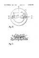
- FIG. 2is a top view of the conventional crystal mounting arrangement depicted in cross section in FIG. 1.
- the X and Z crystallographic reference coordinate axes of crystal 10are clearly shown in FIG. 2.
- crystal 10which exhibits a substantially circular geometry, is provided with a flat portion 11 which is parallel to the Z crystal-lographic axis of crystal 10. It is noted that the X and Z axes exhibit an orthogonal relationship to each other.
- the Y crystallographic axis(not shown) is orthogonal to the X and Z axes.
- the circular raised portion 52 which supports crystal 10is shown as a circular dashed line in the top view of the conventional crystal mounting arrangement shown in FIG. 2.
- crystal mounting arrangement depicted in FIGS. 1 and 2performs well to support crystal 10 and provide electrical connection thereto, it is found that when such crystal mounting arrangement is subjected to changes of temperature, differential thermal expansion results between raised portion 52 on substrate 50 and crystal plate 10. Such differential thermal expansion causes stresses to be generated in crystal plate 10 which tend to result in changes of the resonant frequency of resonators disposed on crystal plate 10 in excess of those normally observed for an AT cut crystal. In some applications, such frequency variation over temperature change may be undesirable.
- the present inventionis directed to providing a piezoelectric crystal mounting arrangement which results in the crystal being relatively insensitive to changes in temperature tending to cause changes in the resonant frequency of resonators disposed on such crystal.
- the piezoelectric crystal mounting arrangementincludes a substrate of electrically insulative material.
- the mounting arrangementfurther includes a piezoelectric crystal plate having opposed upper and lower surfaces. At least one electrode is disposed on the upper surface of the crystal plate, and at lease one electrode is disposed on the lower surface of the crystal plate.
- the crystal plateexhibits X, Y, and Z reference coordinate axes.
- a plurality of pedestalsare situated on the substrate and are oriented so as to contact and support the crystal plate along at least one selected axis thereof which exhibits piezoelectric coefficients substantially insensitive to stress applied to the crystal plate.
- FIG. 1is a cross-sectional representation of a conventional center supported piezoelectric crystal mounting arrangement.
- FIG. 2is a top view of the conventional crystal mounting arrangement of FIG. 1.
- FIG. 3Ais a simplified representation of a top view of the crystal mounting arrangement of the present invention showing a plurality of support pedestals below the crystal.
- FIG. 3Bis a simplified representation of a top view of the crystal mounting arrangement of the present invention.
- FIG. 3Cis a more detailed cross section of the crystal mounting arrangement of FIG. 3A.
- FIG. 4is a simplified representation of a top view of another embodiment of the crystal mounting arrangement of the present invention.
- FIG. 5is a top view of yet another embodiment of the crystal mounting arrangement of the present invention.
- FIG. 3Aillustrates a simplified top view of the crystal mounting arrangement of the present invention.
- Such crystal mounting arrangementincludes a piezoelectric crystal plate 110 exhibiting X, Y, and Z reference coordinate (crystallographic) axes.
- the X and Z crystallographic axes of crystal plate 110 which exhibits an AT cut in this embodiment of the invention,are clearly shown in FIG. 3A.
- the X crystallographic axisis perpendicular to a reference flat 111 which is formed at the edge of crystal 110 in a direction parallel to the Z crystallographic axis.
- crystal 110is shown without any electrode configurations disposed on the upper surface 112 thereof. In actual practice, such electrode configurations take the form of resonator and/or filter metallizations.
- Crystal 110is situated atop a plurality of electrically conductive pedestals 121, 122, 123, and 124 which are situated on a substrate 130 of electrically insulative material as shown in FIG. 3A. It is found that the following axes in the X-Z plane of crystal 110 exhibit piezoelectric coefficients which are substantially insensitive to stresses applied to or generated in crystal 110: an axis 141 situated on crystal 110 at approximately 60° measured clockwise from the X crystallographic axis thereof, an axis 142 situated on crystal 110 at approximately 120° measured clockwise from the X crystallographic axis thereof, an axis 143 situated on crystal 110 at approximately 240° measured clockwise from the X crystallographic axis thereof and axis 144 situated on crystal 110 at approximately 300° measured clockwise from the X crystallographic axis of crystal 110. That is, stresses generated in crystal 110 by differential thermal expansion of substrate 130 and crystal 110 over changes in temperature do not substantially change the piezoelectric coefficients exhibited by axes 141-
- Pedestals 121, 122, 123, and 124are appropriately located on substrate 130 such that when crystal 110 is situated atop such pedestals, pedestals 121, 122, 123, and 124 are aligned with and contact axes 141, 142, 143, and 144, respectively of crystal 110.
- Pedestals 121-124are conveniently secured to the bottom surface of crystal 110 via respective layers of electrically conductive epoxy (not shown in FIG. 3A). Electrical connection between electrodes situated on the bottom surface of crystal 110 and locations on substrate 130 may thus be conveniently achieved.
- the crystal mounting arrangement of FIG. 3Aachieves crystal mounting in a manner which permits crystal 110 to be operated over a relatively wide temperature range without inducing substantial stresses in such crystal 110 due to differential thermal expansion between substrate 130 and crystal 110. This is so because the aforementioned pedestals 121-124 which support crystal 110 are situated on substrate 130 in positions which permit such pedestals to contact crystal 110 on respective axes which exhibit piezoelectric coefficients which remain substantially constant despite stresses induced in crystal 110 by changes in temperature. Thus, the operating frequency or frequencies of crystal 110 are not substantially affected by changes in ambient temperature.
- pedestals 121-124are located near the center 150 of crystal 110, it will be appreciated that such pedestals may alternatively be located closer to the edge of crystal 110 than shown, provided that such pedestals are situated along the aforementioned crystallographic axes 141, 142, 143, and 144.
- substantially circular pedestalsare employed for pedestals 121-124, other cross section geometries such as elliptical, oval, substantially cylindroidal, square, and rectangular, for example, may be employed providing such pedestals are confined to contactng crystal 110 along the aforementioned crystallographic axes 141, 142, 143, and 144.
- FIG. 3Bshows a somewhat more detailed representation of the crystal mounting arrangement of FIG. 3A.
- crystal 110 of FIG. 3Bclearly shows various electrode metallizations on upper surface 112 which are to be electrically connected to various electrically conductive regions situated on substrate 130.
- electrodes 160 and 170are situated on the upper surface 112 of crystal 110. Electrodes 160 and 170 are electrically coupled to the outer peripheral edge 125 of crystal 110 via lead attachment tabs and bonding pads 162 and 172. Lead attachments tabs 162 and 172 are conveniently flared or widened as the edge of the crystal is approached by such respective pads to facilitate wire bonding thereto as discussed subsequently.
- Electrically conductive regions 164 and 174are situated on substrate 130 at loci adjacent the edge 125 of crystal 110 and bonding pads 162 and 172, respectively.
- a flexible wire bond 166has its opposed ends respectively wire-bonded to conductive region 164 and bonding pad 162 in accordance with the teachings of the above-incorporated U.S. Pat. Nos. 4,282,454 and 4,334,343.
- a flexible wire bond 176has its opposed ends wirebonded to bonding pad 172 and conductive region 174, respectively in accordance with the aforementioned patents.
- FIG. 3Cis a cross-section of the crystal mounting arrangement of FIG. 3B taken along cross section line 3C-3C of FIG. 3B.
- FIG. 3Cmore clearly shows the various metallizations on the upper surface 112 and the lower surface 114 of crystal plate 110 as well as the flexible wire bonds 166 and 176 which couple crystal 110 to external electrical circuitry. Analyzing FIG. 3C with respect to FIG. 3B, like numbers indicate like elements. For sake of completeness, however, the entire structure shown in FIG. 3C will now be briefly discussed.
- Electrodes 160 and 170are disposed on upper surface 112 of crystal plate 110. Electrodes 180 and 190 are disposed on lower surface 114 immediately opposite electrodes 160 and 170, respectively. Electrodes 160 and 180 act together to form a resonator 182. Similarly, electrodes 170 and 190 act together to form a resonator 192. As seen in FIG. 3C, pedestals 121 and 124 (as well as pedestals 122 and 123, not shown) are contacted by electrically conductive pedestal receiving pads 201 and 204, respectively. Pedestal receiving pads 201 and 204 are appropriately situated on the lower surface 114 of crystal 110 on axes 144 and 141, respectively in accordance with the previous discussion.
- Electrode 180is electrically coupled to pedestal receiving pad 204 via a runner 186 of electrically conductive material situated therebetween.
- pedestal receiving pad 201is electrically coupled to electrode 190 via a runner 206 of electrically conductive material situated therebetween.
- electrodes 180 and 190are electrically coupled to pedestals 124 and 121, respectively, and external electrical circuitry connected to such pedestals.
- Layers 211 and 214 of electrically conductive epoxyare employed to electrically and mechanically connect pedestal 121 to pedestal receiving pad 201 and to so connect pedestal 124 to pedestal receiving pad 204, respectively.
- Flexible wire bonds 166 and 176have already been fully discussed.
- FIGS. 3B and 3Care given merely by way of example. Virtually any electrode configuration, whether for purposes of filtering or oscillation or otherwise, may be adapted to be situated in the crystal mounting structure exemplified in FIGS. 3B and 3C.
- FIG. 4illustrates a top view of an alternative embodiment of the present crystal mounting arrangement invention.
- An AT cut crystal 310 to be mountedexhibits X, Y, and Z crystallographic axes with a flat 311 being situated in crystal 310 parallel with the Z crystallographic axes.
- the aforementioned substantially dimensionally temperature insensitive axes for an AT cut crystal such as crystal 310are designated 341, 342, 343, and 344.
- Axes 341, 342, 343, and 344are respectively situated at approximately 60°, 120°, 240°, and 300°, with respect to the X crystallographic axes.
- pedestalssuch as those described above under the discussion of FIGS.
- 3A-3Care situated on each of two diametrically opposed axes selected from axes 341, 342, 343 and 344.
- pedestals 321 and 323are situated on diametrically opposed axes 341 and 343.
- pedestals 322 and 323are situated along diametrically opposed axes 342 and 344.
- pedestalsare defined to be diametrically opposed when such pedestals and the intersection of the X-Z crystallographic axes are substantially collinear, and such pedestals are on opposed sides of the intersection of the X-Z axes.
Landscapes
- Physics & Mathematics (AREA)
- Acoustics & Sound (AREA)
- Piezo-Electric Or Mechanical Vibrators, Or Delay Or Filter Circuits (AREA)
Abstract
Description
Claims (16)
Priority Applications (1)
| Application Number | Priority Date | Filing Date | Title |
|---|---|---|---|
| US06/408,409US4430596A (en) | 1982-08-16 | 1982-08-16 | Temperature insensitive piezoelectric crystal mounting arrangement |
Applications Claiming Priority (1)
| Application Number | Priority Date | Filing Date | Title |
|---|---|---|---|
| US06/408,409US4430596A (en) | 1982-08-16 | 1982-08-16 | Temperature insensitive piezoelectric crystal mounting arrangement |
Publications (1)
| Publication Number | Publication Date |
|---|---|
| US4430596Atrue US4430596A (en) | 1984-02-07 |
Family
ID=23616174
Family Applications (1)
| Application Number | Title | Priority Date | Filing Date |
|---|---|---|---|
| US06/408,409Expired - LifetimeUS4430596A (en) | 1982-08-16 | 1982-08-16 | Temperature insensitive piezoelectric crystal mounting arrangement |
Country Status (1)
| Country | Link |
|---|---|
| US (1) | US4430596A (en) |
Cited By (11)
| Publication number | Priority date | Publication date | Assignee | Title |
|---|---|---|---|---|
| US4533885A (en)* | 1983-04-27 | 1985-08-06 | Motorola, Inc. | Apparatus for suppression of spurious attenuation poles in crystal filters |
| EP0293591A3 (en)* | 1987-05-01 | 1989-02-01 | Abbott Laboratories | Ultrasonic detector |
| US4802371A (en)* | 1986-11-07 | 1989-02-07 | Kristal Instrumente Ag | Multi-component dynamometers |
| US4825117A (en)* | 1987-11-27 | 1989-04-25 | General Electric Company | Temperature compensated piezoelectric transducer assembly |
| US4921415A (en)* | 1987-11-27 | 1990-05-01 | General Electric Company | Cure monitoring apparatus having high temperature ultrasonic transducers |
| US4967165A (en)* | 1989-02-14 | 1990-10-30 | Motorola, Inc. | Crystal reference for use in oscillator circuit |
| US5041799A (en)* | 1990-11-05 | 1991-08-20 | Motorola, Inc. | Temperature compensation circuit for a crystal oscillator |
| AU627094B2 (en)* | 1987-05-01 | 1992-08-13 | Abbott Laboratories | Ultrasonic detector |
| US5185550A (en)* | 1990-02-09 | 1993-02-09 | Toyo Communication Equipment Co., Ltd. | Structure for supporting a resonator using an ultrathin piezoelectric plate in a package |
| US20040000844A1 (en)* | 2002-06-28 | 2004-01-01 | Morley Peter E. | Low profile temperature-compensated low-stress crystal mount structure |
| US20040021402A1 (en)* | 2002-05-28 | 2004-02-05 | Morley Peter E. | Low acceleration sensitivity mounting structures for crystal resonators |
Citations (12)
| Publication number | Priority date | Publication date | Assignee | Title |
|---|---|---|---|---|
| US2284284A (en) | 1939-06-24 | 1942-05-26 | Us Rubber Co | Treatment of rubber |
| US2410825A (en) | 1943-03-04 | 1946-11-12 | Bell Telephone Labor Inc | Piezoelectric crystal apparatus |
| US2639393A (en) | 1948-02-26 | 1953-05-19 | Piezo Crystals Ltd | Mounting and holder for piezoelectric crystals |
| US2771561A (en) | 1952-03-17 | 1956-11-20 | Pye Ltd | Quartz crystal units |
| US3069572A (en) | 1958-12-02 | 1962-12-18 | James Knights Company | Piezoelectric device |
| US3073975A (en) | 1958-12-23 | 1963-01-15 | Rca Corp | Crystal unit |
| US3527967A (en) | 1968-06-04 | 1970-09-08 | Gen Electric & English Electri | Monolithic crystal filters with ultrasonically lossy mounting means |
| US4112323A (en) | 1976-01-29 | 1978-09-05 | Kabushiki Kaisha Daini Seikosha | Circular flexural mode piezoelectric vibrator with integral support arms |
| US4266157A (en) | 1979-05-18 | 1981-05-05 | The United States Of America As Represented By The Secretary Of The Army | Piezoelectric resonator assembly with thin molybdenum mounting clips |
| US4282454A (en) | 1979-04-27 | 1981-08-04 | Motorola, Inc. | Piezoelectric crystal mounting and connection arrangement |
| US4292562A (en) | 1979-05-03 | 1981-09-29 | Motorola, Inc. | Mounting arrangement for crystal assembly |
| US4357554A (en) | 1980-05-21 | 1982-11-02 | The United States Of America As Represented By The Secretary Of The Army | Hexagonal quartz resonator |
- 1982
- 1982-08-16USUS06/408,409patent/US4430596A/ennot_activeExpired - Lifetime
Patent Citations (12)
| Publication number | Priority date | Publication date | Assignee | Title |
|---|---|---|---|---|
| US2284284A (en) | 1939-06-24 | 1942-05-26 | Us Rubber Co | Treatment of rubber |
| US2410825A (en) | 1943-03-04 | 1946-11-12 | Bell Telephone Labor Inc | Piezoelectric crystal apparatus |
| US2639393A (en) | 1948-02-26 | 1953-05-19 | Piezo Crystals Ltd | Mounting and holder for piezoelectric crystals |
| US2771561A (en) | 1952-03-17 | 1956-11-20 | Pye Ltd | Quartz crystal units |
| US3069572A (en) | 1958-12-02 | 1962-12-18 | James Knights Company | Piezoelectric device |
| US3073975A (en) | 1958-12-23 | 1963-01-15 | Rca Corp | Crystal unit |
| US3527967A (en) | 1968-06-04 | 1970-09-08 | Gen Electric & English Electri | Monolithic crystal filters with ultrasonically lossy mounting means |
| US4112323A (en) | 1976-01-29 | 1978-09-05 | Kabushiki Kaisha Daini Seikosha | Circular flexural mode piezoelectric vibrator with integral support arms |
| US4282454A (en) | 1979-04-27 | 1981-08-04 | Motorola, Inc. | Piezoelectric crystal mounting and connection arrangement |
| US4292562A (en) | 1979-05-03 | 1981-09-29 | Motorola, Inc. | Mounting arrangement for crystal assembly |
| US4266157A (en) | 1979-05-18 | 1981-05-05 | The United States Of America As Represented By The Secretary Of The Army | Piezoelectric resonator assembly with thin molybdenum mounting clips |
| US4357554A (en) | 1980-05-21 | 1982-11-02 | The United States Of America As Represented By The Secretary Of The Army | Hexagonal quartz resonator |
Non-Patent Citations (3)
| Title |
|---|
| "Effect of Internal Stress in Vibrating Quartz Plates" Ballato, A. D., and Bechman, R., Proc. IRE 48 (1960). |
| "Stress Induced Frequency Shifts in Thickness Mode Quartz Resonators." Sinha, B. K., Proc of the 1980 IEEE Ultrasonic Symposium. |
| "The Force Sensitivity of AT Cut Quartz Crystals", Ratajski, Proc. 20th Annual Frequency Control Symposium (1966). |
Cited By (13)
| Publication number | Priority date | Publication date | Assignee | Title |
|---|---|---|---|---|
| US4533885A (en)* | 1983-04-27 | 1985-08-06 | Motorola, Inc. | Apparatus for suppression of spurious attenuation poles in crystal filters |
| US4802371A (en)* | 1986-11-07 | 1989-02-07 | Kristal Instrumente Ag | Multi-component dynamometers |
| AU607213B2 (en)* | 1987-05-01 | 1991-02-28 | Abbott Laboratories | Ultrasonic detector |
| EP0293591A3 (en)* | 1987-05-01 | 1989-02-01 | Abbott Laboratories | Ultrasonic detector |
| AU627094B2 (en)* | 1987-05-01 | 1992-08-13 | Abbott Laboratories | Ultrasonic detector |
| US4825117A (en)* | 1987-11-27 | 1989-04-25 | General Electric Company | Temperature compensated piezoelectric transducer assembly |
| US4921415A (en)* | 1987-11-27 | 1990-05-01 | General Electric Company | Cure monitoring apparatus having high temperature ultrasonic transducers |
| US4967165A (en)* | 1989-02-14 | 1990-10-30 | Motorola, Inc. | Crystal reference for use in oscillator circuit |
| US5185550A (en)* | 1990-02-09 | 1993-02-09 | Toyo Communication Equipment Co., Ltd. | Structure for supporting a resonator using an ultrathin piezoelectric plate in a package |
| US5041799A (en)* | 1990-11-05 | 1991-08-20 | Motorola, Inc. | Temperature compensation circuit for a crystal oscillator |
| US20040021402A1 (en)* | 2002-05-28 | 2004-02-05 | Morley Peter E. | Low acceleration sensitivity mounting structures for crystal resonators |
| US6984925B2 (en) | 2002-05-28 | 2006-01-10 | Delaware Capital Formation, Inc | Low acceleration sensitivity mounting structures for crystal resonators |
| US20040000844A1 (en)* | 2002-06-28 | 2004-01-01 | Morley Peter E. | Low profile temperature-compensated low-stress crystal mount structure |
Similar Documents
| Publication | Publication Date | Title |
|---|---|---|
| US4430596A (en) | Temperature insensitive piezoelectric crystal mounting arrangement | |
| US5235240A (en) | Electrodes and their lead structures of an ultrathin piezoelectric resonator | |
| US6369487B1 (en) | Piezoelectric resonance component | |
| EP0644653A2 (en) | Packaged piezoelectric resonator | |
| EP1653613B1 (en) | Saw filter encapsulated in a ceramic package with capacitance incorporated therein | |
| US4639632A (en) | Piezoelectric resonator mountings | |
| JPH07112142B2 (en) | Piezoelectric resonator sealing structure | |
| US6236140B1 (en) | Piezoelectric vibration device | |
| US5218328A (en) | Structure for a resonator using an ultrathin piezoelectric substrate | |
| US6563400B2 (en) | Piezoelectric resonator utilizing bending vibrations and ladder-type filter including the same | |
| JPH07321140A (en) | Semiconductor device | |
| US6333591B1 (en) | Piezoelectric resonator | |
| US20020180307A1 (en) | Surface acoustic wave device and communication apparatus including the same | |
| US4340901A (en) | Lead connecting structure for a semiconductor device | |
| JPH0422566Y2 (en) | ||
| CN113243081B (en) | Crystal Oscillator Devices | |
| JPH0435107A (en) | Electrode lead structure of multiple mode filter element using ultra thin piezoelectric resonator | |
| JP3259832B2 (en) | Surface acoustic wave device | |
| US20020030564A1 (en) | Die layout for SAW devices and associated methods | |
| JPS6340909Y2 (en) | ||
| JPS5927059Y2 (en) | Hybrid integrated circuit device | |
| JPH036029Y2 (en) | ||
| JPH0388373A (en) | Surface-mounted piezoelectric vibrator | |
| JPH0583083A (en) | Piezoelectric component | |
| JPH0435106A (en) | Electrode lead connection structure of ultra thin piezoelectric resonator |
Legal Events
| Date | Code | Title | Description |
|---|---|---|---|
| AS | Assignment | Owner name:MOTOROLA, INC., SCHAUMBURG, ILL., A CORP. OF DEL. Free format text:ASSIGNMENT OF ASSIGNORS INTEREST.;ASSIGNOR:SHANLEY, CHARLES W.;REEL/FRAME:004084/0856 Effective date:19820810 | |
| STCF | Information on status: patent grant | Free format text:PATENTED CASE | |
| MAFP | Maintenance fee payment | Free format text:PAYMENT OF MAINTENANCE FEE, 4TH YEAR, PL 96-517 (ORIGINAL EVENT CODE: M170); ENTITY STATUS OF PATENT OWNER: LARGE ENTITY Year of fee payment:4 | |
| MAFP | Maintenance fee payment | Free format text:PAYMENT OF MAINTENANCE FEE, 8TH YEAR, PL 96-517 (ORIGINAL EVENT CODE: M171); ENTITY STATUS OF PATENT OWNER: LARGE ENTITY Year of fee payment:8 | |
| MAFP | Maintenance fee payment | Free format text:PAYMENT OF MAINTENANCE FEE, 12TH YEAR, LARGE ENTITY (ORIGINAL EVENT CODE: M185); ENTITY STATUS OF PATENT OWNER: LARGE ENTITY Year of fee payment:12 | |
| FEPP | Fee payment procedure | Free format text:PAYOR NUMBER ASSIGNED (ORIGINAL EVENT CODE: ASPN); ENTITY STATUS OF PATENT OWNER: LARGE ENTITY | |
| AS | Assignment | Owner name:CTS CORPORATION, INDIANA Free format text:ASSIGNMENT OF ASSIGNORS INTEREST;ASSIGNOR:MOTOROLA, INC., A CORPORATION OF DELAWARE;REEL/FRAME:009808/0378 Effective date:19990226 | |
| FEPP | Fee payment procedure | Free format text:PAYOR NUMBER ASSIGNED (ORIGINAL EVENT CODE: ASPN); ENTITY STATUS OF PATENT OWNER: LARGE ENTITY Free format text:PAYER NUMBER DE-ASSIGNED (ORIGINAL EVENT CODE: RMPN); ENTITY STATUS OF PATENT OWNER: LARGE ENTITY |