US4417784A - Multiple image encoding using surface relief structures as authenticating device for sheet-material authenticated item - Google Patents
Multiple image encoding using surface relief structures as authenticating device for sheet-material authenticated itemDownload PDFInfo
- Publication number
- US4417784A US4417784AUS06/236,111US23611181AUS4417784AUS 4417784 AUS4417784 AUS 4417784AUS 23611181 AUS23611181 AUS 23611181AUS 4417784 AUS4417784 AUS 4417784A
- Authority
- US
- United States
- Prior art keywords
- given
- comprised
- article defined
- period
- elements
- Prior art date
- Legal status (The legal status is an assumption and is not a legal conclusion. Google has not performed a legal analysis and makes no representation as to the accuracy of the status listed.)
- Expired - Fee Related
Links
Images

Classifications
- G—PHYSICS
- G02—OPTICS
- G02B—OPTICAL ELEMENTS, SYSTEMS OR APPARATUS
- G02B3/00—Simple or compound lenses
- G02B3/0006—Arrays
- G02B3/0037—Arrays characterized by the distribution or form of lenses
- G02B3/005—Arrays characterized by the distribution or form of lenses arranged along a single direction only, e.g. lenticular sheets
- G—PHYSICS
- G06—COMPUTING OR CALCULATING; COUNTING
- G06K—GRAPHICAL DATA READING; PRESENTATION OF DATA; RECORD CARRIERS; HANDLING RECORD CARRIERS
- G06K19/00—Record carriers for use with machines and with at least a part designed to carry digital markings
- G06K19/06—Record carriers for use with machines and with at least a part designed to carry digital markings characterised by the kind of the digital marking, e.g. shape, nature, code
- G06K19/08—Record carriers for use with machines and with at least a part designed to carry digital markings characterised by the kind of the digital marking, e.g. shape, nature, code using markings of different kinds or more than one marking of the same kind in the same record carrier, e.g. one marking being sensed by optical and the other by magnetic means
- G06K19/10—Record carriers for use with machines and with at least a part designed to carry digital markings characterised by the kind of the digital marking, e.g. shape, nature, code using markings of different kinds or more than one marking of the same kind in the same record carrier, e.g. one marking being sensed by optical and the other by magnetic means at least one kind of marking being used for authentication, e.g. of credit or identity cards
- G06K19/16—Record carriers for use with machines and with at least a part designed to carry digital markings characterised by the kind of the digital marking, e.g. shape, nature, code using markings of different kinds or more than one marking of the same kind in the same record carrier, e.g. one marking being sensed by optical and the other by magnetic means at least one kind of marking being used for authentication, e.g. of credit or identity cards the marking being a hologram or diffraction grating
- G—PHYSICS
- G07—CHECKING-DEVICES
- G07F—COIN-FREED OR LIKE APPARATUS
- G07F7/00—Mechanisms actuated by objects other than coins to free or to actuate vending, hiring, coin or paper currency dispensing or refunding apparatus
- G07F7/08—Mechanisms actuated by objects other than coins to free or to actuate vending, hiring, coin or paper currency dispensing or refunding apparatus by coded identity card or credit card or other personal identification means
- G07F7/086—Mechanisms actuated by objects other than coins to free or to actuate vending, hiring, coin or paper currency dispensing or refunding apparatus by coded identity card or credit card or other personal identification means by passive credit-cards adapted therefor, e.g. constructive particularities to avoid counterfeiting, e.g. by inclusion of a physical or chemical security-layer
- G—PHYSICS
- G09—EDUCATION; CRYPTOGRAPHY; DISPLAY; ADVERTISING; SEALS
- G09F—DISPLAYING; ADVERTISING; SIGNS; LABELS OR NAME-PLATES; SEALS
- G09F3/00—Labels, tag tickets, or similar identification or indication means; Seals; Postage or like stamps
- G—PHYSICS
- G02—OPTICS
- G02B—OPTICAL ELEMENTS, SYSTEMS OR APPARATUS
- G02B3/00—Simple or compound lenses
- G02B3/0006—Arrays
- G02B3/0012—Arrays characterised by the manufacturing method
- G02B3/0031—Replication or moulding, e.g. hot embossing, UV-casting, injection moulding
- Y—GENERAL TAGGING OF NEW TECHNOLOGICAL DEVELOPMENTS; GENERAL TAGGING OF CROSS-SECTIONAL TECHNOLOGIES SPANNING OVER SEVERAL SECTIONS OF THE IPC; TECHNICAL SUBJECTS COVERED BY FORMER USPC CROSS-REFERENCE ART COLLECTIONS [XRACs] AND DIGESTS
- Y10—TECHNICAL SUBJECTS COVERED BY FORMER USPC
- Y10S—TECHNICAL SUBJECTS COVERED BY FORMER USPC CROSS-REFERENCE ART COLLECTIONS [XRACs] AND DIGESTS
- Y10S428/00—Stock material or miscellaneous articles
- Y10S428/916—Fraud or tamper detecting
Definitions
- This inventionrelates to devices for authenticating various items of sheet materials which are subject to counterfeiting, such as bank notes and other valuable documents, credit cards, passports, security passes, and phonograph records or their covers, for example.
- the present inventionis related to the respective invention disclosed in U.S. patent application Ser. No. 235,970 by Webster, et al, filed on even date herewith and assigned to the same assignee as the present application.
- any authenticating device for solving this problemmust, inter alia, meet all four of the following criteria:
- the authenticating devicemust produce an effect which is not capable of being reproduced by any type of color copier.
- the effect produced by the authenticating devicemust be quickly and readily discernable, under ordinary lighting conditions, without requiring any significant degree of skill on the part of an unsophisticated layman.
- the present inventionis directed to authenticating device which meets all of the above set forth for criteria. More specifically, the present invention is similar to that disclosed in aforesaid U.S. patent application Ser. No. 235,970 to the extent that both cases a substrate is bonded to sheet material of which an authenticating item subject to counterfeiting is comprised. This substrate has a reflective periodic structure formed as a relief pattern on a viewable surface thereof. Further, in both cases, a transparent material fills and covers the structure, the transparent material exhibiting a given index-of-refraction and being bonded to the viewable surface of the substrate in a manner sufficiently secure to prevent the transparent material from being removed from the structure without effectively destroying the structure.
- the reflective periodic structure formed as a relief pattern on a viewable surface of the substrate of the authenticated deviceis limited to a reflective diffraction grating structure.
- the periodic structuremay take any form in which the period thereof is smaller than 100 micrometers and each period is comprised of substantially the same given set of a plural number of juxtaposed elements, respective elements of the given set having significantly different characteristics from one another.
- a transparent materialhas a given thickness of no greater than 100 micrometers and has a periodic lenticular array embossed on that surface thereof which is situated distal to the periodic structure.
- Each period of the arrayis comprised of a lens having an aperture width that at least approximates that of a period of the structure and has a focal length substantially equal to the given thickness of the transparent material.
- FIG. 1is a schematic diagram of a first embodiment of authenticated item having an authenticated device, comprised of a single integrated structure, bonded thereto;
- FIG. 1ais a schematic diagram of a second embodiment of an authenticated item having an authenticating device, comprised of a plurality of spaced integrated structures bonded thereto;
- FIG. 2is a schematic diagram of a prior art structure which is similar in certain respects to that of an integrated structure of the authenticating device in the present invention
- FIG. 3is a schematic diagram of a first embodiment of an integrated structure of the present invention.
- FIG. 4is a schematic diagram of a second embodiment of an integrated structure of the present invention.
- FIG. 5is a schematic diagram of a third embodiment of an integrated structure of the present invention.
- authenticated item 100comprised of a sheet material, such as plastic or paper.
- authenticated item 100is a bank note.
- authenticated item 100may take other forms, such as other types of valuable documents having intrinsic value, credit cards passports, security passes, or phonograph records or covers therefor, by way of examples.
- authenticated item 100has bonded thereto authenticating device 102.
- Authenticating device 102consists of a single integrated structure.
- authenticating device 102aconsists of a plurality of two (or more) spaced integrated structures.
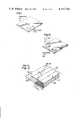
- FIG. 2there is shown a prior art technique for storing multiple images in a single plane 200.
- a lenticular array 202consisting of multiple cylindrical lenses 204 is placed at the focal distance f in front of plane 200 containing the image information A, B, C and D.
- the lenslets 204are formed as a relief structure on one side of a plastic sheet 206, and the image information A, B, C and D is printed on the other side by conventional printing techniques.
- each individual pictureis separately read out by viewing at a different appropriate angle.
- lenslets 204are oriented on a vertical axis such that the left eye and the right eye see different pictures and thus, produce an illusion of depth.
- lenslets 204in this application, have a width l of about 0.3-0.4 mm and a focal distance f of similar size.
- image multiplexing by lenticular arraysis employed in an authenticating device for an authenticated item comprised of a sheet material.
- the prior art arrangement shown in FIG. 2cannot be used for this purpose. This is because the thickness of sheet material (such as bank note paper) is typically around 0.1 mm, and the authenticating device should not add significantly to the thickness of this sheet material. Therefore, the thickness f (the focal length of lenslets 204 of lenticular array 202 and the respective widths l of lenslets 204 can never be as large in size as 0.1 mm. Preferably, f and l could be in range of 0.01-0.05 mm. Stripes of such dimensions are smaller than can be produced with today's best printing techniques.
- Sheet 300like sheet 206 of the prior art arrangement shown in FIG. 2, has a lenticular array, composed of lenslets 302, embossed on the upper surface thereof.
- the thickness f of sheet 300 and the width l of lenslets 302are each smaller in size than 100 micrometers, preferably being in the range of between 10 and 50 micrometers.
- the relief patternis oriented substantially parallel to the lenticular array. More particularly, in the first embodiment of the present invention, shown in FIG. 3, the relief pattern 304 comprises periodically arranged sets of different diffraction grating structures. Each period of relief structure 304 is l widths, which, alternatively, may be identical to slightly different from the size of l.
- the different diffractive structures forming the juxtaposed elements of the set associated with each periodmay constitute reflective sinusoidal grating structures (such as grating structure A of FIG. 3), reflective rectangular-wave grating structures (such as grating structure B of FIG. 3), or a reflective grating structure of any other desired grating profile, or a mixture of different grating profiles.
- the grating profile, line spacing and/or amplitude of the different reflective grating structures forming the same given set for respective ones of the periods of relief patterns 304are selected so that they reflect incident polychromatic light with appreciably different chrominance and/or luminance effects.
- Relief pattern 304as well as lenticular lenses 302, can be easily and inexpensively fabricated by simultaneously embossing sheet 300 on both sides with appropriate platens in a suitable press. Thereafter, relief structure 304 may be made reflective by vacuum deposition (evaporation or sputtering) of a reflective metal coating. After fabrication, sheet 300 may be attached as an integrated structure of the authenticating device to authenticated item 100 by a layer of adhesive 306, which bonds the undersurface of relief pattern 304 to a surface of authenticated item 100.
- Corresponding elements (such as element A in FIG. 3) of respective periods of relief pattern 304may be substantially identical in all respects so that as the eye angularly moves, stripes of different color and/or contrast are seen.
- corresponding elements (such as element A in FIG. 3) of respective periods of relief pattern 304may be spatially modulated (e.g., such as amplitude) in accordance with picture information on a large scale.
- the width of l 1 of a period of relief pattern 304is substantially equal to the width l of a lenticular lens 302, there will be a switching effect as the eye is angularly moved between the multiple images defined by respective specified ones of juxtaposed elements (such as elements A or elements B).
- the respective position of the multiple imagesappears to move continuously as the viewing angle changes.
- the sinusoidal and rectangular-wave profile diffraction grating structuresare specifically shown in FIG. 3 because they have well-defined reflection characteristics that make them suitable for use in the present invention.
- grating structures having other profilescan also be employed.
- the grating structuresmay be oriented at an angle different from zero (with respect to lenslets 302).
- the juxtaposed elements of the reflective periodic relief pattern structureneed not be composed of diffraction grating structures, as shown in FIG. 3.
- the juxtaposed elements of each period of the reflective periodic structure formed by relief pattern 404may be comprised of plane mirror reflectors (e.g., juxtaposed elements A, B and C), each having a different slope from one another with respect to the plane of the lenticular array formed by lenslets 402. Differences in the reflection characteristics of elements A, B and C of pattern 404, with respect to one another, can be enhanced further by coating the separate elements A, B and C differently. For instance, evaporating various materials at different angles produces respective mirrors for juxtaposed elements A, B and C which exhibit inherently different reflectivities.
- Respective items 400, 402 and 406 of the embodiment of the present invention shown in FIG. 4are identical in structure and function to the corresponding items 300, 302 and 306 of the first embodiment of the present invention shown in FIG. 3.
- FIG. 5A third embodiment of the present invention is shown in FIG. 5.
- juxtaposed elements A, B and C of each period of a reflective periodic structure formed by relief pattern 504exhibit different textures from one another.
- elements A and C of relief pattern 504represent two types of random relief patterns which are originally produced in a pressing master by different methods, (e.g., sandblasting, chemical etching or exposure of a photoresist with a diffuse light, for example) which result in distinguishable reflective textures.
- Element B of relief pattern 504is a plane mirror, which inherently has a higher reflectivity and a different texture from either element A or element C.
- Respective items 500, 502 and 506 of the third embodiment shown in FIG. 5are identical in structure and function to the corresponding items 300, 302 and 306 of the first embodiment shown in FIG. 3.
- each periodis comprised of substantially the same given set of a plural number of juxtaposed elements, respective elements of the given set having significantly different reflective characteristics from one another.
- a lenticular array with a period of 15 micrometers and a focal length of 40 micrometerswas embossed on one side of the sheet of polyvinylchloride (PVC) having a thickness of 40 micrometers.
- a relief pattern structure, which conformed to the second embodiment of the present invention shown in FIG. 4,consisted of three plane segments of about equal length and with the slope of 0°, -55° and +55° (V groove and plane surface). Both the lenticular array and the relief structure were hot embossed into the 40 micrometer thick VC sheet. Then the relief pattern structure was coated with a thin layer of gold and subsequently with a thicker layer of aluminum by evaporation techniques. Finally, the plastic sheet was glued onto paper.
- the narrowest dimension of the size of the respective light-formed images and of the dual-formed imageswas sufficient to subtend an angle substantially larger than two milliradians at a viewing distance of 30 centimeters. This size was more than sufficient to permit an unsophisticated layman to quickly and readily discern the respective images under ordinary lighting conditions (i.e., comply with criterion 2 above). Furthermore, the widths of the respective lenslets and relief pattern periods were slightly different from each other, so that the multiple images appeared to move when viewed at different angles. This effect in the experimental device is not capable of being reproduced by any type of copier (i.e., comply with criterion 1 above).
Landscapes
- Physics & Mathematics (AREA)
- General Physics & Mathematics (AREA)
- Engineering & Computer Science (AREA)
- Theoretical Computer Science (AREA)
- Optics & Photonics (AREA)
- Computer Security & Cryptography (AREA)
- Credit Cards Or The Like (AREA)
Abstract
Description
This invention relates to devices for authenticating various items of sheet materials which are subject to counterfeiting, such as bank notes and other valuable documents, credit cards, passports, security passes, and phonograph records or their covers, for example. The present invention is related to the respective invention disclosed in U.S. patent application Ser. No. 235,970 by Webster, et al, filed on even date herewith and assigned to the same assignee as the present application.
Recently, there have been great advances in color copying of documents. It is believed that these advances will continue. Therefore, in the near future, it is likely that it will be possible to make a color photocopy of a bank note that the man-in-the-street is incapable of (or, at least, will have great difficulty in) distinguishing from the original. More particularly, while it is true that a genuine bank note makes use of authenticating means (such as inks of many colors and intricate engraved designs on special paper which sometimes contain watermarks or embedded colored platelets or metal threads) which currently permit an expert to distinguish a counterfeit from a genuine bank note, the unsophisticated layman is in no position to make use of such authenticating means. Therefore, as color copying improves, a real danger exists that the man-in-the-street will lose faith in the genuineness of paper currency. Such a situation would create havoc.
In order to be practical, any authenticating device for solving this problem must, inter alia, meet all four of the following criteria:
1. The authenticating device must produce an effect which is not capable of being reproduced by any type of color copier.
2. The effect produced by the authenticating device must be quickly and readily discernable, under ordinary lighting conditions, without requiring any significant degree of skill on the part of an unsophisticated layman.
3. The sophistication and capital cost of the equipment required to fabricate an authenticating device and to securely attach the authenticating device to an authenticated item (e.g., bank note, etc.) must be high enough to be beyond the reach of would-be counterfeiters.
4. Under high volume conditions, the additional per-unit cost of fabricating an authenticating device and securely attaching it to the authenticated item (including both the amortization of the high capital cost of the equipment, as well as the per-unit variable cost) must be low enough not to constitute an impediment to its use.
The present invention is directed to authenticating device which meets all of the above set forth for criteria. More specifically, the present invention is similar to that disclosed in aforesaid U.S. patent application Ser. No. 235,970 to the extent that both cases a substrate is bonded to sheet material of which an authenticating item subject to counterfeiting is comprised. This substrate has a reflective periodic structure formed as a relief pattern on a viewable surface thereof. Further, in both cases, a transparent material fills and covers the structure, the transparent material exhibiting a given index-of-refraction and being bonded to the viewable surface of the substrate in a manner sufficiently secure to prevent the transparent material from being removed from the structure without effectively destroying the structure.
In U.S. patent application Ser. No. 235,970, the reflective periodic structure formed as a relief pattern on a viewable surface of the substrate of the authenticated device is limited to a reflective diffraction grating structure. In the present invention, on the other hand, the periodic structure may take any form in which the period thereof is smaller than 100 micrometers and each period is comprised of substantially the same given set of a plural number of juxtaposed elements, respective elements of the given set having significantly different characteristics from one another. Further, in the present invention, a transparent material has a given thickness of no greater than 100 micrometers and has a periodic lenticular array embossed on that surface thereof which is situated distal to the periodic structure. Each period of the array is comprised of a lens having an aperture width that at least approximates that of a period of the structure and has a focal length substantially equal to the given thickness of the transparent material.
In the drawings:
FIG. 1 is a schematic diagram of a first embodiment of authenticated item having an authenticated device, comprised of a single integrated structure, bonded thereto;
FIG. 1a is a schematic diagram of a second embodiment of an authenticated item having an authenticating device, comprised of a plurality of spaced integrated structures bonded thereto;
FIG. 2 is a schematic diagram of a prior art structure which is similar in certain respects to that of an integrated structure of the authenticating device in the present invention;
FIG. 3 is a schematic diagram of a first embodiment of an integrated structure of the present invention;
FIG. 4 is a schematic diagram of a second embodiment of an integrated structure of the present invention, and
FIG. 5 is a schematic diagram of a third embodiment of an integrated structure of the present invention.
Referring to FIG. 1, there is shownauthenticated item 100 comprised of a sheet material, such as plastic or paper. In describing the present invention, for illustrative purposes, it may be assumed thatauthenticated item 100 is a bank note. However, it should be understood thatauthenticated item 100 may take other forms, such as other types of valuable documents having intrinsic value, credit cards passports, security passes, or phonograph records or covers therefor, by way of examples. In any case,authenticated item 100 has bonded theretoauthenticating device 102.Authenticating device 102 consists of a single integrated structure. In FIG. 1a, authenticating device 102a consists of a plurality of two (or more) spaced integrated structures.
Referring to FIG. 2, there is shown a prior art technique for storing multiple images in asingle plane 200. Alenticular array 202 consisting of multiplecylindrical lenses 204 is placed at the focal distance f in front ofplane 200 containing the image information A, B, C and D. Usually, thelenslets 204 are formed as a relief structure on one side of aplastic sheet 206, and the image information A, B, C and D is printed on the other side by conventional printing techniques. When viewing at a well defined angular direction α with respect to the normal, only a very narrow stripe in the image plane can be seen (i.e., only light from this narrow stripe is reaching theeye 208 of an observer). By dividing the area under eachlenslet 204 into a corresponding set of stripes A, B, C and D, in which the A stripes of corresponding sets contain a first picture, the B stripes of corresponding sets contain a second picture, etc., each individual picture is separately read out by viewing at a different appropriate angle.
The main use of the technique shown in FIG. 2 is for producing serial graphic reproductions in the form of three-dimensional postcards. In this case,cylindrical lenslets 204 are oriented on a vertical axis such that the left eye and the right eye see different pictures and thus, produce an illusion of depth. Typically,lenslets 204, in this application, have a width l of about 0.3-0.4 mm and a focal distance f of similar size.
An earlier application of lenticular arrays for image multiplexing was for the old Kodacolor process. In this case, the three pictures which contain the red, green and blue content of the color picture were recorded in three sets of stripes in a black-and-white photographic emulsion. Due to the high resolution capabilities of the photographic recording, it was possible to use fine lenslets with widths of about 0.05 mm. For recording and readout, three adjacent color filters positioned near the camera/projection lens were needed in the optical path.
In accordance with the principles of the present invention, image multiplexing by lenticular arrays is employed in an authenticating device for an authenticated item comprised of a sheet material. However, the prior art arrangement shown in FIG. 2 cannot be used for this purpose. This is because the thickness of sheet material (such as bank note paper) is typically around 0.1 mm, and the authenticating device should not add significantly to the thickness of this sheet material. Therefore, the thickness f (the focal length oflenslets 204 oflenticular array 202 and the respective widths l oflenslets 204 can never be as large in size as 0.1 mm. Preferably, f and l could be in range of 0.01-0.05 mm. Stripes of such dimensions are smaller than can be produced with today's best printing techniques. In addition, a serious problem in registration is encountered, since the stripes have to be aligned precisely with respect to thelenslets 204 oflenticular array 202 with tolerances of only a few micrometers. Thus, the prior art arrangements of printed stripes A, B, C and D, shown in FIG. 2, cannot be used in implementing the authenticating device of the present invention.
Referring to FIG. 3, there is shown a sheet oftransparent material 300, such as plastic, having a given index-of-refraction.Sheet 300, likesheet 206 of the prior art arrangement shown in FIG. 2, has a lenticular array, composed oflenslets 302, embossed on the upper surface thereof. The thickness f ofsheet 300 and the width l oflenslets 302 are each smaller in size than 100 micrometers, preferably being in the range of between 10 and 50 micrometers. The stripes printed on theplane surface 200 of the prior art arrangement of FIG. 2 are replaced in the present invention, with a reflective periodic structure formed as a relief pattern on a viewable surface of transparent material, in which the period of this periodic structure is smaller in size than 100 micrometers and each period is comprised of substantially the same given set of a plural number of juxtaposed elements, respective elements of the given set having significantly different reflective characteristics from one another. The relief pattern is oriented substantially parallel to the lenticular array. More particularly, in the first embodiment of the present invention, shown in FIG. 3, the relief pattern 304 comprises periodically arranged sets of different diffraction grating structures. Each period of relief structure 304 is l widths, which, alternatively, may be identical to slightly different from the size of l. The different diffractive structures forming the juxtaposed elements of the set associated with each period may constitute reflective sinusoidal grating structures (such as grating structure A of FIG. 3), reflective rectangular-wave grating structures (such as grating structure B of FIG. 3), or a reflective grating structure of any other desired grating profile, or a mixture of different grating profiles. In any event, the grating profile, line spacing and/or amplitude of the different reflective grating structures forming the same given set for respective ones of the periods of relief patterns 304 are selected so that they reflect incident polychromatic light with appreciably different chrominance and/or luminance effects. In this regard, reference is made to the teachings of U.S. Pat. No. 3,957,354, which issued to Knop on May 18, 1976. Also of interest are the teachings of U.S. Pat. No. 4,062,628 which issued to Gale on Dec. 13, 1977 and U.S. Pat. No. 4,130,347 which issued to Knop on Dec. 19, 1978.
Relief pattern 304, as well aslenticular lenses 302, can be easily and inexpensively fabricated by simultaneously embossingsheet 300 on both sides with appropriate platens in a suitable press. Thereafter, relief structure 304 may be made reflective by vacuum deposition (evaporation or sputtering) of a reflective metal coating. After fabrication,sheet 300 may be attached as an integrated structure of the authenticating device to authenticateditem 100 by a layer ofadhesive 306, which bonds the undersurface of relief pattern 304 to a surface of authenticateditem 100.
Corresponding elements (such as element A in FIG. 3) of respective periods of relief pattern 304 may be substantially identical in all respects so that as the eye angularly moves, stripes of different color and/or contrast are seen. Alternatively, corresponding elements (such as element A in FIG. 3) of respective periods of relief pattern 304 may be spatially modulated (e.g., such as amplitude) in accordance with picture information on a large scale. Further, if the width of l1 of a period of relief pattern 304 is substantially equal to the width l of alenticular lens 302, there will be a switching effect as the eye is angularly moved between the multiple images defined by respective specified ones of juxtaposed elements (such as elements A or elements B). Alternatively, by making the size l1 of a period of relief pattern 304 slightly different from (i.e., only approximately equal to) that of the width l of alenticular lens 302, the respective position of the multiple images appears to move continuously as the viewing angle changes.
The sinusoidal and rectangular-wave profile diffraction grating structures are specifically shown in FIG. 3 because they have well-defined reflection characteristics that make them suitable for use in the present invention. However, as discussed above, grating structures having other profiles, (such as triangular, sawtooth and/or lenticular, etc.) can also be employed. Further, in order to enhance differences in reflectivity, the grating structures may be oriented at an angle different from zero (with respect to lenslets 302).
Further, the juxtaposed elements of the reflective periodic relief pattern structure need not be composed of diffraction grating structures, as shown in FIG. 3. Instead, as shown in FIG. 4, the juxtaposed elements of each period of the reflective periodic structure formed byrelief pattern 404 may be comprised of plane mirror reflectors (e.g., juxtaposed elements A, B and C), each having a different slope from one another with respect to the plane of the lenticular array formed bylenslets 402. Differences in the reflection characteristics of elements A, B and C ofpattern 404, with respect to one another, can be enhanced further by coating the separate elements A, B and C differently. For instance, evaporating various materials at different angles produces respective mirrors for juxtaposed elements A, B and C which exhibit inherently different reflectivities.Respective items corresponding items
A third embodiment of the present invention is shown in FIG. 5. In this embodiment, juxtaposed elements A, B and C of each period of a reflective periodic structure formed by relief pattern 504, exhibit different textures from one another. More specifically, elements A and C of relief pattern 504 represent two types of random relief patterns which are originally produced in a pressing master by different methods, (e.g., sandblasting, chemical etching or exposure of a photoresist with a diffuse light, for example) which result in distinguishable reflective textures. Element B of relief pattern 504 is a plane mirror, which inherently has a higher reflectivity and a different texture from either element A or element C. Thus, distinguishable multiple images are producible by relief patterns 504.Respective items corresponding items
The respective embodiments shown in FIGS. 3, 4 and 5 are intended to be examples of different techniques for obtaining the reflective periodic relief pattern structure of the present invention in which each period is comprised of substantially the same given set of a plural number of juxtaposed elements, respective elements of the given set having significantly different reflective characteristics from one another.
The present invention has been experimentally verified. A lenticular array with a period of 15 micrometers and a focal length of 40 micrometers was embossed on one side of the sheet of polyvinylchloride (PVC) having a thickness of 40 micrometers. A relief pattern structure, which conformed to the second embodiment of the present invention shown in FIG. 4, consisted of three plane segments of about equal length and with the slope of 0°, -55° and +55° (V groove and plane surface). Both the lenticular array and the relief structure were hot embossed into the 40 micrometer thick VC sheet. Then the relief pattern structure was coated with a thin layer of gold and subsequently with a thicker layer of aluminum by evaporation techniques. Finally, the plastic sheet was glued onto paper.
The performance of the experimental device was satisfactory. When viewing at an angle that selects the flat portion of the relief pattern structure, the appearance is light (metallic), at all other angles little light is reflected back to the observer. The contrast under typical diffuse light illumination is estimated to be better than a factor of two for this experimental device. This proves that a V-groove can be used as a dark forming element for building up picture information.
In the experimental device, the narrowest dimension of the size of the respective light-formed images and of the dual-formed images was sufficient to subtend an angle substantially larger than two milliradians at a viewing distance of 30 centimeters. This size was more than sufficient to permit an unsophisticated layman to quickly and readily discern the respective images under ordinary lighting conditions (i.e., comply with criterion 2 above). Furthermore, the widths of the respective lenslets and relief pattern periods were slightly different from each other, so that the multiple images appeared to move when viewed at different angles. This effect in the experimental device is not capable of being reproduced by any type of copier (i.e., comply with criterion 1 above).
Claims (14)
1. In an article comprised of an authenticated item of sheet material which is subject to counterfeiting and an authenticating device bonded to said item, wherein said device includes a transparent material bonded to said sheet material, said material having a reflective periodic structure formed as a relief pattern on a viewable surface of said material which is proximate to said sheet material, said transparent material exhibiting a given index-of-refraction and being attached to said sheet material in a manner sufficiently secure to prevent said transparent material from being removed from said sheet material without effectively destroying said structure; the improvement in said device:
wherein the period of said periodic structure is smaller in size than 100 micrometers and each period is comprised of substantially the same given set of a plural number of juxtaposed elements, respective elements of said given set having significantly different reflective characteristics from one another, and
wherein said transparent material has a given thickness no greater than 100 micrometers and has a periodic lenticular array embossed on a surface thereof which is distal to and is oriented substantially parallel to said periodic structure, each period of said array being comprised of a lens having an aperture width that at least approximates that of a period of said structure and having a focal length substantially equal to said given thickness.
2. The article defined in claim 1,
wherein said juxtaposed elements of said given set are comprised of substantially parallel stripes, and wherein said lenticular array is comprised of cylindrical lenses having axes oriented substantially parallel to said parallel stripes.
3. The article defined in claim 1,
wherein each period of said structure is between 10 and 50 micrometers, and
wherein said given thickness is between 10 and 50 micrometers.
4. The article defined in claim 1,
wherein said aperture width of each lens of said array is substantially equal to the width of a period of said structure.
5. The article defined in claim 1, wherein said aperture width of each lens of said array differs from but still approximate the width of a period of said structure.
6. The article defined in claim 5, wherein at least one given element of said set for each of said periods is comprised of a rectangular profile diffraction grating of a given optical amplitude which operates as a diffractive-subtractive filter for reflecting a zero diffraction order of a given color hue in response to illumination thereof with polychromatic light.
7. The article defined in claim 1, wherein said elements of said given set are comprised of separate diffractive-subtractive filters that exhibit zero diffraction order transfer functions in which adajacent filters are different from one another.
8. The article defined in claim 7, wherein at least one given element of said set for any one said periods is comprised of a sinusoidal profile of a given optical amplitude which operates as a diffractive-subtractive filter for reflecting a zero diffraction order of a given relative luminance in response to illumination thereof with polychromatic light.
9. The article defined in claim 8, wherein the value of said given optical amplitude is such as to substantially minimize the relative luminance of said reflected zero diffraction order.
10. The article defined in claim 8, wherein said given optical amplitude of said sinusoidal grating of said one given element is spatially modulated between successive periods of said structure in accordance with picture information.
11. The article defined in claim 1, wherein said elements of said given set are comprised of separate plane reflectors that have significantly different slopes from one another with respect to the plane of said viewable surface of said substrate.
12. The article defined in claim 11, wherein said elements of said given set exhibit respective reflectivities that are significantly different from one another.
13. The article defined in claim 1, wherein said elements of said given set are comprised have significantly different textures from one another.
14. The article defined in claim 1, wherein the reflective characteristics of the same respective elements of each of said given sets of successive periods of said structure, taken as a group, are spatially modulated in accordance with picture information.
Priority Applications (1)
| Application Number | Priority Date | Filing Date | Title |
|---|---|---|---|
| US06/236,111US4417784A (en) | 1981-02-19 | 1981-02-19 | Multiple image encoding using surface relief structures as authenticating device for sheet-material authenticated item |
Applications Claiming Priority (1)
| Application Number | Priority Date | Filing Date | Title |
|---|---|---|---|
| US06/236,111US4417784A (en) | 1981-02-19 | 1981-02-19 | Multiple image encoding using surface relief structures as authenticating device for sheet-material authenticated item |
Publications (1)
| Publication Number | Publication Date |
|---|---|
| US4417784Atrue US4417784A (en) | 1983-11-29 |
Family
ID=22888181
Family Applications (1)
| Application Number | Title | Priority Date | Filing Date |
|---|---|---|---|
| US06/236,111Expired - Fee RelatedUS4417784A (en) | 1981-02-19 | 1981-02-19 | Multiple image encoding using surface relief structures as authenticating device for sheet-material authenticated item |
Country Status (1)
| Country | Link |
|---|---|
| US (1) | US4417784A (en) |
Cited By (94)
| Publication number | Priority date | Publication date | Assignee | Title |
|---|---|---|---|---|
| US4564409A (en)* | 1981-03-03 | 1986-01-14 | Orell Fussli Graphische Betriebe Ag | Planar card made of a thermoplastic material having visually recognizable safety markings and method of manufacturing such card |
| US4661983A (en)* | 1982-10-05 | 1987-04-28 | Rca Corporation | Secure document identification technique |
| WO1987007034A1 (en)* | 1986-05-16 | 1987-11-19 | American Bank Note Holographics, Inc. | Security diffraction devices difficult to exactly duplicate |
| WO1988005387A1 (en)* | 1987-01-13 | 1988-07-28 | Mancuso Robert J | Variable color print and method of making same |
| US4765656A (en)* | 1985-10-15 | 1988-08-23 | Gao Gesellschaft Fur Automation Und Organisation Mbh | Data carrier having an optical authenticity feature and methods for producing and testing said data carrier |
| US4892336A (en)* | 1986-03-18 | 1990-01-09 | Gao Gesellschaft Fuer Automation Und Organisation Mbh | Antifalsification document having a security thread embedded therein and a method for producing the same |
| EP0323108A3 (en)* | 1987-12-29 | 1990-04-11 | Nimslo Corporation | Tamperproof security card |
| US4932685A (en)* | 1987-01-13 | 1990-06-12 | Mancuso Robert J | Variable color print and method of making same |
| US4968064A (en)* | 1987-01-13 | 1990-11-06 | Mancuso Robert J | Variable color print |
| US4984824A (en)* | 1988-03-03 | 1991-01-15 | Lgz Landis & Gyr Zug Ag | Document with an optical diffraction safety element |
| US5032003A (en)* | 1988-12-12 | 1991-07-16 | Landis & Gyr Betriebs Ag | Optially variable surface pattern |
| US5095210A (en)* | 1990-04-06 | 1992-03-10 | The Dow Chemical Company | Multilayer film indicator for determining the integrity or authenticity of an item and process for using same |
| US5145212A (en)* | 1988-02-12 | 1992-09-08 | American Banknote Holographics, Inc. | Non-continuous holograms, methods of making them and articles incorporating them |
| US5149578A (en)* | 1989-12-26 | 1992-09-22 | The Dow Chemical Company | Multilayer film for tamper indication by use of optical interference reflection |
| US5267060A (en)* | 1990-09-28 | 1993-11-30 | Rockwell International Corporation | Reflective color light filter and method of manufacture |
| AU644240B2 (en)* | 1991-11-20 | 1993-12-02 | Dow Chemical Company, The | Multilayer film indicator for determining the integrity or authenticity of an item and process for using same |
| US5276478A (en)* | 1992-05-19 | 1994-01-04 | Eastman Kodak Company | Method and apparatus for optimizing depth images by adjusting print spacing |
| US5278608A (en)* | 1992-05-19 | 1994-01-11 | Eastman Kodak Company | Electronically printed depth photography system with improved viewing range |
| DE4343387A1 (en)* | 1993-12-18 | 1995-06-29 | Kurz Leonhard Fa | Visually identifiable, optical security element for documents of value |
| US5458713A (en)* | 1991-09-25 | 1995-10-17 | Gao Gesellschaft Fuer Automation Und Organisation Mbh | Multilayer data carrier and a method for producing it |
| US5591527A (en)* | 1994-11-02 | 1997-01-07 | Minnesota Mining And Manufacturing Company | Optical security articles and methods for making same |
| US5600486A (en)* | 1995-01-30 | 1997-02-04 | Lockheed Missiles And Space Company, Inc. | Color separation microlens |
| EP0750574A4 (en)* | 1994-04-01 | 1997-07-23 | Insight Inc | Flat box system with multiple view optics |
| US5689340A (en)* | 1995-12-06 | 1997-11-18 | Eastman Kodak Company | Apparatus and method for measuring alignment in lenticular media |
| US5699190A (en)* | 1995-12-05 | 1997-12-16 | Eastman Kodak Company | Lenticular media having spatially encoded portions |
| US5757521A (en)* | 1995-05-11 | 1998-05-26 | Advanced Deposition Technologies, Inc. | Pattern metallized optical varying security devices |
| US5815292A (en)* | 1996-02-21 | 1998-09-29 | Advanced Deposition Technologies, Inc. | Low cost diffraction images for high security application |
| US5825547A (en)* | 1993-08-06 | 1998-10-20 | Commonwealth Scientific And Industrial Research Organisation | Diffractive device for generating one or more diffracting images including a surface relief structure at least partly arranged in a series of tracks |
| US5912767A (en)* | 1993-11-23 | 1999-06-15 | Commonwealth Scientific And Industrial Research Organisation | Diffractive indicia for a surface |
| WO2001063584A1 (en)* | 2000-02-25 | 2001-08-30 | Vladzimir Terentjevich Belski | Security seal with protective cover |
| US6351334B1 (en)* | 2000-10-10 | 2002-02-26 | Industrial Technology Research Institute | Reflective diffraction grating for use in display devices |
| US20030183695A1 (en)* | 2001-12-18 | 2003-10-02 | Brian Labrec | Multiple image security features for identification documents and methods of making same |
| US6659508B1 (en)* | 1999-06-25 | 2003-12-09 | Note Printing Australia Limited | Security documents |
| US6688750B2 (en)* | 1999-07-19 | 2004-02-10 | Nitto Denko Corporation | Optical member |
| US6761377B2 (en) | 1996-10-10 | 2004-07-13 | Securency Pty Ltd | Self-verifying security documents |
| RU2234141C2 (en)* | 2000-05-24 | 2004-08-10 | Российский федеральный ядерный центр - Всероссийский научно-исследовательский институт технической физики им. акад. Е.И. Забабахина | Method of a guarded installation sealing |
| US20050057036A1 (en)* | 1998-07-02 | 2005-03-17 | Ahlers Benedikt H. | Security and/or value document |
| US20050180020A1 (en)* | 2003-11-21 | 2005-08-18 | Steenblik Richard A. | Micro-optic security and image presentation system |
| WO2006016265A1 (en)* | 2004-08-05 | 2006-02-16 | Csem Centre Suisse D'electronique Et De Microtechnique, Sa | Security device |
| US20060056065A1 (en)* | 2002-11-22 | 2006-03-16 | Ovd Kinegram Ag | Optically variable element and the use thereof |
| US7114750B1 (en)* | 1995-11-29 | 2006-10-03 | Graphic Security Systems Corporation | Self-authenticating documents |
| WO2007056782A1 (en)* | 2005-11-18 | 2007-05-24 | Isosport Verbundbauteile Gesellschaft M.B.H. | Sports gear, particularly ski, snowboard, or water sports gear |
| US20070187515A1 (en)* | 2001-12-24 | 2007-08-16 | George Theodossiou | Laser Etched Security Features for Identification Documents and Methods of Making Same |
| WO2007020048A3 (en)* | 2005-08-18 | 2007-09-13 | Joerg Zintzmeyer | Micro-refraction image |
| US20070273143A1 (en)* | 2006-05-12 | 2007-11-29 | Crane Timothy T | Micro-optic film structure that alone or together with a security document or label projects images spatially coordinated with static images and/or other projected images |
| US20090102179A1 (en)* | 2007-10-23 | 2009-04-23 | Lo Allen K | Counterfeit proof labels having an optically concealed progressive shifting security safety symbol for quick visual identification utilizing a mobile phone for online verification |
| US20090122412A1 (en)* | 2005-05-18 | 2009-05-14 | Nanoventions Holdings, Llc | Image Presentation and Micro-Optic Security System |
| US20090286665A1 (en)* | 2006-03-16 | 2009-11-19 | Andrew Henry Szuscik-Machnicki | Method of manufacture of particles with controlled dimensions |
| US7694887B2 (en) | 2001-12-24 | 2010-04-13 | L-1 Secure Credentialing, Inc. | Optically variable personalized indicia for identification documents |
| US7744002B2 (en) | 2004-03-11 | 2010-06-29 | L-1 Secure Credentialing, Inc. | Tamper evident adhesive and identification document including same |
| US7789311B2 (en) | 2003-04-16 | 2010-09-07 | L-1 Secure Credentialing, Inc. | Three dimensional data storage |
| US7793846B2 (en) | 2001-12-24 | 2010-09-14 | L-1 Secure Credentialing, Inc. | Systems, compositions, and methods for full color laser engraving of ID documents |
| US7798413B2 (en) | 2001-12-24 | 2010-09-21 | L-1 Secure Credentialing, Inc. | Covert variable information on ID documents and methods of making same |
| US7804982B2 (en) | 2002-11-26 | 2010-09-28 | L-1 Secure Credentialing, Inc. | Systems and methods for managing and detecting fraud in image databases used with identification documents |
| US7815124B2 (en) | 2002-04-09 | 2010-10-19 | L-1 Secure Credentialing, Inc. | Image processing techniques for printing identification cards and documents |
| US7824029B2 (en) | 2002-05-10 | 2010-11-02 | L-1 Secure Credentialing, Inc. | Identification card printer-assembler for over the counter card issuing |
| US20100308571A1 (en)* | 2003-11-21 | 2010-12-09 | Visual Physics, Llc | Optical system demonstrating improved resistance to optically degrading external effects |
| US7866559B2 (en) | 2004-12-28 | 2011-01-11 | L-1 Secure Credentialing, Inc. | ID document structure with pattern coating providing variable security features |
| US20110019283A1 (en)* | 2003-11-21 | 2011-01-27 | Visual Physics, Llc | Tamper indicating optical security device |
| WO2011051670A2 (en) | 2009-10-30 | 2011-05-05 | De La Rue International Limited | Security device |
| WO2011051668A1 (en)* | 2009-10-30 | 2011-05-05 | De La Rue International Limited | Security device |
| US20110121737A1 (en)* | 1997-05-12 | 2011-05-26 | Light And Sound Design Ltd. | Electronically Controlled Stage Lighting System |
| BE1019207A5 (en)* | 2009-03-04 | 2012-04-03 | Securency Int Pty Ltd | METHODS OF MAKING ENHANCED LENS NETWORKS |
| WO2012136902A1 (en) | 2011-04-05 | 2012-10-11 | Franck Guigan | Security barcode |
| WO2014024145A1 (en) | 2012-08-08 | 2014-02-13 | L'oreal | Cosmetic article to be applied to human keratin materials |
| US8755121B2 (en) | 2011-01-28 | 2014-06-17 | Crane & Co., Inc. | Laser marked device |
| WO2014095057A1 (en) | 2012-12-21 | 2014-06-26 | Giesecke & Devrient Gmbh | Security element with lenticular image |
| US8982231B2 (en) | 2009-07-17 | 2015-03-17 | Arjowiggins Security | Parallax effect security element |
| DE102013016041A1 (en) | 2013-09-26 | 2015-03-26 | Giesecke & Devrient Gmbh | Security element with lenticular image |
| EP1718475B2 (en)† | 2004-02-18 | 2015-07-01 | Giesecke & Devrient GmbH | Security element comprising a lens grid and method for the production thereof |
| US9275303B2 (en) | 2010-10-11 | 2016-03-01 | Graphic Security Systems Corporation | Method for constructing a composite image incorporating a hidden authentication image |
| EP2038692B1 (en) | 2006-06-28 | 2016-04-20 | Visual Physics, LLC | Micro-optic security and image presentation system |
| EP1747099B2 (en)† | 2004-04-30 | 2017-09-20 | De La Rue International Limited | Arrays of microlenses and arrays of microimages on transparent security substrates |
| US9873281B2 (en) | 2013-06-13 | 2018-01-23 | Visual Physics, Llc | Single layer image projection film |
| US10173405B2 (en) | 2012-08-17 | 2019-01-08 | Visual Physics, Llc | Process for transferring microstructures to a final substrate |
| US10173453B2 (en) | 2013-03-15 | 2019-01-08 | Visual Physics, Llc | Optical security device |
| US10189292B2 (en) | 2015-02-11 | 2019-01-29 | Crane & Co., Inc. | Method for the surface application of a security device to a substrate |
| US10195890B2 (en) | 2014-09-16 | 2019-02-05 | Crane Security Technologies, Inc. | Secure lens layer |
| US10252563B2 (en) | 2015-07-13 | 2019-04-09 | Wavefront Technology, Inc. | Optical products, masters for fabricating optical products, and methods for manufacturing masters and optical products |
| US10434812B2 (en) | 2014-03-27 | 2019-10-08 | Visual Physics, Llc | Optical device that produces flicker-like optical effects |
| US10766292B2 (en) | 2014-03-27 | 2020-09-08 | Crane & Co., Inc. | Optical device that provides flicker-like optical effects |
| US10800203B2 (en) | 2014-07-17 | 2020-10-13 | Visual Physics, Llc | Polymeric sheet material for use in making polymeric security documents such as banknotes |
| US10838218B2 (en) | 2017-10-05 | 2020-11-17 | Wavefront Technology, Inc. | Optical structures providing dichroic effects |
| US10850550B2 (en) | 2016-04-22 | 2020-12-01 | Wavefront Technology, Inc. | Optical switch devices |
| US10859851B2 (en) | 2014-10-24 | 2020-12-08 | Wavefront Technology, Inc. | Optical products, masters for fabricating optical products, and methods for manufacturing masters and optical products |
| US10890692B2 (en) | 2011-08-19 | 2021-01-12 | Visual Physics, Llc | Optionally transferable optical system with a reduced thickness |
| US11113919B2 (en) | 2017-10-20 | 2021-09-07 | Wavefront Technology, Inc. | Optical switch devices |
| US11198316B2 (en) | 2019-04-04 | 2021-12-14 | Wavefront Technology, Inc. | Optical structures providing dichroic effects |
| US11221448B2 (en) | 2019-04-19 | 2022-01-11 | Wavefront Technology, Inc. | Animated optical security feature |
| EP3645300B1 (en) | 2017-06-29 | 2022-09-28 | De La Rue International Limited | Security elements and methods of manufacture thereof |
| US11590791B2 (en) | 2017-02-10 | 2023-02-28 | Crane & Co., Inc. | Machine-readable optical security device |
| DE112011102475B4 (en)* | 2010-08-23 | 2024-02-01 | Ccl Secure Pty Ltd | Optically variable multi-channel device |
| US12253691B2 (en) | 2020-10-07 | 2025-03-18 | Wavefront Technology, Inc. | Optical products, masters for fabricating optical products, and methods for manufacturing masters and optical products |
| US12360391B2 (en) | 2020-10-07 | 2025-07-15 | Wavefront Technology, Inc. | Optical products, masters for fabricating optical products, and methods for manufacturing masters and optical products |
Citations (3)
| Publication number | Priority date | Publication date | Assignee | Title |
|---|---|---|---|---|
| GB1394021A (en) | 1972-01-18 | 1975-05-14 | Canadian Patents Dev | Optical interference authenticating arrangement |
| US4124947A (en)* | 1975-11-14 | 1978-11-14 | Adolf Kuhl | Graphic pattern or the like and method of producing the same |
| US4186943A (en)* | 1976-09-24 | 1980-02-05 | The Governor And Company Of The Bank Of England | Security devices |
- 1981
- 1981-02-19USUS06/236,111patent/US4417784A/ennot_activeExpired - Fee Related
Patent Citations (3)
| Publication number | Priority date | Publication date | Assignee | Title |
|---|---|---|---|---|
| GB1394021A (en) | 1972-01-18 | 1975-05-14 | Canadian Patents Dev | Optical interference authenticating arrangement |
| US4124947A (en)* | 1975-11-14 | 1978-11-14 | Adolf Kuhl | Graphic pattern or the like and method of producing the same |
| US4186943A (en)* | 1976-09-24 | 1980-02-05 | The Governor And Company Of The Bank Of England | Security devices |
Cited By (180)
| Publication number | Priority date | Publication date | Assignee | Title |
|---|---|---|---|---|
| US4564409A (en)* | 1981-03-03 | 1986-01-14 | Orell Fussli Graphische Betriebe Ag | Planar card made of a thermoplastic material having visually recognizable safety markings and method of manufacturing such card |
| US4661983A (en)* | 1982-10-05 | 1987-04-28 | Rca Corporation | Secure document identification technique |
| US4765656A (en)* | 1985-10-15 | 1988-08-23 | Gao Gesellschaft Fur Automation Und Organisation Mbh | Data carrier having an optical authenticity feature and methods for producing and testing said data carrier |
| EP0219012A3 (en)* | 1985-10-15 | 1989-05-31 | G A O Gesellschaft Fur Automation Und Organisation Mbh | Data carrier with an optical authenticity feature, and method of making and checking the data carrier |
| US4892336A (en)* | 1986-03-18 | 1990-01-09 | Gao Gesellschaft Fuer Automation Und Organisation Mbh | Antifalsification document having a security thread embedded therein and a method for producing the same |
| WO1987007034A1 (en)* | 1986-05-16 | 1987-11-19 | American Bank Note Holographics, Inc. | Security diffraction devices difficult to exactly duplicate |
| US4832445A (en)* | 1986-05-16 | 1989-05-23 | American Bank Note Holographics, Inc. | Security diffraction devices difficult to exactly duplicate |
| US4968064A (en)* | 1987-01-13 | 1990-11-06 | Mancuso Robert J | Variable color print |
| WO1988005387A1 (en)* | 1987-01-13 | 1988-07-28 | Mancuso Robert J | Variable color print and method of making same |
| US4932685A (en)* | 1987-01-13 | 1990-06-12 | Mancuso Robert J | Variable color print and method of making same |
| EP0323108A3 (en)* | 1987-12-29 | 1990-04-11 | Nimslo Corporation | Tamperproof security card |
| US5145212A (en)* | 1988-02-12 | 1992-09-08 | American Banknote Holographics, Inc. | Non-continuous holograms, methods of making them and articles incorporating them |
| US5411296A (en)* | 1988-02-12 | 1995-05-02 | American Banknote Holographics, Inc. | Non-continuous holograms, methods of making them and articles incorporating them |
| US4984824A (en)* | 1988-03-03 | 1991-01-15 | Lgz Landis & Gyr Zug Ag | Document with an optical diffraction safety element |
| US5032003A (en)* | 1988-12-12 | 1991-07-16 | Landis & Gyr Betriebs Ag | Optially variable surface pattern |
| US5149578A (en)* | 1989-12-26 | 1992-09-22 | The Dow Chemical Company | Multilayer film for tamper indication by use of optical interference reflection |
| US5095210A (en)* | 1990-04-06 | 1992-03-10 | The Dow Chemical Company | Multilayer film indicator for determining the integrity or authenticity of an item and process for using same |
| US5267060A (en)* | 1990-09-28 | 1993-11-30 | Rockwell International Corporation | Reflective color light filter and method of manufacture |
| US5458713A (en)* | 1991-09-25 | 1995-10-17 | Gao Gesellschaft Fuer Automation Und Organisation Mbh | Multilayer data carrier and a method for producing it |
| AU644240B2 (en)* | 1991-11-20 | 1993-12-02 | Dow Chemical Company, The | Multilayer film indicator for determining the integrity or authenticity of an item and process for using same |
| US5278608A (en)* | 1992-05-19 | 1994-01-11 | Eastman Kodak Company | Electronically printed depth photography system with improved viewing range |
| US5276478A (en)* | 1992-05-19 | 1994-01-04 | Eastman Kodak Company | Method and apparatus for optimizing depth images by adjusting print spacing |
| US5825547A (en)* | 1993-08-06 | 1998-10-20 | Commonwealth Scientific And Industrial Research Organisation | Diffractive device for generating one or more diffracting images including a surface relief structure at least partly arranged in a series of tracks |
| US5912767A (en)* | 1993-11-23 | 1999-06-15 | Commonwealth Scientific And Industrial Research Organisation | Diffractive indicia for a surface |
| DE4343387A1 (en)* | 1993-12-18 | 1995-06-29 | Kurz Leonhard Fa | Visually identifiable, optical security element for documents of value |
| EP0750574A4 (en)* | 1994-04-01 | 1997-07-23 | Insight Inc | Flat box system with multiple view optics |
| US5743981A (en)* | 1994-11-02 | 1998-04-28 | Minnesota Mining And Manufacturing Company | Optical security articles and methods for making same |
| US5591527A (en)* | 1994-11-02 | 1997-01-07 | Minnesota Mining And Manufacturing Company | Optical security articles and methods for making same |
| US5600486A (en)* | 1995-01-30 | 1997-02-04 | Lockheed Missiles And Space Company, Inc. | Color separation microlens |
| US5757521A (en)* | 1995-05-11 | 1998-05-26 | Advanced Deposition Technologies, Inc. | Pattern metallized optical varying security devices |
| US7114750B1 (en)* | 1995-11-29 | 2006-10-03 | Graphic Security Systems Corporation | Self-authenticating documents |
| US5699190A (en)* | 1995-12-05 | 1997-12-16 | Eastman Kodak Company | Lenticular media having spatially encoded portions |
| US5689340A (en)* | 1995-12-06 | 1997-11-18 | Eastman Kodak Company | Apparatus and method for measuring alignment in lenticular media |
| US5815292A (en)* | 1996-02-21 | 1998-09-29 | Advanced Deposition Technologies, Inc. | Low cost diffraction images for high security application |
| US7040664B2 (en) | 1996-10-10 | 2006-05-09 | Securency Pty Ltd | Self-verifying security documents |
| US6761377B2 (en) | 1996-10-10 | 2004-07-13 | Securency Pty Ltd | Self-verifying security documents |
| EP0930979B2 (en)† | 1996-10-10 | 2013-08-07 | Innovia Security Pty Ltd | Self-verifying security documents |
| US20040245765A1 (en)* | 1996-10-10 | 2004-12-09 | Securency Party Ltd | Self-verifying security documents |
| EP1147912B2 (en)† | 1996-10-10 | 2015-08-12 | Innovia Security Pty Ltd | Security documents incorporating verification means |
| US20110121737A1 (en)* | 1997-05-12 | 2011-05-26 | Light And Sound Design Ltd. | Electronically Controlled Stage Lighting System |
| US20050057036A1 (en)* | 1998-07-02 | 2005-03-17 | Ahlers Benedikt H. | Security and/or value document |
| US7488002B2 (en) | 1998-07-02 | 2009-02-10 | Securency Pty Limited | Security and/or value document |
| US6659508B1 (en)* | 1999-06-25 | 2003-12-09 | Note Printing Australia Limited | Security documents |
| US6688750B2 (en)* | 1999-07-19 | 2004-02-10 | Nitto Denko Corporation | Optical member |
| WO2001063584A1 (en)* | 2000-02-25 | 2001-08-30 | Vladzimir Terentjevich Belski | Security seal with protective cover |
| RU2234141C2 (en)* | 2000-05-24 | 2004-08-10 | Российский федеральный ядерный центр - Всероссийский научно-исследовательский институт технической физики им. акад. Е.И. Забабахина | Method of a guarded installation sealing |
| US6351334B1 (en)* | 2000-10-10 | 2002-02-26 | Industrial Technology Research Institute | Reflective diffraction grating for use in display devices |
| US6817530B2 (en) | 2001-12-18 | 2004-11-16 | Digimarc Id Systems | Multiple image security features for identification documents and methods of making same |
| US20030183695A1 (en)* | 2001-12-18 | 2003-10-02 | Brian Labrec | Multiple image security features for identification documents and methods of making same |
| US7744001B2 (en) | 2001-12-18 | 2010-06-29 | L-1 Secure Credentialing, Inc. | Multiple image security features for identification documents and methods of making same |
| US8025239B2 (en) | 2001-12-18 | 2011-09-27 | L-1 Secure Credentialing, Inc. | Multiple image security features for identification documents and methods of making same |
| US7798413B2 (en) | 2001-12-24 | 2010-09-21 | L-1 Secure Credentialing, Inc. | Covert variable information on ID documents and methods of making same |
| US8083152B2 (en) | 2001-12-24 | 2011-12-27 | L-1 Secure Credentialing, Inc. | Laser etched security features for identification documents and methods of making same |
| US7793846B2 (en) | 2001-12-24 | 2010-09-14 | L-1 Secure Credentialing, Inc. | Systems, compositions, and methods for full color laser engraving of ID documents |
| US20070187515A1 (en)* | 2001-12-24 | 2007-08-16 | George Theodossiou | Laser Etched Security Features for Identification Documents and Methods of Making Same |
| US7694887B2 (en) | 2001-12-24 | 2010-04-13 | L-1 Secure Credentialing, Inc. | Optically variable personalized indicia for identification documents |
| US7661600B2 (en) | 2001-12-24 | 2010-02-16 | L-1 Identify Solutions | Laser etched security features for identification documents and methods of making same |
| US7815124B2 (en) | 2002-04-09 | 2010-10-19 | L-1 Secure Credentialing, Inc. | Image processing techniques for printing identification cards and documents |
| US8833663B2 (en) | 2002-04-09 | 2014-09-16 | L-1 Secure Credentialing, Inc. | Image processing techniques for printing identification cards and documents |
| US7824029B2 (en) | 2002-05-10 | 2010-11-02 | L-1 Secure Credentialing, Inc. | Identification card printer-assembler for over the counter card issuing |
| US7551335B2 (en) | 2002-11-22 | 2009-06-23 | Ovd Kinegram Ag | Optically variable element and the use thereof |
| RU2321499C2 (en)* | 2002-11-22 | 2008-04-10 | Овд Кинеграм Аг | Optically changeable element and its application |
| US20060056065A1 (en)* | 2002-11-22 | 2006-03-16 | Ovd Kinegram Ag | Optically variable element and the use thereof |
| US7804982B2 (en) | 2002-11-26 | 2010-09-28 | L-1 Secure Credentialing, Inc. | Systems and methods for managing and detecting fraud in image databases used with identification documents |
| US7789311B2 (en) | 2003-04-16 | 2010-09-07 | L-1 Secure Credentialing, Inc. | Three dimensional data storage |
| US8009360B2 (en)* | 2003-11-21 | 2011-08-30 | Visual Physics, Llc | Micro-optic security and image presentation system presenting a synthetically magnified image that appears to lie above a given plane |
| EP2384902A3 (en)* | 2003-11-21 | 2012-09-26 | Visual Physics, LLC | Micro-optic security and image presentation system |
| US20080165423A1 (en)* | 2003-11-21 | 2008-07-10 | Nanoventions Holdings, Llc | Micro-Optic Security And Image Presentation System Presenting A Synthetically Magnified Image That Appears To Lie Above A Given Plane |
| US8773763B2 (en) | 2003-11-21 | 2014-07-08 | Visual Physics, Llc | Tamper indicating optical security device |
| US8867134B2 (en) | 2003-11-21 | 2014-10-21 | Visual Physics, Llc | Optical system demonstrating improved resistance to optically degrading external effects |
| US20080212192A1 (en)* | 2003-11-21 | 2008-09-04 | Nanoventions Holdings, Llc | Micro-Optic Security And Image Presentation System |
| US7333268B2 (en)* | 2003-11-21 | 2008-02-19 | Nanoventions Holdings, Llc | Micro-optic security and image presentation system |
| US20080036196A1 (en)* | 2003-11-21 | 2008-02-14 | Nanoventions, Inc. | Micro-optic security and image presentation system for a security device |
| US20050180020A1 (en)* | 2003-11-21 | 2005-08-18 | Steenblik Richard A. | Micro-optic security and image presentation system |
| US20110209328A1 (en)* | 2003-11-21 | 2011-09-01 | Visual Physics, Llc | Micro-optic security and image presentation system presenting a synthetically magnified image that appears to lie above a given plane |
| US8111462B2 (en) | 2003-11-21 | 2012-02-07 | Visual Physics, Llc | Micro-optic security and image presentation system |
| US20090021840A1 (en)* | 2003-11-21 | 2009-01-22 | Nanoventions Holdings, Llc | Micro-Optic Security And Image Presentation System Presenting A Synthetically Magnified Image That Appears To Transform Into Another Image |
| US20100308571A1 (en)* | 2003-11-21 | 2010-12-09 | Visual Physics, Llc | Optical system demonstrating improved resistance to optically degrading external effects |
| US8120855B2 (en) | 2003-11-21 | 2012-02-21 | Visual Physics, Llc | Micro-optic security and image presentation system for a security device |
| US20110019283A1 (en)* | 2003-11-21 | 2011-01-27 | Visual Physics, Llc | Tamper indicating optical security device |
| US8310760B2 (en)* | 2003-11-21 | 2012-11-13 | Visual Physics, Llc | Micro-optic security and image presentation system presenting a synthetically magnified image that appears to lie above a given plane |
| US8254030B2 (en) | 2003-11-21 | 2012-08-28 | Visual Physics, Llc | Micro-optic security and image presentation system presenting a synthetically magnified image that appears to lie below a given plane |
| US8077393B2 (en) | 2003-11-21 | 2011-12-13 | Visual Physics, Llc | Micro-optic security and image presentation system presenting a synthetically magnified image that appears to transform into another image |
| US20080212193A1 (en)* | 2003-11-21 | 2008-09-04 | Nanoventions Holdings, Llc | Micro-Optic Security And Image Presentation System Presenting A Synthetically Magnified Image That Appears To Lie Below A Given Plane |
| EP1718475B2 (en)† | 2004-02-18 | 2015-07-01 | Giesecke & Devrient GmbH | Security element comprising a lens grid and method for the production thereof |
| US7963449B2 (en) | 2004-03-11 | 2011-06-21 | L-1 Secure Credentialing | Tamper evident adhesive and identification document including same |
| US7744002B2 (en) | 2004-03-11 | 2010-06-29 | L-1 Secure Credentialing, Inc. | Tamper evident adhesive and identification document including same |
| EP1747099B2 (en)† | 2004-04-30 | 2017-09-20 | De La Rue International Limited | Arrays of microlenses and arrays of microimages on transparent security substrates |
| US8270050B2 (en) | 2004-08-05 | 2012-09-18 | Csem Centre Suisse D'electronique Et De Microtechnique S.A. | Security device with a zero-order diffractive microstructure |
| WO2006016265A1 (en)* | 2004-08-05 | 2006-02-16 | Csem Centre Suisse D'electronique Et De Microtechnique, Sa | Security device |
| US20070247714A1 (en)* | 2004-08-05 | 2007-10-25 | Marc Schnieper | Security Device |
| US8824032B2 (en) | 2004-08-05 | 2014-09-02 | Csem Centre Suisse D'electronique Et De Microtechnique S.A. | Security device with a zero-order diffractive microstructure |
| US7866559B2 (en) | 2004-12-28 | 2011-01-11 | L-1 Secure Credentialing, Inc. | ID document structure with pattern coating providing variable security features |
| EP2365376A3 (en)* | 2005-05-18 | 2011-11-30 | Visual Physics, LLC | Image presentation and micro-optic security system |
| AU2006246716B2 (en)* | 2005-05-18 | 2011-11-03 | Visual Physics, Llc | Image presentation and micro-optic security system |
| EP2365375A3 (en)* | 2005-05-18 | 2011-11-30 | Visual Physics, LLC | Image presentation and micro-optic security system |
| EP2365374A3 (en)* | 2005-05-18 | 2011-11-30 | Visual Physics, LLC | Image presentation and micro-optic security system |
| US8144399B2 (en) | 2005-05-18 | 2012-03-27 | Visual Physics, Llc | Image presentation and micro-optic security system |
| EP1893074A4 (en)* | 2005-05-18 | 2010-10-20 | Visual Physics Llc | RETURN OF IMAGE PRESENTATION AND MICRO-OPTICAL SECURITY SYSTEM TO ASSOCIATED APPLICATIONS |
| EP2400338A3 (en)* | 2005-05-18 | 2012-04-25 | Visual Physics, LLC | Image presentation and micro-optic security system |
| US20090122412A1 (en)* | 2005-05-18 | 2009-05-14 | Nanoventions Holdings, Llc | Image Presentation and Micro-Optic Security System |
| EP2365378A3 (en)* | 2005-05-18 | 2011-11-30 | Visual Physics, LLC | Image presentation and micro-optic security system |
| EP2450735A3 (en)* | 2005-05-18 | 2013-01-09 | Visual Physics, LLC | Image presentation and micro-optic security system |
| EP2461203A3 (en)* | 2005-05-18 | 2013-01-09 | Visual Physics, LLC | Image presentation and micro-optic security system |
| AU2006246716C9 (en)* | 2005-05-18 | 2015-06-25 | Visual Physics, Llc | Image presentation and micro-optic security system |
| AU2006246716C1 (en)* | 2005-05-18 | 2015-04-16 | Visual Physics, Llc | Image presentation and micro-optic security system |
| EP2660070A1 (en)* | 2005-05-18 | 2013-11-06 | Visual Physics, LLC | Image presentation and micro-optic security system |
| US20080309063A1 (en)* | 2005-08-18 | 2008-12-18 | Joerg Zintzmeyer | Microrefraction Image |
| WO2007020048A3 (en)* | 2005-08-18 | 2007-09-13 | Joerg Zintzmeyer | Micro-refraction image |
| WO2007056782A1 (en)* | 2005-11-18 | 2007-05-24 | Isosport Verbundbauteile Gesellschaft M.B.H. | Sports gear, particularly ski, snowboard, or water sports gear |
| US9095899B2 (en)* | 2006-03-16 | 2015-08-04 | Andrew Henry Szuscik-Machnicki | Method of manufacture of particles with controlled dimensions |
| US20090286665A1 (en)* | 2006-03-16 | 2009-11-19 | Andrew Henry Szuscik-Machnicki | Method of manufacture of particles with controlled dimensions |
| US9850385B2 (en) | 2006-03-16 | 2017-12-26 | Andrew Henry Szuscik-Machnicki | Particle and composition of particles with controlled dimensions |
| US20070273143A1 (en)* | 2006-05-12 | 2007-11-29 | Crane Timothy T | Micro-optic film structure that alone or together with a security document or label projects images spatially coordinated with static images and/or other projected images |
| US8284492B2 (en) | 2006-05-12 | 2012-10-09 | Crane & Co., Inc. | Micro-optic film structure that alone or together with a security document or label projects images spatially coordinated with static images and/or other projected images |
| EP2038692B2 (en)† | 2006-06-28 | 2019-09-04 | Visual Physics, LLC | Micro-optic security and image presentation system |
| EP2038692B1 (en) | 2006-06-28 | 2016-04-20 | Visual Physics, LLC | Micro-optic security and image presentation system |
| US20090102179A1 (en)* | 2007-10-23 | 2009-04-23 | Lo Allen K | Counterfeit proof labels having an optically concealed progressive shifting security safety symbol for quick visual identification utilizing a mobile phone for online verification |
| BE1019207A5 (en)* | 2009-03-04 | 2012-04-03 | Securency Int Pty Ltd | METHODS OF MAKING ENHANCED LENS NETWORKS |
| AT510245B1 (en)* | 2009-03-04 | 2022-05-15 | Ccl Secure Pty Ltd | IMPROVEMENTS TO METHODS OF GENERATION OF LENS ARRAYS |
| US9442224B2 (en) | 2009-03-04 | 2016-09-13 | Securency International Pty Ltd | Methods for producing lens arrays |
| AT510245A5 (en)* | 2009-03-04 | 2022-02-15 | Ccl Secure Pty Ltd | IMPROVEMENTS TO METHODS OF GENERATION OF LENS ARRAYS |
| US8982231B2 (en) | 2009-07-17 | 2015-03-17 | Arjowiggins Security | Parallax effect security element |
| US8861055B2 (en) | 2009-10-30 | 2014-10-14 | De La Rue International Limited | Security device |
| EP2493698B1 (en) | 2009-10-30 | 2018-10-10 | De La Rue International Limited | Security devices and methods of manufacturing them |
| US9429762B2 (en) | 2009-10-30 | 2016-08-30 | De La Rue International Limited | Security device |
| WO2011051670A3 (en)* | 2009-10-30 | 2011-07-21 | De La Rue International Limited | Security device and method of manufacturing the same |
| JP2013509314A (en)* | 2009-10-30 | 2013-03-14 | ドゥ ラ リュ インターナショナル リミティド | Security device |
| EA024800B1 (en)* | 2009-10-30 | 2016-10-31 | Де Ля Рю Интернейшнл Лимитед | Security device |
| CN102712205A (en)* | 2009-10-30 | 2012-10-03 | 德拉鲁国际有限公司 | Security device |
| JP2013509312A (en)* | 2009-10-30 | 2013-03-14 | ドゥ ラ リュ インターナショナル リミティド | Security device |
| CN102712206A (en)* | 2009-10-30 | 2012-10-03 | 德拉鲁国际有限公司 | Security device and method of manufacturing the same |
| WO2011051668A1 (en)* | 2009-10-30 | 2011-05-05 | De La Rue International Limited | Security device |
| CN102712206B (en)* | 2009-10-30 | 2015-11-25 | 德拉鲁国际有限公司 | Safety device and method of manufacturing the same |
| CN102712205B (en)* | 2009-10-30 | 2014-12-31 | 德拉鲁国际有限公司 | Security device |
| WO2011051670A2 (en) | 2009-10-30 | 2011-05-05 | De La Rue International Limited | Security device |
| DE112011102475B4 (en)* | 2010-08-23 | 2024-02-01 | Ccl Secure Pty Ltd | Optically variable multi-channel device |
| US9275303B2 (en) | 2010-10-11 | 2016-03-01 | Graphic Security Systems Corporation | Method for constructing a composite image incorporating a hidden authentication image |
| US9333787B2 (en) | 2011-01-28 | 2016-05-10 | Visual Physics, Llc | Laser marked device |
| US8755121B2 (en) | 2011-01-28 | 2014-06-17 | Crane & Co., Inc. | Laser marked device |
| US9058535B2 (en) | 2011-04-05 | 2015-06-16 | Franck Guigan | Security barcode |
| WO2012136902A1 (en) | 2011-04-05 | 2012-10-11 | Franck Guigan | Security barcode |
| US10890692B2 (en) | 2011-08-19 | 2021-01-12 | Visual Physics, Llc | Optionally transferable optical system with a reduced thickness |
| WO2014024145A1 (en) | 2012-08-08 | 2014-02-13 | L'oreal | Cosmetic article to be applied to human keratin materials |
| US10173405B2 (en) | 2012-08-17 | 2019-01-08 | Visual Physics, Llc | Process for transferring microstructures to a final substrate |
| US10899120B2 (en) | 2012-08-17 | 2021-01-26 | Visual Physics, Llc | Process for transferring microstructures to a final substrate |
| WO2014095057A1 (en) | 2012-12-21 | 2014-06-26 | Giesecke & Devrient Gmbh | Security element with lenticular image |
| DE102012025266A1 (en) | 2012-12-21 | 2014-06-26 | Giesecke & Devrient Gmbh | Security element with lenticular image |
| US10173453B2 (en) | 2013-03-15 | 2019-01-08 | Visual Physics, Llc | Optical security device |
| US10787018B2 (en) | 2013-03-15 | 2020-09-29 | Visual Physics, Llc | Optical security device |
| US9873281B2 (en) | 2013-06-13 | 2018-01-23 | Visual Physics, Llc | Single layer image projection film |
| EP2853411A1 (en) | 2013-09-26 | 2015-04-01 | Giesecke & Devrient GmbH | Security element with lenticular image |
| DE102013016041A1 (en) | 2013-09-26 | 2015-03-26 | Giesecke & Devrient Gmbh | Security element with lenticular image |
| US11446950B2 (en) | 2014-03-27 | 2022-09-20 | Visual Physics, Llc | Optical device that produces flicker-like optical effects |
| US10434812B2 (en) | 2014-03-27 | 2019-10-08 | Visual Physics, Llc | Optical device that produces flicker-like optical effects |
| US10766292B2 (en) | 2014-03-27 | 2020-09-08 | Crane & Co., Inc. | Optical device that provides flicker-like optical effects |
| US10800203B2 (en) | 2014-07-17 | 2020-10-13 | Visual Physics, Llc | Polymeric sheet material for use in making polymeric security documents such as banknotes |
| US10195890B2 (en) | 2014-09-16 | 2019-02-05 | Crane Security Technologies, Inc. | Secure lens layer |
| US12078821B2 (en) | 2014-10-24 | 2024-09-03 | Wavefront Technology, Inc. | Optical products, masters for fabricating optical products, and methods for manufacturing masters and optical products |
| US10859851B2 (en) | 2014-10-24 | 2020-12-08 | Wavefront Technology, Inc. | Optical products, masters for fabricating optical products, and methods for manufacturing masters and optical products |
| US10189292B2 (en) | 2015-02-11 | 2019-01-29 | Crane & Co., Inc. | Method for the surface application of a security device to a substrate |
| US11590790B2 (en) | 2015-07-13 | 2023-02-28 | Wavefront Technology, Inc. | Optical products, masters for fabricating optical products, and methods for manufacturing masters and optical products |
| US10252563B2 (en) | 2015-07-13 | 2019-04-09 | Wavefront Technology, Inc. | Optical products, masters for fabricating optical products, and methods for manufacturing masters and optical products |
| US12397576B2 (en) | 2015-07-13 | 2025-08-26 | Wavefront Technology, Inc. | Optical products, masters for fabricating optical products, and methods for manufacturing masters and optical products |
| US11618275B2 (en) | 2016-04-22 | 2023-04-04 | Wavefront Technology, Inc. | Optical switch devices |
| US12269288B2 (en) | 2016-04-22 | 2025-04-08 | Wavefront Technology, Inc. | Optical switch devices |
| US10850550B2 (en) | 2016-04-22 | 2020-12-01 | Wavefront Technology, Inc. | Optical switch devices |
| US11590791B2 (en) | 2017-02-10 | 2023-02-28 | Crane & Co., Inc. | Machine-readable optical security device |
| US12036811B2 (en) | 2017-02-10 | 2024-07-16 | Crane & Co., Inc. | Machine-readable optical security device |
| EP3645300B1 (en) | 2017-06-29 | 2022-09-28 | De La Rue International Limited | Security elements and methods of manufacture thereof |
| US11675203B2 (en) | 2017-10-05 | 2023-06-13 | Wavefront Technology, Inc. | Optical structures providing dichroic effects |
| US10838218B2 (en) | 2017-10-05 | 2020-11-17 | Wavefront Technology, Inc. | Optical structures providing dichroic effects |
| US11861966B2 (en) | 2017-10-20 | 2024-01-02 | Wavefront Technology, Inc. | Optical switch devices |
| US11113919B2 (en) | 2017-10-20 | 2021-09-07 | Wavefront Technology, Inc. | Optical switch devices |
| US12223794B2 (en) | 2017-10-20 | 2025-02-11 | Wavefront Technology, Inc. | Optical switch devices |
| US11198316B2 (en) | 2019-04-04 | 2021-12-14 | Wavefront Technology, Inc. | Optical structures providing dichroic effects |
| US11840112B2 (en) | 2019-04-04 | 2023-12-12 | Wavefront Technology, Inc. | Optical structures providing dichroic effects |
| US11221448B2 (en) | 2019-04-19 | 2022-01-11 | Wavefront Technology, Inc. | Animated optical security feature |
| US12253691B2 (en) | 2020-10-07 | 2025-03-18 | Wavefront Technology, Inc. | Optical products, masters for fabricating optical products, and methods for manufacturing masters and optical products |
| US12360391B2 (en) | 2020-10-07 | 2025-07-15 | Wavefront Technology, Inc. | Optical products, masters for fabricating optical products, and methods for manufacturing masters and optical products |
Similar Documents
| Publication | Publication Date | Title |
|---|---|---|
| US4417784A (en) | Multiple image encoding using surface relief structures as authenticating device for sheet-material authenticated item | |
| US4484797A (en) | Diffractive subtractive color filter responsive to angle of incidence of polychromatic illuminating light | |
| US4892385A (en) | Sheet-material authenticated item with reflective-diffractive authenticating device | |
| JP5788886B2 (en) | Security device | |
| US7006294B2 (en) | Micro-optics for article identification | |
| US8027093B2 (en) | Optically variable devices | |
| KR100972406B1 (en) | Optically variable elements | |
| US12253691B2 (en) | Optical products, masters for fabricating optical products, and methods for manufacturing masters and optical products | |
| EP3774373B1 (en) | Optical device and method of manufacture thereof | |
| CN101011916A (en) | Patterned optical structures with enhanced security feature | |
| KR20180029062A (en) | Optical products, masters for making optical products, and methods for manufacturing master and optical products | |
| CN100419789C (en) | Thin layer configuration with diffractive optical structures producing lens-like effects | |
| CN103625154A (en) | Optical anti-fake element and product using same | |
| CN104647936A (en) | Optical anti-counterfeiting element and optical anti-counterfeiting product using the same | |
| GB2572552A (en) | Optical device and method of manufacture thereof | |
| US20230073096A1 (en) | An Optical Effect Device | |
| WO2019220140A1 (en) | Security device and method of manufacture thereof | |
| AS | Knop et al. | |
| JP5055949B2 (en) | Goniochromatic element and display body using the same | |
| JPH1049647A (en) | Forgery prevention medium and method for manufacturing the same | |
| JPH07144500A (en) | Anti-counterfeit transfer foil | |
| POLYCHROMATIC et al. | Waite tates | |
| NZ200303A (en) | Bank note authentication by diffraction grating structure bonded to note | |
| MXPA99006277A (en) | Lenticu leaf | |
| HK1182997A1 (en) | Security document with integrated security device and method of manufacture |
Legal Events
| Date | Code | Title | Description |
|---|---|---|---|
| AS | Assignment | Owner name:RCA CORPORATION, A CORP. OF DE. Free format text:ASSIGNMENT OF ASSIGNORS INTEREST.;ASSIGNORS:KNOP KARL H.;GALE MICHAEL T.;REEL/FRAME:003869/0308;SIGNING DATES FROM 19810128 TO 19810212 | |
| FEPP | Fee payment procedure | Free format text:MAINTENANCE FEE REMINDER MAILED (ORIGINAL EVENT CODE: REM.); ENTITY STATUS OF PATENT OWNER: LARGE ENTITY | |
| LAPS | Lapse for failure to pay maintenance fees | ||
| STCH | Information on status: patent discontinuation | Free format text:PATENT EXPIRED DUE TO NONPAYMENT OF MAINTENANCE FEES UNDER 37 CFR 1.362 | |
| FP | Lapsed due to failure to pay maintenance fee | Effective date:19871129 |