US4413286A - Method and apparatus involving digital screen generation - Google Patents
Method and apparatus involving digital screen generationDownload PDFInfo
- Publication number
- US4413286A US4413286AUS06/295,573US29557381AUS4413286AUS 4413286 AUS4413286 AUS 4413286AUS 29557381 AUS29557381 AUS 29557381AUS 4413286 AUS4413286 AUS 4413286A
- Authority
- US
- United States
- Prior art keywords
- image
- optical density
- address
- screen
- address locations
- Prior art date
- Legal status (The legal status is an assumption and is not a legal conclusion. Google has not performed a legal analysis and makes no representation as to the accuracy of the status listed.)
- Expired - Fee Related
Links
- 238000000034methodMethods0.000titleclaimsabstractdescription19
- 230000003287optical effectEffects0.000claimsabstractdescription45
- 239000011159matrix materialSubstances0.000claimsdescription10
- 230000008859changeEffects0.000description8
- 238000010586diagramMethods0.000description4
- 230000001419dependent effectEffects0.000description3
- 238000012216screeningMethods0.000description3
- 230000000694effectsEffects0.000description2
- 238000007646gravure printingMethods0.000description2
- 238000007639printingMethods0.000description2
- 230000008569processEffects0.000description2
- 230000009466transformationEffects0.000description2
- 238000005530etchingMethods0.000description1
- 230000006870functionEffects0.000description1
- 230000007246mechanismEffects0.000description1
- 238000000424optical density measurementMethods0.000description1
- 238000000926separation methodMethods0.000description1
- 238000006467substitution reactionMethods0.000description1
- 238000002834transmittanceMethods0.000description1
Images


Classifications
- H—ELECTRICITY
- H04—ELECTRIC COMMUNICATION TECHNIQUE
- H04N—PICTORIAL COMMUNICATION, e.g. TELEVISION
- H04N1/00—Scanning, transmission or reproduction of documents or the like, e.g. facsimile transmission; Details thereof
- H04N1/40—Picture signal circuits
- H04N1/405—Halftoning, i.e. converting the picture signal of a continuous-tone original into a corresponding signal showing only two levels
- H04N1/4055—Halftoning, i.e. converting the picture signal of a continuous-tone original into a corresponding signal showing only two levels producing a clustered dots or a size modulated halftone pattern
- H04N1/4058—Halftoning, i.e. converting the picture signal of a continuous-tone original into a corresponding signal showing only two levels producing a clustered dots or a size modulated halftone pattern with details for producing a halftone screen at an oblique angle
Definitions
- the present inventionrelates to image reproduction and, more particularly, is directed towards a method and apparatus involving digital screen generation for reproducing an image.
- halftone processingutilizes line-by-line electrooptical scanning of the original in conjunction with optical screening techniques to produce halftone cells.
- a screen or mask having opaque rulings separating transmissive halftone cellsare added optically to an image in order to form a resulting halftone image (U.S. Pat. No. 3,904,816).
- the optical half-tone screenadds or multiplies the image, cell-by-cell, by its transmittance function.
- the combined imageis reproduced as a halftone image on a photographic film.
- the size and shape of the halftone cells forming the final imageis dependent upon the mask used, differing optical effects being dependent upon the screen used.
- the use of electronic screening techniquesis disclosed in U.S. Pat. Nos. 3,961,132; 4,080,634 and 4,149,194.
- Another object of the present inventionis to provide a method and apparatus involving the generation of a digital screen at different screen angles for reproducing an image in raster form as a series of adjacent picture elements arranged in sequence along a plurality of adjacent parallel lines.
- a large area digital screenis generated by the repetition of one screen cell which is defined as an area within the screen that is bounded by two adjacent parallel lines in a first direction and two adjacent parallel lines in a second direction.
- Each cellis divided into a series of unique address locations, each location being characterized by a selected optical density value.
- the optical density valuesare stored in a memory array at address locations which represent address locations in the digital screen.
- Digital density values of the actual picture elements in the image to be reproducedare obtained by scanning of the image.
- the image density valuesare compared to the optical density values stored in the memory array in order to generate selected output data signals which define the type of image that is to be reproduced.
- the inventionaccordingly comprises the apparatus and process, together with their parts, steps, elements and interrelationships that are exemplified in the following disclosure, the scope of which will be indicated in the appended claims.
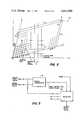
- FIG. 1is a block and schematic diagram of a system embodying the present invention
- FIG. 1Ais a diagrammatic representation of a digital screen illustrating certain principles of the present invention
- FIG. 1Bis a diagrammatic representation of the transformation of the XY into the X'Y' coordinate system
- FIG. 2is a diagrammatic representation of the screen cell of FIG. 1A;
- FIG. 3is a diagrammatic representation of the address generation taught by the present invention.
- FIG. 4is detailed block and schematic diagram of the address generation of FIG. 3;
- FIG. 5is a block and schematic diagram of the digital comparator and selector of FIG. 1;
- FIG. 6is a schematic diagram illustrating the scanning of the screen cell of FIG. 2.
- FIG. 7is a schematic illustration of density values in the screen cell of FIG. 1A.
- System 10includes a scanner 14 which optically scans image 12 and generates image signals that are sensed by an image sensor 16. Under the command of a processor 18, optical density image signals representing variations in optical density of image 12 generated by image sensor 16 and digital screen signals generated by a screen generator 20 are compared in a comparator 22. The digital screen signals represent a screen having a selected optical density pattern. Output data signals, which define the type of image that is to be reproduced, are presented at the output of a selector 24 which receives input signals from comparator 22 and image sensor 16.
- the factors relating to the screen which determine the type of image to be reproducedinclude optical density screen values, screen frequency, screen angle and the printing method ultimately used.
- An increase in screen frequencyimproves resolution of the reproduction.
- Variations in screen angleproduce different effects such as color separation.
- the method and apparatus involving digital screen generation taught by the present inventionapplies to the screening of images whether they be continuous-tone images or bi-level black and white graphics.
- an imageis reproduced in a raster form as a sequence of parallel adjacent lines with a sequence of adjacent picture elements or pixels disposed along each line.
- the teachings of this inventionapply to the generation of screens for continuous-tone screened images used in gravure printing and bi-level half-tone images used in lithographic, relief and electrographic printing.
- the screens generatedhave parallel lines of symmetry in two dimensions.
- FIG. 1Athere is shown a large area image screen 26 which is generated by the repetition of a screen cell 28 in directions a and b, the screen cell having a selected optical density pattern.
- cell 28which is represented by the area denoted OGHI, is defined by a plurality of unique address locations, each address characterized by a selected optical density value.
- screen cell area OGHIis the area included between two adjacent parallel lines in the direction a and two adjacent parallel lines in the direction b.
- Screen 26is formed by the repetition of screen cell 28 in the direction a and in the direction b, the details of the screen cell 28 being shown in FIG. 2.
- FIGS. 1A and 2The parameters denoted in FIGS. 1A and 2 are defined as follows: ##EQU1##
- Screen cell 28is subdivided into a screen cell matrix 30, the size of the matrix being N a by N b in the a and b directions, respectively.
- a positive photographic image of the screen itselfwithout any other image exposure, produces an optical density measurement of the screen at each one of the matrix cell 30 positions.
- the value of this optical densityis stored in a memory array 32 of size N a N b . Since screen 26 is merely the repetition of one screen cell 28, the density of the screen at any point in the image area is defined by the density value at corresponding address locations in memory 32. That is, by suitably addressing memory array 32, it is possible to assign a density value for each point in the image area using screen 26.
- the memory array 32 addressis incremented by the change of address A a per pixel ( ⁇ A ap ) and the change of address A b per pixel ( ⁇ A bp ), the contents of that location in the memory array 32 defines the effective density of the screen along a scan line. If the memory array 32 address is incremented by the change of address A a per line ( ⁇ A al ) and the change of address A b per line ( ⁇ A bl ), then the value of the screen on subsequent lines is determined.
- FIG. 4A specific implementation of this address generation mechanism is shown diagrammatically in FIG. 4.
- the address A a and address A b computationsare essentially identical and are shown on the left-hand and right-hand sides of the dotted line in FIG. 4. The following is directed to the left-hand side (the computation of A a ), but it will be readily appreciated that it applies equally to the computation of A b .
- the four ⁇ valuesare computed from the desired values of screen frequency and screen angle in a microcomputer 36 and those values are shown being transmitted from the microcomputer to registers 38 and 40.
- the first address of the line which is stored in a register 42is cleared to zero.
- the l inputs of multiplexers 44 and 46are selected and a new first address of the line is computed by adding in an accumulator 48 the current first address of the line to ⁇ A l and restoring the first address of line register 42 to the new value.
- the p inputs of multiplexers 44 and 46are selected and the current address stored in accumulator 48 is incremented by ⁇ A p at each pixel.
- the size of the screen cell matrixis 256 (the values of N a and N b ).
- the computation of the addresshas a 24-bit precision.
- the high order 8-bits of A a and A b generated from a register 50, which is gated by a clock 52,are used as the addresses of the screen cell memory array 32.
- the precision of the screen cell matrix computationis one part in 2 16 which allows accurate screen generation over very large images.
- the screen cell memory array address computationoverflows, but this is inconsequential since the screen is modulo 256.
- the value of the contents at each address location in memory array 32represents the effective density of the screen at the address location corresponding to the address location of the pixel in the image.
- the digital value of the actual pixel at each location in the imageis compared in a comparator 54 to the screen values stored in memory array 32 at corresponding locations.
- a selector 56receives the signal from comparator 54 and generates output data signals which define the image to be reproduced. If the image value is greater than the matrix cell value, the output data signals from selector 56 are dependent upon the type of screen that is to be produced. In the case of a halftone screen, the output data value is set to a maximum or black pixel. In the case of a gravure screen, the value of the output pixel is set to be equal to the image pixel tone value thereby generating a screened continuous-tone image that can be used in etching of gravure printing cylinders. A chaining effect is obtained by having the cells touch at 20% of the maximum density in the X direction and at 30% of the maximum density in the Y direction.
- FIG. 6shows the scanning sequence of an individual screen cell 28 in order to provide the optical density values at selected address locations of digital screen 26 for comparison with the actual pixel at corresponding locations in the image.
- the intersection of a scan line and boundary of screen cell 28determines the starting point of the next scan line which is on the opposite boundary. That is, the starting point of scan line II on the lower boundary of screen cell 28 is opposite the intersection of scan line I on the upper boundary of the screen cell.
- FIG. 7is a partial map of the density values of a typical screen cell 28 and shows a substantially sinusoidal profile. In the illustrated embodiment, by way of example, screen cell 28 is symmetrical about its center. In an alternate embodiment, screen cell 28 is not symmetrical about its center.
Landscapes
- Engineering & Computer Science (AREA)
- Multimedia (AREA)
- Signal Processing (AREA)
- Image Processing (AREA)
Abstract
Description
Claims (9)
Priority Applications (1)
| Application Number | Priority Date | Filing Date | Title |
|---|---|---|---|
| US06/295,573US4413286A (en) | 1981-08-24 | 1981-08-24 | Method and apparatus involving digital screen generation |
Applications Claiming Priority (1)
| Application Number | Priority Date | Filing Date | Title |
|---|---|---|---|
| US06/295,573US4413286A (en) | 1981-08-24 | 1981-08-24 | Method and apparatus involving digital screen generation |
Publications (1)
| Publication Number | Publication Date |
|---|---|
| US4413286Atrue US4413286A (en) | 1983-11-01 |
Family
ID=23138279
Family Applications (1)
| Application Number | Title | Priority Date | Filing Date |
|---|---|---|---|
| US06/295,573Expired - Fee RelatedUS4413286A (en) | 1981-08-24 | 1981-08-24 | Method and apparatus involving digital screen generation |
Country Status (1)
| Country | Link |
|---|---|
| US (1) | US4413286A (en) |
Cited By (22)
| Publication number | Priority date | Publication date | Assignee | Title |
|---|---|---|---|---|
| US4486788A (en)* | 1981-04-14 | 1984-12-04 | Dainippon Screen Seizo Kabushiki Kaisha | Method for producing a halftone plate for use in a picture reproducing machine |
| DE3609252A1 (en)* | 1985-03-20 | 1986-10-02 | Canon K.K., Tokio/Tokyo | METHOD AND DEVICE FOR IMAGE REPRODUCTION |
| US4692879A (en)* | 1984-02-09 | 1987-09-08 | Dainippon Screen Mfg. Co., Ltd. | Method of and apparatus for forming the address signals of a screen memory of a half tone dot generator |
| EP0341666A3 (en)* | 1988-05-13 | 1990-02-07 | Yamatoya & Co., Ltd. | Tonal conversion method for pictures |
| US4942480A (en)* | 1988-09-06 | 1990-07-17 | Nynex Corporation | Reproduction of halftone original with moire reduction and tone adjustment |
| US4985779A (en)* | 1989-09-19 | 1991-01-15 | Intergraph Corporation | Improved method and apparatus for generating halftone images |
| WO1992002101A1 (en)* | 1990-07-18 | 1992-02-06 | Linotype Ag | Process for the generation and storage of digitized threshold density values for the scanning of a half-tone image pattern |
| US5187594A (en)* | 1990-02-09 | 1993-02-16 | Graphic Edge, Inc. | Method of creating and applying half tone screen patterns |
| EP0531129A3 (en)* | 1991-09-03 | 1993-03-31 | Raphael L. Levien | Screen generation for halftone screening of images |
| US5204916A (en)* | 1991-08-06 | 1993-04-20 | Eastman Kodak Company | Tile-oriented technique for collectively performing image rotation, scaling and digital halftone screening |
| EP0540169A1 (en)* | 1991-09-27 | 1993-05-05 | Raphael L. Levien | Screen generation for halftone screening of images |
| US5315406A (en)* | 1991-09-03 | 1994-05-24 | Levien Raphael L | Screen generation for halftone screening of images using arbitrary distribution of transformed screen coordinates |
| US5442461A (en)* | 1991-09-03 | 1995-08-15 | Levien; Raphael L. | Screen generation for halftone screening of images with reduction of irrational correction artifacts |
| US5463720A (en)* | 1992-09-28 | 1995-10-31 | Granger; Edward M. | Blue noise based technique for use in a halftone tile oriented screener for masking screener induced image artifacts |
| US5471543A (en)* | 1990-06-25 | 1995-11-28 | Eastman Kodak Company | Mixed screen frequencies with image segmentation |
| US5515182A (en)* | 1992-08-31 | 1996-05-07 | Howtek, Inc. | Rotary scanner |
| US5537223A (en)* | 1994-06-02 | 1996-07-16 | Xerox Corporation | Rotating non-rotationally symmetrical halftone dots for encoding embedded data in a hyperacuity printer |
| US5642436A (en)* | 1990-07-18 | 1997-06-24 | Linotype-Hell Ag | Method for generating and storing digitalized density threshold values for the rastering of a half-tone picture original |
| US5689623A (en)* | 1995-03-27 | 1997-11-18 | Optronics International Corporation | Spread spectrum digital screening |
| US5805171A (en)* | 1996-07-19 | 1998-09-08 | Van Houten Technologies, Inc. | Technical schematic display system utilizing preassigned component detail levels |
| US5815243A (en)* | 1993-02-10 | 1998-09-29 | Agfa Division, Bayer Corporation | Electronic prepress apparatus for producing lithographic printing plates |
| US7085017B1 (en) | 2001-08-03 | 2006-08-01 | Elesys, Inc. | Polar halftone methods for radial printing |
Citations (2)
| Publication number | Priority date | Publication date | Assignee | Title |
|---|---|---|---|---|
| US4149194A (en)* | 1977-07-07 | 1979-04-10 | Xerox Corporation | Variable angle electronic halftone screening |
| US4350996A (en)* | 1980-04-14 | 1982-09-21 | Scitex Corporation Ltd. | Screened image reproduction |
- 1981
- 1981-08-24USUS06/295,573patent/US4413286A/ennot_activeExpired - Fee Related
Patent Citations (2)
| Publication number | Priority date | Publication date | Assignee | Title |
|---|---|---|---|---|
| US4149194A (en)* | 1977-07-07 | 1979-04-10 | Xerox Corporation | Variable angle electronic halftone screening |
| US4350996A (en)* | 1980-04-14 | 1982-09-21 | Scitex Corporation Ltd. | Screened image reproduction |
Cited By (26)
| Publication number | Priority date | Publication date | Assignee | Title |
|---|---|---|---|---|
| US4486788A (en)* | 1981-04-14 | 1984-12-04 | Dainippon Screen Seizo Kabushiki Kaisha | Method for producing a halftone plate for use in a picture reproducing machine |
| US4692879A (en)* | 1984-02-09 | 1987-09-08 | Dainippon Screen Mfg. Co., Ltd. | Method of and apparatus for forming the address signals of a screen memory of a half tone dot generator |
| DE3609252A1 (en)* | 1985-03-20 | 1986-10-02 | Canon K.K., Tokio/Tokyo | METHOD AND DEVICE FOR IMAGE REPRODUCTION |
| US4814886A (en)* | 1985-03-20 | 1989-03-21 | Canon Kabushiki Kaisha | Image processing process and apparatus therefor |
| EP0341666A3 (en)* | 1988-05-13 | 1990-02-07 | Yamatoya & Co., Ltd. | Tonal conversion method for pictures |
| US4942480A (en)* | 1988-09-06 | 1990-07-17 | Nynex Corporation | Reproduction of halftone original with moire reduction and tone adjustment |
| US4985779A (en)* | 1989-09-19 | 1991-01-15 | Intergraph Corporation | Improved method and apparatus for generating halftone images |
| US5187594A (en)* | 1990-02-09 | 1993-02-16 | Graphic Edge, Inc. | Method of creating and applying half tone screen patterns |
| US5471543A (en)* | 1990-06-25 | 1995-11-28 | Eastman Kodak Company | Mixed screen frequencies with image segmentation |
| WO1992002101A1 (en)* | 1990-07-18 | 1992-02-06 | Linotype Ag | Process for the generation and storage of digitized threshold density values for the scanning of a half-tone image pattern |
| JP2891775B2 (en) | 1990-07-18 | 1999-05-17 | ハイデルベルガー ドルツクマシーネン アクチエンゲゼルシヤフト | Digitized density limit generation and storage method for halftone original image mesh screen |
| US5642436A (en)* | 1990-07-18 | 1997-06-24 | Linotype-Hell Ag | Method for generating and storing digitalized density threshold values for the rastering of a half-tone picture original |
| US5204916A (en)* | 1991-08-06 | 1993-04-20 | Eastman Kodak Company | Tile-oriented technique for collectively performing image rotation, scaling and digital halftone screening |
| US5307181A (en)* | 1991-09-03 | 1994-04-26 | Levien Raphael L | Screen generation for halftone screening of images using scan line segments of oversized screen scan lines |
| US5442461A (en)* | 1991-09-03 | 1995-08-15 | Levien; Raphael L. | Screen generation for halftone screening of images with reduction of irrational correction artifacts |
| US5315406A (en)* | 1991-09-03 | 1994-05-24 | Levien Raphael L | Screen generation for halftone screening of images using arbitrary distribution of transformed screen coordinates |
| EP0531129A3 (en)* | 1991-09-03 | 1993-03-31 | Raphael L. Levien | Screen generation for halftone screening of images |
| EP0540169A1 (en)* | 1991-09-27 | 1993-05-05 | Raphael L. Levien | Screen generation for halftone screening of images |
| US5515182A (en)* | 1992-08-31 | 1996-05-07 | Howtek, Inc. | Rotary scanner |
| US5463720A (en)* | 1992-09-28 | 1995-10-31 | Granger; Edward M. | Blue noise based technique for use in a halftone tile oriented screener for masking screener induced image artifacts |
| US5815243A (en)* | 1993-02-10 | 1998-09-29 | Agfa Division, Bayer Corporation | Electronic prepress apparatus for producing lithographic printing plates |
| US5537223A (en)* | 1994-06-02 | 1996-07-16 | Xerox Corporation | Rotating non-rotationally symmetrical halftone dots for encoding embedded data in a hyperacuity printer |
| US5689623A (en)* | 1995-03-27 | 1997-11-18 | Optronics International Corporation | Spread spectrum digital screening |
| US5805171A (en)* | 1996-07-19 | 1998-09-08 | Van Houten Technologies, Inc. | Technical schematic display system utilizing preassigned component detail levels |
| US7085017B1 (en) | 2001-08-03 | 2006-08-01 | Elesys, Inc. | Polar halftone methods for radial printing |
| US20060238813A1 (en)* | 2001-08-03 | 2006-10-26 | Elesys, Inc. | Polar halftone methods for radial printing |
Similar Documents
| Publication | Publication Date | Title |
|---|---|---|
| US4413286A (en) | Method and apparatus involving digital screen generation | |
| US4339774A (en) | Apparatus and method for generating a dispersed dot half tone picture from a continuous tone picture | |
| US4987498A (en) | Method of forming halftone screen | |
| US4651287A (en) | Digital image processing algorithm for output devices with discrete halftone gray scale capability | |
| EP0201674B1 (en) | A method for reproducing multi-level digital images on a bi-level printer of fixed dot size | |
| US4630125A (en) | Unscreening of stored digital halftone images | |
| US4149194A (en) | Variable angle electronic halftone screening | |
| US4626901A (en) | Image processing apparatus using multiple dither matrices | |
| US5202772A (en) | Color halftone screen utilizing preselected halftone dots placed at preselected distance and screen angles from center halftone dots | |
| US4246614A (en) | Binary graphic printer system having an electronic screen with shift control suited for rescreening | |
| JP3366655B2 (en) | Halftone image generating method and its screen device | |
| US5515456A (en) | Process for providing digital halftone image with random error diffusion, color correction and enlargement | |
| GB2133948A (en) | Generating screened half-tone images | |
| US5140431A (en) | Digital electronic system for halftone printing | |
| US3961132A (en) | Sequential image-modulated dot-area recording | |
| EP0342845B1 (en) | Producing half-tone images | |
| US5663810A (en) | Method and apparatus for producing a digital half-tone representation of an image | |
| US4773734A (en) | Method of forming halftone screen | |
| US5184213A (en) | Binarizing method for color image using modified error diffusion method | |
| US5107331A (en) | Method and apparatus for producing half-tone separations at the same screen angle | |
| US5264926A (en) | Perpendicular, equal frequency non-conventional screen patterns for electronic halftone generation | |
| EP0585962A1 (en) | Halftone gradation image signal generating apparatus | |
| EP0418844B1 (en) | Color image information processing method | |
| JPH0550187B2 (en) | ||
| US5600448A (en) | Apparatus and method for generating a screened reproduction of an image |
Legal Events
| Date | Code | Title | Description |
|---|---|---|---|
| AS | Assignment | Owner name:OPTRONICS INTERNATIONAL, INC., 7 STUART ROAD, CHEL Free format text:ASSIGNMENT OF ASSIGNORS INTEREST.;ASSIGNOR:BOSTON, WILLIAM T.;REEL/FRAME:003913/0046 Effective date:19810810 Owner name:OPTRONICS INTERNATIONAL, INC., MASSACHUSETTS Free format text:ASSIGNMENT OF ASSIGNORS INTEREST;ASSIGNOR:BOSTON, WILLIAM T.;REEL/FRAME:003913/0046 Effective date:19810810 | |
| AS | Assignment | Owner name:KLIMSCH/OPTRONICS, INC., SEVEN STUART ROAD, CHELMS Free format text:ASSIGNMENT OF ASSIGNORS INTEREST.;ASSIGNOR:OPTRONICS INTERNATIONAL, INC.;REEL/FRAME:004362/0301 Effective date:19850116 | |
| MAFP | Maintenance fee payment | Free format text:PAYMENT OF MAINTENANCE FEE, 4TH YEAR, PL 96-517 (ORIGINAL EVENT CODE: M170); ENTITY STATUS OF PATENT OWNER: LARGE ENTITY Year of fee payment:4 | |
| AS | Assignment | Owner name:INTERGRAPH CORPORATION, ONE MADISON INDUSTRIAL PAR Free format text:ASSIGNMENT OF ASSIGNORS INTEREST.;ASSIGNOR:OPTRONICS INTERNATIONAL, INC., A CORP. OF MA;REEL/FRAME:004918/0695 Effective date:19880630 | |
| FEPP | Fee payment procedure | Free format text:MAINTENANCE FEE REMINDER MAILED (ORIGINAL EVENT CODE: REM.); ENTITY STATUS OF PATENT OWNER: LARGE ENTITY | |
| LAPS | Lapse for failure to pay maintenance fees | ||
| FP | Lapsed due to failure to pay maintenance fee | Effective date:19911103 | |
| AS | Assignment | Owner name:CITICORP USA, INC., NEW YORK Free format text:SECURITY AGREEMENT;ASSIGNOR:INTERGRAPH CORPORATION;REEL/FRAME:007662/0422 Effective date:19951006 | |
| AS | Assignment | Owner name:FOOTHILL CAPITAL CORPORATION, CALIFORNIA Free format text:SECURITY INTEREST;ASSIGNOR:INTERGRAPH CORPORATION;REEL/FRAME:008239/0350 Effective date:19961220 | |
| AS | Assignment | Owner name:INTERGRAPH CORPORATION, ALABAMA Free format text:TERMINATION AND RELEASE;ASSIGNOR:CITICORP USA, INC.;REEL/FRAME:008454/0190 Effective date:19970106 | |
| AS | Assignment | Owner name:INTERGRAPH CORPORATION, ALABAMA Free format text:TERMINATION AND RELEASE;ASSIGNOR:FOOTHILL CAPITAL CORPORATION;REEL/FRAME:008442/0147 Effective date:19970317 Owner name:OPTRONICS INTERNATIONAL CORPORATION, MASSACHUSETTS Free format text:ASSIGNMENT OF ASSIGNORS INTEREST;ASSIGNOR:INTERGRAPH CORPORATION;REEL/FRAME:008447/0070 Effective date:19970314 | |
| AS | Assignment | Owner name:ECRM INCORPORATED, MASSACHUSETTS Free format text:ASSIGNMENT OF ASSIGNORS INTEREST;ASSIGNOR:OPTRONICS INTERNATIONAL CORPORATION;REEL/FRAME:010710/0001 Effective date:20000303 | |
| AS | Assignment | Owner name:ECRM INCORPORATED, MASSACHUSETTS Free format text:ASSIGNMENT OF ASSIGNORS INTEREST;ASSIGNOR:OPTRONICS INTERNATIONAL CORPORATION;REEL/FRAME:011967/0760 Effective date:20000303 | |
| STCH | Information on status: patent discontinuation | Free format text:PATENT EXPIRED DUE TO NONPAYMENT OF MAINTENANCE FEES UNDER 37 CFR 1.362 |