US4412337A - Power amplifier and envelope correction circuitry - Google Patents
Power amplifier and envelope correction circuitryDownload PDFInfo
- Publication number
- US4412337A US4412337AUS06/318,281US31828181AUS4412337AUS 4412337 AUS4412337 AUS 4412337AUS 31828181 AUS31828181 AUS 31828181AUS 4412337 AUS4412337 AUS 4412337A
- Authority
- US
- United States
- Prior art keywords
- envelope
- pulse
- output
- amplifier
- preferred
- Prior art date
- Legal status (The legal status is an assumption and is not a legal conclusion. Google has not performed a legal analysis and makes no representation as to the accuracy of the status listed.)
- Expired - Lifetime
Links
- 238000012937correctionMethods0.000titleclaimsdescription21
- NJPPVKZQTLUDBO-UHFFFAOYSA-NnovaluronChemical compoundC1=C(Cl)C(OC(F)(F)C(OC(F)(F)F)F)=CC=C1NC(=O)NC(=O)C1=C(F)C=CC=C1FNJPPVKZQTLUDBO-UHFFFAOYSA-N0.000claimsdescription12
- 101100536250Homo sapiens TMEM120A geneProteins0.000claimsdescription11
- 102100028548Ion channel TACANHuman genes0.000claimsdescription11
- 230000015654memoryEffects0.000claimsdescription11
- 238000000034methodMethods0.000claimsdescription8
- 238000003860storageMethods0.000claimsdescription6
- 230000005669field effectEffects0.000claimsdescription3
- 238000001914filtrationMethods0.000claims1
- 230000006870functionEffects0.000description37
- 238000012546transferMethods0.000description16
- 239000003990capacitorSubstances0.000description7
- 230000008859changeEffects0.000description5
- 238000010586diagramMethods0.000description5
- 230000004044responseEffects0.000description5
- 238000001228spectrumMethods0.000description5
- 230000003111delayed effectEffects0.000description4
- 238000012986modificationMethods0.000description4
- 230000004048modificationEffects0.000description4
- 238000013459approachMethods0.000description3
- 230000008901benefitEffects0.000description3
- 238000012545processingMethods0.000description3
- 230000008878couplingEffects0.000description2
- 238000010168coupling processMethods0.000description2
- 238000005859coupling reactionMethods0.000description2
- 230000000694effectsEffects0.000description2
- 238000004519manufacturing processMethods0.000description2
- 238000005070samplingMethods0.000description2
- 239000004065semiconductorSubstances0.000description2
- 230000009471actionEffects0.000description1
- 230000002411adverseEffects0.000description1
- 230000005540biological transmissionEffects0.000description1
- 230000006835compressionEffects0.000description1
- 238000007906compressionMethods0.000description1
- 238000013461designMethods0.000description1
- 230000006872improvementEffects0.000description1
- 230000008569processEffects0.000description1
- 230000000630rising effectEffects0.000description1
- 230000035945sensitivityEffects0.000description1
- 230000007480spreadingEffects0.000description1
- 238000003892spreadingMethods0.000description1
Images


Classifications
- H—ELECTRICITY
- H03—ELECTRONIC CIRCUITRY
- H03F—AMPLIFIERS
- H03F1/00—Details of amplifiers with only discharge tubes, only semiconductor devices or only unspecified devices as amplifying elements
- H03F1/32—Modifications of amplifiers to reduce non-linear distortion
- H03F1/3241—Modifications of amplifiers to reduce non-linear distortion using predistortion circuits
- H03F1/3247—Modifications of amplifiers to reduce non-linear distortion using predistortion circuits using feedback acting on predistortion circuits
- H—ELECTRICITY
- H03—ELECTRONIC CIRCUITRY
- H03F—AMPLIFIERS
- H03F1/00—Details of amplifiers with only discharge tubes, only semiconductor devices or only unspecified devices as amplifying elements
- H03F1/32—Modifications of amplifiers to reduce non-linear distortion
- H03F1/3241—Modifications of amplifiers to reduce non-linear distortion using predistortion circuits
- H03F1/3276—Modifications of amplifiers to reduce non-linear distortion using predistortion circuits using the nonlinearity inherent to components, e.g. a diode
- H—ELECTRICITY
- H03—ELECTRONIC CIRCUITRY
- H03F—AMPLIFIERS
- H03F1/00—Details of amplifiers with only discharge tubes, only semiconductor devices or only unspecified devices as amplifying elements
- H03F1/34—Negative-feedback-circuit arrangements with or without positive feedback
- H—ELECTRICITY
- H03—ELECTRONIC CIRCUITRY
- H03F—AMPLIFIERS
- H03F3/00—Amplifiers with only discharge tubes or only semiconductor devices as amplifying elements
- H03F3/20—Power amplifiers, e.g. Class B amplifiers, Class C amplifiers
- H03F3/24—Power amplifiers, e.g. Class B amplifiers, Class C amplifiers of transmitter output stages
- H—ELECTRICITY
- H03—ELECTRONIC CIRCUITRY
- H03F—AMPLIFIERS
- H03F2200/00—Indexing scheme relating to amplifiers
- H03F2200/198—A hybrid coupler being used as coupling circuit between stages of an amplifier circuit
- H—ELECTRICITY
- H03—ELECTRONIC CIRCUITRY
- H03F—AMPLIFIERS
- H03F2201/00—Indexing scheme relating to details of amplifiers with only discharge tubes, only semiconductor devices or only unspecified devices as amplifying elements covered by H03F1/00
- H03F2201/32—Indexing scheme relating to modifications of amplifiers to reduce non-linear distortion
- H03F2201/3227—Adaptive predistortion based on amplitude, envelope or power level feedback from the output of the main amplifier
- H—ELECTRICITY
- H03—ELECTRONIC CIRCUITRY
- H03F—AMPLIFIERS
- H03F2201/00—Indexing scheme relating to details of amplifiers with only discharge tubes, only semiconductor devices or only unspecified devices as amplifying elements covered by H03F1/00
- H03F2201/32—Indexing scheme relating to modifications of amplifiers to reduce non-linear distortion
- H03F2201/3233—Adaptive predistortion using lookup table, e.g. memory, RAM, ROM, LUT, to generate the predistortion
- H—ELECTRICITY
- H04—ELECTRIC COMMUNICATION TECHNIQUE
- H04B—TRANSMISSION
- H04B1/00—Details of transmission systems, not covered by a single one of groups H04B3/00 - H04B13/00; Details of transmission systems not characterised by the medium used for transmission
- H04B1/02—Transmitters
- H04B1/04—Circuits
- H04B2001/0408—Circuits with power amplifiers
- H04B2001/0433—Circuits with power amplifiers with linearisation using feedback
Definitions
- the present inventionpertains to a power amplifier and envelope correction circuitry associated therewith.
- Power amplifiersand especially semiconductor power amplifiers, can be very non-linear so that providing a preferred pulse envelope at the output thereof is extremely difficult. This is especially true if the duty cycle, or sequence, of a pulse train is not constant. Further, in many applications the peak pulse power may be relatively large so that temperature changes and the like within the circuitry of the power amplifier have a substantial and adverse effect.
- TACAN ground station transponderswhich provide distance, azimuth, and station identification information to properly equipped aircraft, must be capable of producing pulse trains wherein the time between pulses varies radically but the amplitude and shape of the pulses is closely controlled.
- the shape of the pulseshould be a smooth bell curve, or Gaussian wave form, to minimize the frequency spectrum occupied by the radiated energy so as not to interfere with adjacent channels in the TACAN system. Any variations in the shape of the output pulse may cause spectrum spreading, and may result in interference with adjacent TACAN channels. Any variations in the amplitude of the output pulse may cause erroneous navigational information.
- the output pulse shape and amplitudeis controlled with an analog loop around the power amplifier.
- the components of these circuitshave many parts with carefully controlled values, and are expensive and difficult to manufacture. Further, to reduce the requirements of the analog loop the power amplifier must be constructed as linear as possible. Since the power amplifier, in a TACAN system for example, is an RF amplifier, the components are RF devices which are generally expensive and difficult to manufacture.
- TACAN navigational systemis utilized herein as a specific example, it will be understood by those skilled in the art that a great variety of applications exist wherein precise control of the output of a nonlinear amplifier is required. Further, while a power amplifier is specified it will be clear to those skilled in the art that the present envelope correction circuitry can be manufactured independent of the amplifier.
- the present inventionpertains to envelope correction circuitry for use with a power amplifier, which circuitry includes envelope generating apparatus for generating a preferred envelope, a comparator coupled to sense the output of the power amplifier and compare the preferred envelope thereto, circuitry for utilizing the comparison to generate a predistorted envelope and modulating circuitry coupled to the input of the amplifier for modulating the input thereto with the predistorted envelope so that output pulses from the power amplifier have substantially the preferred envelope.
- K oa constant chosen for a specific rise time.
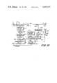
- FIG. 1is a simplified block diagram of a power amplifier and envelope correction circuitry incorporating the present invention
- FIGS. 2, A and Billustrate the time domain and frequency domain, respectively, of a preferred pulse envelope for use in the circuitry of FIG. 1;
- FIG. 3is the curve of a typical transfer function for a semiconductor type Class C power amplifier
- FIG. 4illustrates a series of output waveforms present in the envelope correction circuitry of FIG. 1;
- FIG. 5generally illustrates the waveform of compensating circuitry incorporated in the circuitry of FIG. 1;
- FIG. 6is schematic diagram of a detector utilized in the circuitry of FIG. 1;
- FIG. 7is a schematic diagram of a non-linear network utilized in the circuitry of FIG. 1;
- FIG. 8is a typical waveform of the attenuation curve for a pin diode reflection modulator utilized in FIG. 1;
- FIG. 9illustrates a pair of curves representing power amplifier RF output versus modulator control voltage with linear and reflective corrector modulators
- FIG. 10is a schematic diagram of a typical reflective pin diode modulator
- FIG. 11illustrates four curves representing incremental gain versus four different reflective corrector constants
- FIG. 12is the block diagram of another embodiment of a power amplifier and envelope correction circuitry utilizing the present invention.
- FIG. 1a power amplifier and envelope correction circuit incorporating the present invention is illustrated. It will be understood by those skilled in the art that the circuitry illustrated in FIG. 1 is specifically adapted for use in a TACAN navigation system and some minor modifications may be required for other applications.
- An input terminal, designated 10is designed to receive an RF signal from a source not shown. The RF at the terminal 10 is applied to one input of a first modulator 12. The output of the modulator 12 is supplied to a first input of a second modulator, generally designated 15, which includes an amplifier 16 and a pin diode reflective modulator 17. The output of the second modulator 15 is applied to the input of a power amplifier 20.
- the output of the power amplifier 20is connected through a low pass filter 22 and a circulator circuit 23 to an RF output terminal 25.
- a coupling device 30,which in this embodiment is illustrated as a directional coupler, couples a small amount of the energy at the output of the low pass filter 22 to a detector 32.
- the detector 32essentially follows the peak carrier level so that only the envelope of the output pulses from the low pass filter 22 is available at the output of the detector 32.
- the pulse envelope at the output of the detector 32is supplied to an input of a comparator 35, a resistor 36, and a non-linear network 39.
- the comparator 35has a second input with a fixed voltage, V 1 , supplied thereto. The voltage V 1 will be explained presently.
- the output of the nonlinear network 39is applied to one input of a summing amplifier or comparator circuit 41.
- the output of the summing amplifier 41is supplied through a controlled resistance, 37 having its resistance value control derived from a control network 38 to the input of an integrator 43.
- the output of the integrator 43is supplied to an input of a summing circuit generally designated 45, through a resistor 46 to a second input of the first modulator 12, and to the input of a sample and hold circuit 48.
- the integrator 43is part of an analog feedback circuit around the power amplifier 20, which circuit is capable of correcting minor errors in the output pulses.
- a reference read-only memory (ROM) 50has a preferred pulse envelope stored therein in digital form.
- an address generator and control circuit 53causes the reference ROM 50 to supply digital signals to a digital-to-analog converter 55.
- the combination of the ROM 50 and the converter 55provide a preferred pulse envelope in analog form through a low pass filter 56 and a non-linear network 57 to a second input of the summing amplifier 41.
- the summing amplifier 41subtracts the output pulse envelope supplied by the detector 32 and non-linear network 39 from the preferred pulse envelope supplied by the ROM 50 and non-linear network 57. The difference between the two pulses is supplied through the controlled resistance 37 to the integrator 43 and appears at the output thereof as an error signal.
- the output of the summing circuit 45is applied to the input of an amplifier 60, the output of which is connected to a second input of the second modulator 15, and to the input of the an analog-to-digital converter 62.
- the output of the analog-to-digital converter 62is connected to a switching circuit 65.
- the switching circuit 65has a pair of outputs connected to first and second random access memories 66 and 67, respectively. The switching is accomplished such that memories 66 and 67 alternate roles as input or output memories on alternate pulses.
- a switching circuit 70is connected to memories 66 and 67 to supply control signals thereto from address generator and control 53.
- control signalsWhen the control signals are routed to either of the memories 66 or 67 as an input, they are delayed by delay network 69, however control signals routed to an output memory 66 or 67 are not delayed.
- the control signalsare generated upon receipt of an input trigger on terminal 52.
- a control signalis also supplied to a hold input of the sample and hold circuit 48.
- the output of the switching circuit 65is supplied through a digital-to-analog converter 72 and low pass filter 73 to a second input of the summing circuit 45 and through a resistor 75 to the second input of the first modulator 12.
- the signal supplied to the second input of the first modulator 12is a corrected predistorted pulse envelope which, when applied to the power amplifier 20 produces the desired or preferred pulse at the output thereof.
- a capacitor 85is connected between the input and output of the integrator 43.
- a transmission gate 86operates at a specific time to connect a resistor 87 in parallel with the capacitor 85 to reduce the integrator gain during the off period.
- the output of the comparator 35is applied to one input of a function generator 90, the output of which is supplied to the input of the integrator 43.
- the function generator 90 and the gate 86operates in response to signals from the address generator and control 53.
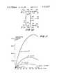
- the power amplifier 20has a transfer function generally as illustrated by the curve in FIG. 3. It can be seen that this transfer function is very non-linear with the first portion thereof remaining at substantially 0 out to a first point, designated 1, and then rising relatively slowly to a second point, designated 2, after which the curve rises sharply for a relatively long section before again leveling off. It will of course be understood that if other power amplifiers are utilized they may have a somewhat different transfer function and some of the compensating circuits described herein may require slight modifications, or may not be required.
- the preferred pulse envelope stored in the reference ROM 50is illustrated in FIG. 2A.
- the curve as actually stored in the reference ROM 50is represented by a plurality of samples (for example 128) with the curve being truncated where it crosses the zero axis (the first time) at either side of the center of the curve.
- the frequency responsewill be generally as illustrated in FIG. 2B.
- the frequency responsedrops off very sharply so that no signals (frequencies) are produced which will interfere with adjacent channels or the like. The reason that no interference occurs is because of the novel curve being utilized. Because the curve is generated digitally, practical limitations on the number of digital samples used dictate that the curve must be terminated, or truncated, at upper and lower limits.
- the comparator 35 and function generator 90provide a portion of the compensation required.
- the comparator 35is designed to provide an output when the voltage at the output of the detector 32 begins to rise above 0 (Point 1 in FIG. 3). In the present embodiment this is approximately 10 millivolts.
- the address generator and control circuit 53supplies a set signal to the function generator 90 at the start of each pulse.
- FIG. 5is a waveform of the output of the function generator 90 and a sharp drop or step function is illustrated at time T 1 when the set pulse is applied thereto by the address generator and control circuit 53.
- FIG. 4illustrates a set of four error signals as they appear at the output of the integrator 43.
- the four pulsesare illustrated in vertical alignment to show the timing, but it will be understood by those skilled in the art that the pulses appear sequentially with pulse 1 appearing first and then pulse 2, etc.
- each of the error signalsstarts with a pedestal, which pedestal is formed by the set/reset pulse of the function generator 90.
- the pedestalscan be seen in FIG. 4 between the times T 1 and T 2 .
- the function generator 90is constructed so that upon receiving a reset pulse the set function actually goes beyond the normal voltage and returns a very short time later, T 3 , to normal.
- This over-shootis intentionally designed in the function generator 90 to compensate for forward delay in the circuit between the output of the power amplifier and the summing amplifier 41.
- the voltage excursionis so small that it is virtually undetectable in the error signals of FIG. 4.
- the waveform generated by the function generator 90 and integrated by the integrator 43is applied to the sample-and-hold circuit 48 so that the pedestal in the error signal waveforms at the output of the integrator 43 is actually applied negatively to a third input of the summing circuit 45. Because the pedestal is applied negatively it is subtracted from the signal applied to the first input and only the predistored pulse appears at the output of the summing circuit 45. The reasons for this will be apparent presently.
- pulse 1the output of the integrator 43 will appear as pulse 1 in FIG. 4.
- This pulseincludes the pedestal generated by the function generator 90 but otherwise has not had the benefit of being operated upon by the digital feedback circuitry of FIG. 1.
- Pulse 1 at the output of the integrator 43is supplied through the resistor 46 to the first modulator 12 for modulating the next gated pulse of RF input.
- the pulse 1is also supplied to the first input of the summing circuit 45.
- the sample-and-hold circuit 48supplies a pedestal to the third input of the summing circuit 45 so that only the pulse portion of the error signal is applied through the A/D converter 62 and the demultiplexing circuit 65 to the RAM 66 for storage. Since no previous pulses occured there are no pulses stored in the RAMs 66 and 67 and, thus, no signal is applied to the second input of the summing circuit 45.
- the second modulated RF pulseis amplified by the power amplifier 20 and the envelope thereof, from the detector 32, is applied to the summing amplifier 41 along with the preferred pulse from the ROM 50.
- the summing amplifier 41 and integrator 43provide an output signal representative of the errors between the preferred envelope and the actual envelope, which errors (along with the pedestal) appear as pulse 2 in FIG. 4.
- the error signal (pulse 2)is applied through the resistor 46 to the first modulator 12 along with the stored pulse from RAM 66, which is applied through switching circuit 70, converter 72, low pass filter 73 and resistor 75.
- the delay circuit 69provides delay for control signals used by the input RAM. The amount of this delay is identical to the delay through the low pass filter 73.
- the pulse being read out of RAM 66is supplied to the second input of the summing circuit 45, along with the error signals supplied to the first input thereof minus the pedestal supplied to the third input, so that the corrected predistorted pulse is stored in RAM 67 while RAM 66 is reading out the previously stored pulse.
- the pulse stored in RAM 67is then utilized in conjunction with the next error signal (pulse 3 of FIG. 4) to produce the next modulated RF pulse from the first modulator 12 and to supply the next corrected predistorted pulse to RAM 66.
- the digital feedback loopcompares each output pulse to the stored preferred pulse from ROM 50 and utilizes the error signals at the output of the integrator 43, in conjunction with the stored previous predistorted pulse, to generate a corrected predistorted pulse which is in turn utilized to modulate the next RF pulse.
- This combination of analog and digital feedback envelope correction circuitryoperates very rapidly so that only the first pulse in a sequence varies somewhat from the preferred pulse. The amount of variation in the first pulse is determined by the analog portion of the feedback loop and should be substantially unnoticeable in a series of transmitted pulses.
- any non-linearities in the detector 32will affect the feedback loop and, it is an advantage of this approach that the waveforms stored in the ROM 50 can be programmed to compensate for non-linearities of the detector 32, since it is difficult to provide a detector with a very wide linear range.
- the detector 32should be linear over a very wide range, for example, at least 50 db.
- FIG. 6A detector which will fulfil this requirement is illustrated in FIG. 6. Referring specifically to FIG. 6, an input terminal 110 is connected to one side of a resistor 111, the other side of which is grounded, and to one plate of a capacitor 113.
- the opposite plate of the capacitor 113is connected to the cathode of a diode 115, the anode of which is connected to ground and to the anode of a diode 117, the cathode of which is connected to an output terminal 120.
- the cathode of the diode 117is also connected to one plate of a capacitor 121, the other plate of which is grounded and to one side of a current source 123, the other side of which is grounded.
- the detector illustrated in FIG. 6is simply illustrated as an example of a detector having a linear range greater than 50 db and many other detectors can be devised by those skilled in the art.
- the circuitry of FIG. 1is provided with three different gain changing circuits any one of which may be utilized or any combination of which might be utilized to perform the function.
- the three gain changing circuitsare as follows: 1, the second modulator 15 and amplifier 60; 2, control network 38 driving controlled resistor 37; and 3, the non-linear networks 39 and 57.
- the amplifier 60provides a signal to the second modulator 15 when the voltage supplied from the summing circuit 45 exceeds the voltage at the second point on the transfer function of FIG. 3, which is the point at which the power amplifier incremental gain becomes large in this embodiment.
- the second modulator 15contains amplifier 16 which has a gain of 30 and the pin diode reflective modulator 17 that has an incremental gain which can be represented by a hyperbolic function. It was determined that the hyperbolic function of the pin diode reflective modulator 17 is preferred as compared to a linear modulator.
- the reflective pin diode modulator correction circuitcomprised of linear modulator 12, amplifier 16 and pin diode modulator 17 posses a nonlinear transfer function as illustrated in FIG. 8. It is included in the control loop to minimize the loop gain variation over the RF signal dynamic range.
- curve 170illustrates the power amplifier transfer function that results from using only linear modulator 12, compared to the less severe transfer function with more constant slope of curve 171 that results from including amplifier 16 and pin diode modulator 17. The slope of the curve represents incremental loop gain and would ideally be constant (for a linear amplifier).
- FIG. 10illustrates a specific example of pin diode modulator 17.
- a quadrature hybrid coupler 175has an RF input terminal 177, which in FIG. 1 receives an RF signal from amplifier 16, and an RF output terminal 179, which in FIG. 1 supplies the RF output signal to power amplifier 20.
- a third terminal of the coupler 175is connected through a capacitor 180 to a junction 181.
- a fourth terminal of the coupler 175is connected through a capacitor 183 to a junction 184.
- the junction 181is connected through a pin diode 186 and terminating resistor 187 to ground.
- the junction 181is also connected through a series connected inductance 188 and resistor 189 to a control voltage input terminal 190, which in FIG. 1 is connected to the output of comparator 60.
- the junction 184is connected through a pin diode 191 and terminating resistor 192 to ground.
- the junction 184is also connected through a series connected inductance 193 and resistor 194 to
- v 3control voltage at input.
- K dhas been chosen to be equal to 20.
- FIG. 11illustrates the slope or incremental gain variation for several values of K d . With K d equal to 20 the result is a nearly constant gain (curve C in FIG. 11) as compared to the extreme gain variations that result from a high value of K d (e.g. 1 ⁇ 10 6 of curve A) which produce essentially no compensation of the reflective corrector.
- the first gain changing circuitoperates on the RF applied to the power amplifier 20 to alter the amplitude of signals applied thereto so that the loop gain tends to remain constant as the level of an input pulse progresses along the transfer function of the power amplifier 20.
- the second gain changing networkincludes a soft clamp, generally designated 81, connected to receive the detected envelope from the resistor 36 and supply a signal to the control network 38.
- the output of the control network 38is connected to the gate of a field effect transistor (FET) which operates as the voltage controlled resistance 37.
- FETfield effect transistor
- the voltage controlled resistance 37 at the output of the integrator 43enables the gain and bandwidth characteristics of the loop to be adjusted in a continuous manner.
- the control network 38 connected to the detected outputconverts that signal into a control voltage which adjusts the channel resistance of the FET (voltage controlled resistance 37).
- This configurationenables the gain of the loop feedback circuitry to be high while the power amplifier gain is low, which occurs at low power output levels.
- the detected output signalcauses the control network 38 to increase the resistance of the FET to decrease the effective gain of the integrator 43. This process enables the loop gain to be held relatively constant, even though the power amplifier gain varies greatly at varying output levels.
- the "soft" clamp 81sets the upper limit for action of the resistance control network 38 and avoids an abrupt cessation of change in controlled resistor 37 which would produce a step change in incremental gain.
- the third gain changing circuitis the non-linear network 39 positioned between the output of the detector 32 and the summing circuit 41.
- a disadvantage of this circuitis that an identical non-linear network 57 must be placed in the circuit connecting the ROM 50 to the summing amplifier 41 however the networks are closely matched and any residual errors are corrected in the same manner as the non-linearities of the diode detector are, by predistorting the reference pulse.
- a typical non-linear network which may be utilized for the networks 39 and 57is illustrated in FIG. 7.
- An input terminal 150is connected through a resistor 152 to a junction 153.
- the junction 153is connected through a resistor 155 to ground and to the anode of a diode 157.
- the cathode of the diode 157is connected through a resistor 159 to a terminal 160 adapted to have a positive source of voltage (not shown) supplied thereto.
- the junction 153is also connected through a resistor 162 to a second junction 164.
- the junction 164is connected through a resistor 166 to ground and to the anode of a diode 167.
- the cathode of the diode 167is connected through a resistor 169 to the positive junction 160.
- the junction 164serves as the output of the circuit.
- the diodes 157 and 167 of the non-linear networkare connected to turn on as the voltage supplied thereto increases with the diode 157 turning on first and the diode 167 turning on after the voltage increases to a further pre-determined point.
- the non-linear network of FIG. 7provides a two-step gain changing function with the diodes set to turn on, for example, at points 1 and 2 of the transfer function illustrated in FIG. 3.
- the third gain changing circuitalso operates on video and approaches a step function change in incremental gain to the degree that the diode dynamic resistance can be neglected. It will of course be understood that many other types of non-linear networks might be utilized and one skilled in the art might devise a greater number of step functions, or networks having a continuous change.
- gain changing circuitswhich aid in maintaining the gain versus output voltage of the circuitry relatively constant. It will of course be understood by those skilled in the art that other types of gain changing circuits may be utilized in addition to or instead of the gain changing circuits illustrated. Further, some changes in the manner of connecting the various gain changing circuits might also be provided as, for example, the control network 38 of the second gain changing circuit might be connected to sense the voltage rise in the pulse from the ROM 50, rather than in the pulse from the detector 32. Regardless of the type or connection of the gain changing circuits the primary importance thereof is in maintaining the loop gain constant as the signals applied to the power amplifier progress along the transfer function, whatever that may be, of the power amplifier being utilized.
- FIG. 12a second embodiment of an envelope correction circuitry and power amplifier is illustrated.
- the circuitry illustrated in FIG. 1is very fast and can compensate for pulse changes from pulse to pulse. However, if the circuitry is to be utilized in an application wherein the pulse changes are slower, the circuitry of FIG. 12 may be sufficient.
- An input terminal 210supplies the RF signal to an RF modulator 212.
- the output of the modulator 212is connected to a power amplifier 220, the output of which is available at an output terminal 225.
- a coupling circuit 222couples a portion of the output signal from the power amplifier 220 to a detector 232.
- the output of the detector 232is converted to a digital signal by an analog to digital converter 235 and is also supplied to one input of a comparator 237.
- a second input 238 of the comparator 237is adapted to have a reference voltage supplied thereto which dictates the point at which the input signal produces an output from the comparator 237.
- the digital representation of the envelope of the output pulseis supplied by the converter 235 to an input random access memory 240.
- the random access memory 240is activated by a signal from the comparator 237.
- the RAM 240supplies the digital representation of the output pulse to a microprocessor 241 in an appropriate timing sequence.
- a waveform memory 250which may be for example a read-only memory, supplies a digital representation of a preferred pulse envelope to the microprocessor 241 in a proper timing sequence so that the preferred pulse envelope can be compared to the actual pulse envelope by the microprocessor 241.
- the microprocessor 241makes the comparison and provides a digital representation of a predistorted pulse envelope to an output RAM 252. In effect, the processor calculates a correction function uniquely related to the power amplifier transfer function.
- the algorithmutilizes a look up table containing information obtained from the previous output pulse as well as the input used to produce that pulse. This technique allows the processor to predict the required input to produce the preferred output from the present pulse. This information includes both amplitude and time delay data which are utilized to create a pulse with preferred timing and shape characteristics.
- the output data from previous pulsesform a look-up table which contains a maximum value which is at least as great as the maximum desired output.
- the input datais in another look-up table corresponding to each point on the output.
- the algorithmsearches through the output table to find two values which enclose this desired output. Interpolation between these values gives a corresponding interpolated input value.
- the interpolation techniquecould include linear or higher-order approximations.
- a trigger input terminal 253is connected to a programmable delay 255, which also receives an input from the microprocessor 241 and supplies an output to the output RAM 252, and to a time interval counter 257, which also receives an input from the comparator 237 and supplies an output to the microprocessor 241.
- a pulse on the trigger input terminal 253causes the time interval counter 257 to begin a timing sequence.
- the trigger input pulseis also delayed by the programmable delay 255 and is utilized to initiate output of the waveform data stream from the output RAM 252.
- the comparator 237is connected to the output of the detector 232 to provide a pulse as soon as the output increases to a small value, for example 10 millivolts.
- the pulse from the comparator 237initiates acquisition of wave form data into the input RAM 240, and stops the time interval counter 257.
- the microprocessor 241examines the interval counter 257 and the contents of the input RAM 240, and programs the programmable delay 255 for the desired time delay.
- the digital representation of the predistorted pulse envelope from the output RAM 252is supplied through a register 260 to a digital-to-analog converter 272.
- the analog signal from the converter 272is supplied through a low pass filter 273 to the modulator 212.
- the waveform memory 250generates a preferred pulse envelope and the microprocessor 241 compares the preferred pulse envelope to the actual pulse envelope and supplies a predistorted pulse envelope to the modulator 212.
- the predistorted pulse envelopeis utilized to modulate the RF input from the terminal 210 so that the pulse applied to the power amplifier 220 takes the shape of the preferred pulse at the output thereof.
- the preferred pulseis the pulse illustrated in FIG. 2A.
- improved envelope correction circuitryfor use with a power amplifier is illustrated wherein very accurate control of the output pulse envelope is provided.
- the present circuitryallows the most cost effective power amplifier design since peak power compression and small signal non-linearities are acceptable power amplifier parameters whereby the minimum number of expensive RF devices may be used.
- the correction approachbeing basically high speed digital processing is very accurate, repeatable and stable.
- the use of pipeline high speed parallel processing rather than serial processingincreases cost and complexity but provides much greater speed.
Landscapes
- Engineering & Computer Science (AREA)
- Power Engineering (AREA)
- Physics & Mathematics (AREA)
- Nonlinear Science (AREA)
- Amplifiers (AREA)
Abstract
Description
Claims (16)
Priority Applications (1)
| Application Number | Priority Date | Filing Date | Title |
|---|---|---|---|
| US06/318,281US4412337A (en) | 1981-11-04 | 1981-11-04 | Power amplifier and envelope correction circuitry |
Applications Claiming Priority (1)
| Application Number | Priority Date | Filing Date | Title |
|---|---|---|---|
| US06/318,281US4412337A (en) | 1981-11-04 | 1981-11-04 | Power amplifier and envelope correction circuitry |
Publications (1)
| Publication Number | Publication Date |
|---|---|
| US4412337Atrue US4412337A (en) | 1983-10-25 |
Family
ID=23237480
Family Applications (1)
| Application Number | Title | Priority Date | Filing Date |
|---|---|---|---|
| US06/318,281Expired - LifetimeUS4412337A (en) | 1981-11-04 | 1981-11-04 | Power amplifier and envelope correction circuitry |
Country Status (1)
| Country | Link |
|---|---|
| US (1) | US4412337A (en) |
Cited By (43)
| Publication number | Priority date | Publication date | Assignee | Title |
|---|---|---|---|---|
| US4453257A (en)* | 1982-06-10 | 1984-06-05 | Canadian Patents And Development Limited | Spectrum shaping microwave digital modulators |
| EP0162278A1 (en)* | 1984-05-10 | 1985-11-27 | BBC Brown Boveri AG | Method for the control of the carrier of an amplitude-modulated transmitter, and circuit arrangement for carrying out the method |
| US4556983A (en)* | 1982-11-11 | 1985-12-03 | Robert Bosch Gmbh | Method and apparatus for pre-emphasis counteraction of variations in amplitude of received or reproduced serial binary signals |
| US4591800A (en)* | 1984-10-01 | 1986-05-27 | Motorola, Inc. | Linear power amplifier feedback improvement |
| US4639938A (en)* | 1985-11-06 | 1987-01-27 | E-Systems, Inc. | RF pulse transmitter having incidental phase modulation (IPM) correction |
| EP0131725A3 (en)* | 1983-06-01 | 1987-09-16 | Manfred Horn | Method and circuit for compensating non linear amplitude and/or phase distortions |
| US4760587A (en)* | 1985-07-02 | 1988-07-26 | U.S. Philips Corporation | Device for transmitting high-frequency pulses in a certain pattern and a radio-navigation system including such a device |
| WO1988007267A1 (en)* | 1987-03-09 | 1988-09-22 | Motorola, Inc. | Adaptive thermal protection for a power amplifier by remote sense |
| EP0248425A3 (en)* | 1986-06-06 | 1989-01-25 | Licentia Patent-Verwaltungs-Gmbh | Emitter with a transistorized push-pull output stage |
| US5049832A (en)* | 1990-04-20 | 1991-09-17 | Simon Fraser University | Amplifier linearization by adaptive predistortion |
| US5054116A (en)* | 1989-09-29 | 1991-10-01 | Hewlett-Packard Company | Feed-forward automatic level control circuit for a high-frequency source |
| US5068874A (en)* | 1989-08-07 | 1991-11-26 | Motorola, Inc. | Spectrally efficient digital fm modulation system |
| EP0438875A3 (en)* | 1990-01-26 | 1991-12-04 | American Telephone And Telegraph Company | Linear amplifier with automatic adjustment of feed forward loop gain and phase |
| US5091919A (en)* | 1989-02-08 | 1992-02-25 | Nokia-Mobira Oy | Transmitter arrangement for digitally modulated signals |
| US5107520A (en)* | 1989-01-24 | 1992-04-21 | U.S. Philips Corporation | Adaptive predistortion circuit for a digital transmission system |
| US5126688A (en)* | 1990-03-20 | 1992-06-30 | Oki Electric Co., Ltd. | Power amplifying apparatus for wireless transmitter |
| US5128629A (en)* | 1991-04-22 | 1992-07-07 | Hughes Aircraft Company | Method for controlling the output power of digital cellular telephones |
| US5191597A (en)* | 1990-01-22 | 1993-03-02 | Telefonaktiebolaget L M Ericsson | Method of compensating for non-linearities in an end amplifier incorporated in a radio transmitter |
| US5202900A (en)* | 1989-08-07 | 1993-04-13 | Motorola, Inc. | Spectrally efficient digital FM modulated transmitter |
| US5212814A (en)* | 1990-07-04 | 1993-05-18 | Mitsubishi Denki Kabushiki Kaisha | Automatic output power controller |
| US5303268A (en)* | 1990-07-27 | 1994-04-12 | Kabushiki Kaisha Toshiba | Automatic power control apparatus |
| US5504457A (en)* | 1990-09-06 | 1996-04-02 | Motorola, Inc. | Pulsed power amplifier for amplifying RF signals |
| US5708681A (en)* | 1996-04-23 | 1998-01-13 | Bell Communications Research, Inc. | Hybrid analog/digital method and apparatus for controlling the transmission power level of a radio transceiver |
| US5900778A (en)* | 1997-05-08 | 1999-05-04 | Stonick; John T. | Adaptive parametric signal predistorter for compensation of time varying linear and nonlinear amplifier distortion |
| US5982233A (en)* | 1996-06-28 | 1999-11-09 | Telefonaktiebolaget Lm Ericsson | Device and method for compensating phase distortion |
| EP0369135B2 (en)† | 1988-11-17 | 2001-02-28 | Motorola, Inc. | Power amplifier for a radio frequency signal |
| US6215986B1 (en)* | 1997-09-26 | 2001-04-10 | Nortel Networks Corporation | Reducing radio transmitter distortion |
| US6285412B1 (en) | 1997-07-23 | 2001-09-04 | Harris Corporation | Adaptive pre-equalization apparatus for correcting linear distortion of a non-ideal data transmission system |
| US6373236B1 (en) | 1999-02-18 | 2002-04-16 | Itron, Inc. | Temperature compensated power detector |
| US6477477B1 (en)* | 2000-06-12 | 2002-11-05 | Motorola, Inc. | Extended base band multicarrier system |
| US6493400B1 (en) | 1999-04-19 | 2002-12-10 | Bae Systems Aerospace Electronics Inc. | Harmonic cancellation system |
| US6519010B2 (en) | 1998-06-26 | 2003-02-11 | Harris Corporation | Broadcast transmission system with sampling and correction arrangement for correcting distortion caused by amplifying and signal conditioning components |
| US6809587B2 (en)* | 2002-04-23 | 2004-10-26 | Mitec Telecom Inc. | Active predistorting linearizer with agile bypass circuit for safe mode operation |
| US20050111346A1 (en)* | 2003-11-25 | 2005-05-26 | John Santhoff | Bridged ultra-wideband communication method and apparatus |
| US20050243709A1 (en)* | 2003-11-21 | 2005-11-03 | John Santhoff | Bridged ultra-wideband communication method and apparatus |
| EP1152525A3 (en)* | 2000-05-01 | 2006-08-16 | Sony Corporation | Distortion-compensating apparatus |
| WO2007025993A2 (en) | 2005-08-30 | 2007-03-08 | Thales | Method and device for controlling peak power and pulse width of a broadband gaussian pulse high-power rf transmitter |
| US20070218852A1 (en)* | 2006-03-15 | 2007-09-20 | Navini Networks, Inc. | TDD receiver protection |
| US20090111396A1 (en)* | 2007-10-31 | 2009-04-30 | Icom Incorporated | Am transmitter and modulation method using same |
| US20130121440A1 (en)* | 2011-02-25 | 2013-05-16 | Huawei Technologies Co., Ltd. | Method and apparatus for implementing digital baseband predistortion |
| US20190140536A1 (en)* | 2017-11-07 | 2019-05-09 | Kabushiki Kaisha Toshiba | Semiconductor device, power conversion device, driving device, vehicle, and elevator |
| EP3493399A1 (en)* | 2017-12-04 | 2019-06-05 | National Chung Shan Institute of Science and Technology | Reflective signal modulator |
| US11378633B2 (en)* | 2018-09-14 | 2022-07-05 | Canon Medical Systems Corporation | Radio frequency amplifying device and magnetic resonance imaging apparatus |
Citations (5)
| Publication number | Priority date | Publication date | Assignee | Title |
|---|---|---|---|---|
| US3668533A (en)* | 1970-01-10 | 1972-06-06 | Plessey Handel Investment Ag | Feedback control systems |
| US4039951A (en)* | 1975-03-21 | 1977-08-02 | Cubic Industrial Corporation | Method and apparatus for digitally controlling an amplitude modulated pulse envelope on an rf signal |
| US4237555A (en)* | 1979-09-14 | 1980-12-02 | International Telephone And Telegraph Corporation | Automatic modulation system |
| US4291277A (en)* | 1979-05-16 | 1981-09-22 | Harris Corporation | Adaptive predistortion technique for linearizing a power amplifier for digital data systems |
| US4331928A (en)* | 1980-06-02 | 1982-05-25 | Rockwell International Corporation | Referenced phase RF feedback linear amplifier |
- 1981
- 1981-11-04USUS06/318,281patent/US4412337A/ennot_activeExpired - Lifetime
Patent Citations (5)
| Publication number | Priority date | Publication date | Assignee | Title |
|---|---|---|---|---|
| US3668533A (en)* | 1970-01-10 | 1972-06-06 | Plessey Handel Investment Ag | Feedback control systems |
| US4039951A (en)* | 1975-03-21 | 1977-08-02 | Cubic Industrial Corporation | Method and apparatus for digitally controlling an amplitude modulated pulse envelope on an rf signal |
| US4291277A (en)* | 1979-05-16 | 1981-09-22 | Harris Corporation | Adaptive predistortion technique for linearizing a power amplifier for digital data systems |
| US4237555A (en)* | 1979-09-14 | 1980-12-02 | International Telephone And Telegraph Corporation | Automatic modulation system |
| US4331928A (en)* | 1980-06-02 | 1982-05-25 | Rockwell International Corporation | Referenced phase RF feedback linear amplifier |
Cited By (64)
| Publication number | Priority date | Publication date | Assignee | Title |
|---|---|---|---|---|
| US4453257A (en)* | 1982-06-10 | 1984-06-05 | Canadian Patents And Development Limited | Spectrum shaping microwave digital modulators |
| US4556983A (en)* | 1982-11-11 | 1985-12-03 | Robert Bosch Gmbh | Method and apparatus for pre-emphasis counteraction of variations in amplitude of received or reproduced serial binary signals |
| EP0131725A3 (en)* | 1983-06-01 | 1987-09-16 | Manfred Horn | Method and circuit for compensating non linear amplitude and/or phase distortions |
| EP0162278A1 (en)* | 1984-05-10 | 1985-11-27 | BBC Brown Boveri AG | Method for the control of the carrier of an amplitude-modulated transmitter, and circuit arrangement for carrying out the method |
| US4591800A (en)* | 1984-10-01 | 1986-05-27 | Motorola, Inc. | Linear power amplifier feedback improvement |
| US4760587A (en)* | 1985-07-02 | 1988-07-26 | U.S. Philips Corporation | Device for transmitting high-frequency pulses in a certain pattern and a radio-navigation system including such a device |
| US4639938A (en)* | 1985-11-06 | 1987-01-27 | E-Systems, Inc. | RF pulse transmitter having incidental phase modulation (IPM) correction |
| EP0248425A3 (en)* | 1986-06-06 | 1989-01-25 | Licentia Patent-Verwaltungs-Gmbh | Emitter with a transistorized push-pull output stage |
| WO1988007267A1 (en)* | 1987-03-09 | 1988-09-22 | Motorola, Inc. | Adaptive thermal protection for a power amplifier by remote sense |
| US4939786A (en)* | 1987-03-09 | 1990-07-03 | Motorola, Inc. | Adaptive thermal protection for a power amplifier by remote sense |
| EP0369135B2 (en)† | 1988-11-17 | 2001-02-28 | Motorola, Inc. | Power amplifier for a radio frequency signal |
| US5107520A (en)* | 1989-01-24 | 1992-04-21 | U.S. Philips Corporation | Adaptive predistortion circuit for a digital transmission system |
| US5091919A (en)* | 1989-02-08 | 1992-02-25 | Nokia-Mobira Oy | Transmitter arrangement for digitally modulated signals |
| US5068874A (en)* | 1989-08-07 | 1991-11-26 | Motorola, Inc. | Spectrally efficient digital fm modulation system |
| JP2564992B2 (en) | 1989-08-07 | 1996-12-18 | モトローラ・インコーポレイテッド | Digital FM modulation system with high spectral efficiency |
| EP0572376A4 (en)* | 1989-08-07 | 1992-10-03 | Motorola Inc | Spectrally efficient digital fm modulation system. |
| JPH05501179A (en)* | 1989-08-07 | 1993-03-04 | モトローラ・インコーポレイテッド | Digital FM modulation method with high spectral efficiency |
| US5202900A (en)* | 1989-08-07 | 1993-04-13 | Motorola, Inc. | Spectrally efficient digital FM modulated transmitter |
| US5054116A (en)* | 1989-09-29 | 1991-10-01 | Hewlett-Packard Company | Feed-forward automatic level control circuit for a high-frequency source |
| JP3034033B2 (en) | 1990-01-22 | 2000-04-17 | テレフオンアクチーボラゲツト エル エム エリクソン | Method for compensating for non-linearity of a termination amplifier included in a wireless transmitter |
| US5191597A (en)* | 1990-01-22 | 1993-03-02 | Telefonaktiebolaget L M Ericsson | Method of compensating for non-linearities in an end amplifier incorporated in a radio transmitter |
| EP0438875A3 (en)* | 1990-01-26 | 1991-12-04 | American Telephone And Telegraph Company | Linear amplifier with automatic adjustment of feed forward loop gain and phase |
| US5126688A (en)* | 1990-03-20 | 1992-06-30 | Oki Electric Co., Ltd. | Power amplifying apparatus for wireless transmitter |
| US5049832A (en)* | 1990-04-20 | 1991-09-17 | Simon Fraser University | Amplifier linearization by adaptive predistortion |
| US5212814A (en)* | 1990-07-04 | 1993-05-18 | Mitsubishi Denki Kabushiki Kaisha | Automatic output power controller |
| US5303268A (en)* | 1990-07-27 | 1994-04-12 | Kabushiki Kaisha Toshiba | Automatic power control apparatus |
| US5504457A (en)* | 1990-09-06 | 1996-04-02 | Motorola, Inc. | Pulsed power amplifier for amplifying RF signals |
| US5128629A (en)* | 1991-04-22 | 1992-07-07 | Hughes Aircraft Company | Method for controlling the output power of digital cellular telephones |
| US5708681A (en)* | 1996-04-23 | 1998-01-13 | Bell Communications Research, Inc. | Hybrid analog/digital method and apparatus for controlling the transmission power level of a radio transceiver |
| US5982233A (en)* | 1996-06-28 | 1999-11-09 | Telefonaktiebolaget Lm Ericsson | Device and method for compensating phase distortion |
| US5900778A (en)* | 1997-05-08 | 1999-05-04 | Stonick; John T. | Adaptive parametric signal predistorter for compensation of time varying linear and nonlinear amplifier distortion |
| US6285412B1 (en) | 1997-07-23 | 2001-09-04 | Harris Corporation | Adaptive pre-equalization apparatus for correcting linear distortion of a non-ideal data transmission system |
| US6215986B1 (en)* | 1997-09-26 | 2001-04-10 | Nortel Networks Corporation | Reducing radio transmitter distortion |
| US6519010B2 (en) | 1998-06-26 | 2003-02-11 | Harris Corporation | Broadcast transmission system with sampling and correction arrangement for correcting distortion caused by amplifying and signal conditioning components |
| US6417729B1 (en) | 1999-02-18 | 2002-07-09 | Itron, Inc. | Linear power control loop |
| US6373236B1 (en) | 1999-02-18 | 2002-04-16 | Itron, Inc. | Temperature compensated power detector |
| US6493400B1 (en) | 1999-04-19 | 2002-12-10 | Bae Systems Aerospace Electronics Inc. | Harmonic cancellation system |
| EP1152525A3 (en)* | 2000-05-01 | 2006-08-16 | Sony Corporation | Distortion-compensating apparatus |
| US6477477B1 (en)* | 2000-06-12 | 2002-11-05 | Motorola, Inc. | Extended base band multicarrier system |
| US6809587B2 (en)* | 2002-04-23 | 2004-10-26 | Mitec Telecom Inc. | Active predistorting linearizer with agile bypass circuit for safe mode operation |
| US20050243709A1 (en)* | 2003-11-21 | 2005-11-03 | John Santhoff | Bridged ultra-wideband communication method and apparatus |
| US20050111346A1 (en)* | 2003-11-25 | 2005-05-26 | John Santhoff | Bridged ultra-wideband communication method and apparatus |
| US7046618B2 (en)* | 2003-11-25 | 2006-05-16 | Pulse-Link, Inc. | Bridged ultra-wideband communication method and apparatus |
| WO2005055439A3 (en)* | 2003-11-25 | 2005-09-01 | Pulse Link Inc | Bridged ultra-wideband communication method and apparatus |
| WO2007025993A2 (en) | 2005-08-30 | 2007-03-08 | Thales | Method and device for controlling peak power and pulse width of a broadband gaussian pulse high-power rf transmitter |
| WO2007025993A3 (en)* | 2005-08-30 | 2007-04-19 | Thales Sa | Method and device for controlling peak power and pulse width of a broadband gaussian pulse high-power rf transmitter |
| US8149908B2 (en) | 2005-08-30 | 2012-04-03 | Thales | Method and device for controlling peak power and pulse width of a broadband gaussian pulse high-power RF transmitter |
| US20090028251A1 (en)* | 2005-08-30 | 2009-01-29 | Thales | Method and device for controlling peak power and pulse width of a broadband gaussian pulse high-power rf transmitter |
| WO2007108918A3 (en)* | 2006-03-15 | 2008-02-14 | Navini Networks Inc | Tdd receiver protection |
| US8099061B2 (en) | 2006-03-15 | 2012-01-17 | Cisco Technology, Inc. | TDD receiver protection |
| US20070218852A1 (en)* | 2006-03-15 | 2007-09-20 | Navini Networks, Inc. | TDD receiver protection |
| US8554160B2 (en) | 2007-10-31 | 2013-10-08 | Icom Incorporated | AM transmitter and modulation method using same |
| EP2056447A3 (en)* | 2007-10-31 | 2009-12-23 | Icom Incorporated | AM transmitter and modulation method using same |
| EP2056447A2 (en) | 2007-10-31 | 2009-05-06 | Icom Incorporated | AM transmitter and modulation method using same |
| US20090111396A1 (en)* | 2007-10-31 | 2009-04-30 | Icom Incorporated | Am transmitter and modulation method using same |
| US20130121440A1 (en)* | 2011-02-25 | 2013-05-16 | Huawei Technologies Co., Ltd. | Method and apparatus for implementing digital baseband predistortion |
| US8855233B2 (en)* | 2011-02-25 | 2014-10-07 | Huawei Technologies Co., Ltd. | Method and apparatus for implementing digital baseband predistortion |
| AU2012220249B2 (en)* | 2011-02-25 | 2015-07-16 | Huawei Technologies Co., Ltd. | Method and apparatus for implementing digital baseband predistortion |
| US20190140536A1 (en)* | 2017-11-07 | 2019-05-09 | Kabushiki Kaisha Toshiba | Semiconductor device, power conversion device, driving device, vehicle, and elevator |
| CN109755318A (en)* | 2017-11-07 | 2019-05-14 | 株式会社东芝 | Semiconductor devices, power conversion devices, drive devices, vehicles, and elevators |
| US10483839B2 (en)* | 2017-11-07 | 2019-11-19 | Kabushiki Kaisha Toshiba | Semiconductor device, power conversion device, driving device, vehicle, and elevator |
| EP3493399A1 (en)* | 2017-12-04 | 2019-06-05 | National Chung Shan Institute of Science and Technology | Reflective signal modulator |
| CN109873780A (en)* | 2017-12-04 | 2019-06-11 | 徐克铭 | signal modulator |
| US11378633B2 (en)* | 2018-09-14 | 2022-07-05 | Canon Medical Systems Corporation | Radio frequency amplifying device and magnetic resonance imaging apparatus |
Similar Documents
| Publication | Publication Date | Title |
|---|---|---|
| US4412337A (en) | Power amplifier and envelope correction circuitry | |
| US4968968A (en) | Transmitter phase and amplitude correction for linear FM systems | |
| US5054116A (en) | Feed-forward automatic level control circuit for a high-frequency source | |
| EP0805509B1 (en) | Active phased array adjustment using transmit amplitude adjustment range measurements | |
| US4017856A (en) | Self-calibrating microwave transponder | |
| US5194823A (en) | Modulation means for an rf power amplifier | |
| US8165540B2 (en) | Systems, methods and devices for dual closed loop modulation controller for nonlinear RF amplifier | |
| US6370358B2 (en) | Mobile station having drift-free pulsed power detection method and apparatus | |
| CA2160960C (en) | Method and device for controlling output power of a power amplifier | |
| US6765443B2 (en) | Dynamic bias controller for power amplifier circuits | |
| EP1604456B1 (en) | Closed loop power control of non-constant envelope waveforms using sample/hold | |
| EP0603867B1 (en) | Distortion compensating circuit of high-frequency power amplifier | |
| EP0382695B1 (en) | Transmitter arrangement for digitally modulated signals | |
| CA1085462A (en) | Automatic bias control circuit for injection lasers | |
| US4286236A (en) | RF Power amplifier with a modulating facility | |
| EP0523718A2 (en) | Output level control circuit for use in RF transmitter | |
| US5304947A (en) | Arrangement for eliminating offset errors in a power control circuit of a pulsed transmitter final amplifier | |
| US4237555A (en) | Automatic modulation system | |
| US4639938A (en) | RF pulse transmitter having incidental phase modulation (IPM) correction | |
| US4189778A (en) | Method and instrumentation for the measurement of parameters of system devices | |
| EP0048057B1 (en) | Arrangement for modulating the output signal of a converter, for example an electro-optical converter | |
| US5239693A (en) | Amplifier level-setting apparatus | |
| US4037163A (en) | Automatic gain control circuit | |
| CA2087744A1 (en) | Control device for power amplifier | |
| EP1133838B1 (en) | Power control method and power control system |
Legal Events
| Date | Code | Title | Description |
|---|---|---|---|
| AS | Assignment | Owner name:MOTOROLA, INC., SCHAUMBURG, ILL. A CORP. OF DE. Free format text:ASSIGNMENT OF ASSIGNORS INTEREST.;ASSIGNORS:BICKLEY, ROBERT H.;BROUGHTON, CHRISTOPHER D.;GENRICH, THAD J.;REEL/FRAME:003937/0878 Effective date:19811102 | |
| STCF | Information on status: patent grant | Free format text:PATENTED CASE | |
| MAFP | Maintenance fee payment | Free format text:PAYMENT OF MAINTENANCE FEE, 4TH YEAR, PL 96-517 (ORIGINAL EVENT CODE: M170); ENTITY STATUS OF PATENT OWNER: LARGE ENTITY Year of fee payment:4 | |
| MAFP | Maintenance fee payment | Free format text:PAYMENT OF MAINTENANCE FEE, 8TH YEAR, PL 96-517 (ORIGINAL EVENT CODE: M171); ENTITY STATUS OF PATENT OWNER: LARGE ENTITY Year of fee payment:8 | |
| MAFP | Maintenance fee payment | Free format text:PAYMENT OF MAINTENANCE FEE, 12TH YEAR, LARGE ENTITY (ORIGINAL EVENT CODE: M185); ENTITY STATUS OF PATENT OWNER: LARGE ENTITY Year of fee payment:12 | |
| FEPP | Fee payment procedure | Free format text:PAYOR NUMBER ASSIGNED (ORIGINAL EVENT CODE: ASPN); ENTITY STATUS OF PATENT OWNER: LARGE ENTITY | |
| AS | Assignment | Owner name:GENERAL DYNAMICS DECISION SYSTEMS, INC., ARIZONA Free format text:ASSIGNMENT OF ASSIGNORS INTEREST;ASSIGNOR:MOTOROLA, INC.;REEL/FRAME:012435/0219 Effective date:20010928 |