US4411719A - Apparatus and method for tape bonding and testing of integrated circuit chips - Google Patents
Apparatus and method for tape bonding and testing of integrated circuit chipsDownload PDFInfo
- Publication number
- US4411719A US4411719AUS06/263,962US26396281AUS4411719AUS 4411719 AUS4411719 AUS 4411719AUS 26396281 AUS26396281 AUS 26396281AUS 4411719 AUS4411719 AUS 4411719A
- Authority
- US
- United States
- Prior art keywords
- leads
- bonding
- tape
- metallic
- lead frame
- Prior art date
- Legal status (The legal status is an assumption and is not a legal conclusion. Google has not performed a legal analysis and makes no representation as to the accuracy of the status listed.)
- Expired - Lifetime
Links
Images


Classifications
- H—ELECTRICITY
- H01—ELECTRIC ELEMENTS
- H01L—SEMICONDUCTOR DEVICES NOT COVERED BY CLASS H10
- H01L22/00—Testing or measuring during manufacture or treatment; Reliability measurements, i.e. testing of parts without further processing to modify the parts as such; Structural arrangements therefor
- H01L22/30—Structural arrangements specially adapted for testing or measuring during manufacture or treatment, or specially adapted for reliability measurements
- H01L22/32—Additional lead-in metallisation on a device or substrate, e.g. additional pads or pad portions, lines in the scribe line, sacrificed conductors
- G—PHYSICS
- G01—MEASURING; TESTING
- G01R—MEASURING ELECTRIC VARIABLES; MEASURING MAGNETIC VARIABLES
- G01R31/00—Arrangements for testing electric properties; Arrangements for locating electric faults; Arrangements for electrical testing characterised by what is being tested not provided for elsewhere
- G01R31/28—Testing of electronic circuits, e.g. by signal tracer
- G01R31/2851—Testing of integrated circuits [IC]
- G01R31/2886—Features relating to contacting the IC under test, e.g. probe heads; chucks
- H—ELECTRICITY
- H01—ELECTRIC ELEMENTS
- H01L—SEMICONDUCTOR DEVICES NOT COVERED BY CLASS H10
- H01L21/00—Processes or apparatus adapted for the manufacture or treatment of semiconductor or solid state devices or of parts thereof
- H01L21/02—Manufacture or treatment of semiconductor devices or of parts thereof
- H01L21/04—Manufacture or treatment of semiconductor devices or of parts thereof the devices having potential barriers, e.g. a PN junction, depletion layer or carrier concentration layer
- H01L21/48—Manufacture or treatment of parts, e.g. containers, prior to assembly of the devices, using processes not provided for in a single one of the groups H01L21/18 - H01L21/326 or H10D48/04 - H10D48/07
- H01L21/4814—Conductive parts
- H01L21/4821—Flat leads, e.g. lead frames with or without insulating supports
- H01L21/4828—Etching
- H—ELECTRICITY
- H01—ELECTRIC ELEMENTS
- H01L—SEMICONDUCTOR DEVICES NOT COVERED BY CLASS H10
- H01L21/00—Processes or apparatus adapted for the manufacture or treatment of semiconductor or solid state devices or of parts thereof
- H01L21/02—Manufacture or treatment of semiconductor devices or of parts thereof
- H01L21/04—Manufacture or treatment of semiconductor devices or of parts thereof the devices having potential barriers, e.g. a PN junction, depletion layer or carrier concentration layer
- H01L21/48—Manufacture or treatment of parts, e.g. containers, prior to assembly of the devices, using processes not provided for in a single one of the groups H01L21/18 - H01L21/326 or H10D48/04 - H10D48/07
- H01L21/4814—Conductive parts
- H01L21/4821—Flat leads, e.g. lead frames with or without insulating supports
- H01L21/4839—Assembly of a flat lead with an insulating support, e.g. for TAB
- H—ELECTRICITY
- H01—ELECTRIC ELEMENTS
- H01L—SEMICONDUCTOR DEVICES NOT COVERED BY CLASS H10
- H01L22/00—Testing or measuring during manufacture or treatment; Reliability measurements, i.e. testing of parts without further processing to modify the parts as such; Structural arrangements therefor
- H—ELECTRICITY
- H01—ELECTRIC ELEMENTS
- H01L—SEMICONDUCTOR DEVICES NOT COVERED BY CLASS H10
- H01L23/00—Details of semiconductor or other solid state devices
- H01L23/48—Arrangements for conducting electric current to or from the solid state body in operation, e.g. leads, terminal arrangements ; Selection of materials therefor
- H01L23/488—Arrangements for conducting electric current to or from the solid state body in operation, e.g. leads, terminal arrangements ; Selection of materials therefor consisting of soldered or bonded constructions
- H01L23/495—Lead-frames or other flat leads
- H01L23/49572—Lead-frames or other flat leads consisting of thin flexible metallic tape with or without a film carrier
- H—ELECTRICITY
- H01—ELECTRIC ELEMENTS
- H01L—SEMICONDUCTOR DEVICES NOT COVERED BY CLASS H10
- H01L24/00—Arrangements for connecting or disconnecting semiconductor or solid-state bodies; Methods or apparatus related thereto
- H01L24/01—Means for bonding being attached to, or being formed on, the surface to be connected, e.g. chip-to-package, die-attach, "first-level" interconnects; Manufacturing methods related thereto
- H01L24/50—Tape automated bonding [TAB] connectors, i.e. film carriers; Manufacturing methods related thereto
- H—ELECTRICITY
- H01—ELECTRIC ELEMENTS
- H01L—SEMICONDUCTOR DEVICES NOT COVERED BY CLASS H10
- H01L24/00—Arrangements for connecting or disconnecting semiconductor or solid-state bodies; Methods or apparatus related thereto
- H01L24/80—Methods for connecting semiconductor or other solid state bodies using means for bonding being attached to, or being formed on, the surface to be connected
- H01L24/86—Methods for connecting semiconductor or other solid state bodies using means for bonding being attached to, or being formed on, the surface to be connected using tape automated bonding [TAB]
- H—ELECTRICITY
- H01—ELECTRIC ELEMENTS
- H01L—SEMICONDUCTOR DEVICES NOT COVERED BY CLASS H10
- H01L2924/00—Indexing scheme for arrangements or methods for connecting or disconnecting semiconductor or solid-state bodies as covered by H01L24/00
- H01L2924/013—Alloys
- H01L2924/0132—Binary Alloys
- H01L2924/01322—Eutectic Alloys, i.e. obtained by a liquid transforming into two solid phases
- H—ELECTRICITY
- H01—ELECTRIC ELEMENTS
- H01L—SEMICONDUCTOR DEVICES NOT COVERED BY CLASS H10
- H01L2924/00—Indexing scheme for arrangements or methods for connecting or disconnecting semiconductor or solid-state bodies as covered by H01L24/00
- H01L2924/10—Details of semiconductor or other solid state devices to be connected
- H01L2924/11—Device type
- H01L2924/13—Discrete devices, e.g. 3 terminal devices
- H01L2924/1304—Transistor
- H01L2924/1306—Field-effect transistor [FET]
- H—ELECTRICITY
- H01—ELECTRIC ELEMENTS
- H01L—SEMICONDUCTOR DEVICES NOT COVERED BY CLASS H10
- H01L2924/00—Indexing scheme for arrangements or methods for connecting or disconnecting semiconductor or solid-state bodies as covered by H01L24/00
- H01L2924/10—Details of semiconductor or other solid state devices to be connected
- H01L2924/11—Device type
- H01L2924/14—Integrated circuits
- H—ELECTRICITY
- H01—ELECTRIC ELEMENTS
- H01L—SEMICONDUCTOR DEVICES NOT COVERED BY CLASS H10
- H01L2924/00—Indexing scheme for arrangements or methods for connecting or disconnecting semiconductor or solid-state bodies as covered by H01L24/00
- H01L2924/30—Technical effects
- H01L2924/301—Electrical effects
- H01L2924/3011—Impedance
- Y—GENERAL TAGGING OF NEW TECHNOLOGICAL DEVELOPMENTS; GENERAL TAGGING OF CROSS-SECTIONAL TECHNOLOGIES SPANNING OVER SEVERAL SECTIONS OF THE IPC; TECHNICAL SUBJECTS COVERED BY FORMER USPC CROSS-REFERENCE ART COLLECTIONS [XRACs] AND DIGESTS
- Y10—TECHNICAL SUBJECTS COVERED BY FORMER USPC
- Y10T—TECHNICAL SUBJECTS COVERED BY FORMER US CLASSIFICATION
- Y10T29/00—Metal working
- Y10T29/49—Method of mechanical manufacture
- Y10T29/49002—Electrical device making
- Y10T29/49117—Conductor or circuit manufacturing
- Y10T29/49121—Beam lead frame or beam lead device
Definitions
- the present inventionrelates to tape bonding and testing of integrated circuits utilizing multi-layer testing tape and single-layer lead frame tape having integral bonding bumps and the method of manufacture of such lead frames.
- a number of conductive leadsare bonded to the chip at appropriate points for suitable electrical connection to a hybrid substrate, for example.
- the conductive leadsare usually manufactured in what may be termed a lead frame configuration.
- This configurationis an elongated conductive tape having a row of registration or sprocket openings along one or both edges with a number of spaced lead frames positioned along the tape relative to the openings and between the rows.
- Each frameincludes spaced metallic leads that are integral at one end with its frame and project inwardly in the same plane in numbers and direction for the inner free ends of the leads to register with and engage bonding pads on the chips.
- the chipsmay be positioned by any standard machine in the frames and bonded to the inner free ends of the leads thereof. With this tape bonding approach the chips may be then tested using a separate multi-layer test tape that provides proper lead isolation.
- This single layer metallic lead frame tapeis by its very nature simple to manufacture when compound to the conventional multi-layered lead frame tape.
- the multi-layered tapehas isolated leads that permit testing of the chip subsequent to bonding; whereas the leads of the single layer tape are shorted together and require an isolation step in the event the chips are to be tested.
- each of the leads of a lead frame of the tape or striphave a thicker spot than the remainder of the lead.
- Such thicker or raised portionsare referred to as bonding bumps, and are compressed in contact at an elevated temperature with the appropriate bonding pads of an integrated circuit chip.
- the bonding machinesimultaneously bonds the leads securely to the circuit chip bonding pads.
- the features of the art work pattern or image on one side of the foil stripmust accurately register with its corresponding features on the opposite side of the foil strip to within several tenths of a mil; and any misalignment or excessive tolerance results in a defective tape.
- each etched conductive leadhas a single, deformable bonding bump on the free end thereof, is satisfactory for bonding to the pads of most IC circuit chips, they do not appear to be satisfactory where the bonding bumps on extremely small bonding pads of the chip are very closely spaced.
- the leadsare cantilevered for long distances such as fifty times their width, then they may bend so that the array of bonding bumps on the leads will no longer register with the corresponding array of bonding pads on the chip.
- spray etching of such fine cantilevered leadsis difficult because the force of the spray may bend the leads.
- slight variations in the widths of the fine line leads of the frame due to etching tolerancesproduce leads of varying impedances. It is desirable to provide a method of testing and a test tape configuration that does not require customizing for each different chip and may be used repeatedly for testing increasingly larger sized chips.
- a method of manufacturing single layer lead frame tapeswherein the leads of each frame have at least one integral bonding bump adjacent their free ends for bonding to pads of an integrated circuit chip.
- a tapemay be utilized with a two-layer test tape having one layer constituting an insulated carrier strip with spaced sprocket openings along one or both sides thereof, and another layer that constitutes a plurality of coplanar conductive sets that correspond at least to the number of planar directions that the leads of an integrated circuit chip to be tested may extend.
- an enlarged art work pattern that represents a selected lead frame configurationis generated on a transparent sheet, and another enlarged pattern that includes a representation of the size and orientation of the bonding bumps for such lead frame configuration is generated in alignment such that the first and second patterns may be superimposed one on top of the other in proper registration.
- the two art work imagesare stepped and repeated together to provide a master negative. This negative is then cut down the middle between the strings of patterns and glued together adjacent the cut to form an open-sided envelope, emulsion facing emulsion with the pattern for one side facing the other pattern on the other side in registration.
- a blank conductive tape having a photoresist on both sides thereofis then inserted between the superimposed first and second patterns and imaged.
- the tapeis then etched for a time that is sufficient to etch completely through those areas that have no photoresist in alignment on either side and to etch partially those areas having photoresist on only one side, while leaving at substantially full thickness those areas having photoresist in alignment on both sides of the tape.
- the step of producing the second pattern that includes the position and orientation of the bonding bumpsincludes producing an additional reference pattern portion positioned in predetermined spaced relation from the bonding bump portions to render a partially etched portion exterior of the location of the chip and spaced from the bumps that is visible for registration with a predetermined visible reference point on the chip to be bonded.
- Such reference patternmay have an inner edge corresponding in position and contour to a portion of the peripheral surface of a chip to be bonded.
- the conductive single-layer lead frame tape with its bonded chipsis then aligned via its sprocket openings with the sprocket or registration openings of a two-layer test tape, so that each of the lead frames with its bonded chip is in proper registration with the test tape leads.
- the excess portion of the tape with the bonding tool still in positionmay be stripped from the test tape leaving the two-layer test tape with the chips bonded thereto by its individual leads.
- a suitable devicesevers the chips adjacent the outer ends of its individual leads from the test tape.
- test tapeis so configured that it can be used for a number of different chips having appropriately spaced bonded leads and then may be reused for increasingly larger chips having an equal or greater number of leads than the previously used chips by merely increasing the size of the central opening of the test tape a desired amount.
- the lead frame manufactured in accordance with the present inventionmay include a plurality of bonding bumps on each individual lead in order to provide a parallel connection of the bonding pads of an appropriate integrated circuit chip.
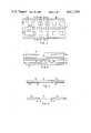
- FIG. 1is a plan view of a sheet of material illustrating the art work thereon for the manufacture of a metallic lead frame in accordance with the present invention
- FIG. 2illustrates a fragmentary portion of a transparent sheet having the art work thereon for superimposing the art work for one side of the metallic lead frame and the art work for the opposite side of the metallic lead frame;
- FIG. 3is a cross-sectional view of the sheets of material of FIG. 1 or 2 illustrating the art work applied to such sheets, and being separated to more clearly illustrate the registration of the art work;
- FIG. 4is a cross-sectional view of a metallic lead frame strip having the photoresist applied thereto and utilizing the superimposed art work of FIG. 3;
- FIG. 5is a cross-sectional view of a metallic strip that has been etched in accordance with the present invention.
- FIG. 6illustrates a typical bowed-out arrangement caused by lens distortion when photo reducing the art work for contact printing of a metallic lead frame on both sides thereof;
- FIG. 7illustrates the art work for both sides of a metallic lead frame superimposed to illustrate the registration of features in the manufacture of a metallic lead frame in accordance with the present invention
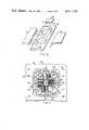
- FIG. 8is an enlarged fragmentary view of opposing leads of a metallic lead frame illustrating reference areas for the positioning of an integrated circuit chip in accordance with one embodiment of the present invention
- FIG. 9is a fragmentary plan view of a portion of a metallic lead frame and illustrates individual leads having a plurality of bonding bumps that are common to a given lead to register with pads on an integrated circuit chip which are electrically common to one another;
- FIG. 10is pictorial view of an FET chip together with its leads each whereby has a plurality of bonding bumps, said leads being shown spaced from the chips for clarity;
- FIG. 11is a fragmentary portion of a two-layer test frame that is configured to provide capability of testing a number of different-sized integrated circuit chips having various numbers of bonding pads;
- FIG. 12is a fragmentary view of the test strip of FIG. 13 illustrating the central opening that is enlarged to accommodate a chip of a size larger than could be accommodated with a central opening as illustrated in FIG. 11;
- FIG. 13is a diagrammatic sectional view of a metallic lead frame with a typical integrated circuit attached thereto that is bonded to a test frame strip such as shown in FIG. 11 or 12;
- FIG. 14illustrates a typical test set-up illustrating an IC chip being tested after the portion exterior of the bonded locations is removed.
- FIG. 15is a diagrammatic cross-sectional view illustrating a typical severing of the bonds of FIG. 14 after the tested chip has been removed to enlarge the central opening such as is shown in FIG. 11 or 12.
- metallic lead frames for semiconductor chipsare manufactured by spray etching from both sides, an elongated strip or tape of material, such as metal foil somewhat wider than the desired width, in order to form the leads, bonding bumps, tape edges, registration aids, part numbers, and sprocket holes.
- the individual lead framesare repeated at predetermined spaced intervals along the length of such tape with spaced registration or sprocket openings adjacent opposite side edges to engage with teeth in sprocket wheels of a conventional device for placing each lead frame in the proper position for bonding or other processing operations.
- the art work producing cyclebegins by taking the actual chip to be bonded and measuring the location of the bonding pads to produce a drawing on a 100 to 1 scale which, of course, provides extremely large art work spots that correspond to the actual photoresist bonding bump spots for the leads. This art work is then photographically reduced to 25 to 1 and the lead layout is then made at this scale.
- an enlarged art work image for both sides of a single-lead frame configurationis outlined on a transparent sheet of material, such as vinyl, for example, referred to at 31.
- the image for exposing the photoresist on one side of the metallic foil tapeis referred to at 32 and the image for exposing the photoresist for the same lead frame on the opposite side of the metallic foil strip is referred to at 32'.
- the art work for the sprocket openings of the metallic stripis referred to at 33 for one side thereof and the art work for the sprocket openings on the opposite side of the strip are referred to at 34.
- the images 32 and 32' as well as the sprocket opening images 33 and 34must be accurately aligned with respect to each other so that when the sheet material 31 is folded along a dashed line such as 35, for example, the sprocket opening images 33 and 34 and the art work images 32 and 32' will be in the proper registration for exposing the photoresist.
- the two imagesare photographically reduced to actual scale, or whatever scale is desired with respect to the required actual size of the individual lead frames of the strip; and then both images on the sheet are stepped and repeated together to generate a double string of images, such as shown in FIG. 2.
- the art work image 32 of a lead frame that exposes the photoresist on one side of the metallic stripmust register accurately with the art work image 32' that exposes the photoresist for the same lead frame on the opposite side of the strip.
- the spacing between successive sets of images after they have been stepped and repeatedneed not register to the same high degree of accuracy. Referring to FIG.
- a fragmentary portion of a length of an emulsified strip 36is shown that has been subjected to the step and repeat process and then developed to space the sprocket holes 33 and 34 and the images 32 and 32' in sequence along the length of such strip.
- any inaccuracies in the step and repeat mechanismis compensated for by the arrangement of the art work image as shown in FIG. 1 when applied to the emulsified strip 36.
- a distance referred to as 37must be the same as the distance referred to as 37' as shown in FIG. 2; and the distance referred to at 38 must be the same as the distance referred to at 38' in order to provide the proper registration of the images 32 and 32'.
- the distances 37 and 38may be different with respect to each other as may be caused by tolerances in a step and repeat mechanism.
- the upper image 32is superimposed on the lower image 32', by folding the strip 36 along a dashed line such as 40 for example, all of the images 32 and 32' along said strip are in proper registration with respect to each other.
- FIG. 3illustrates a metallic foil strip 41 interposed between emulsified surfaces 42 and 43 when the art work sheet 30 or 36 is folded on the dashed line such as 35 of FIG. 1 or 40 of FIG. 2, respectively.
- FIG. 4it is sufficient merely to mention that the conductive sheet 41 after being exposed to the photoresist is properly prepared for the etching process.
- FIG. 5illustrates the etched out portions of a section of the metallic piece 41 in accordance with the application of the photoresist.
- such a strip of imagesmay be photoreduced with a line of symmetry (40) of each pair of images 32 and 32' coinciding with the line of symmetry of a camera lens such that the reduced images though distorted is still symmetrical and therefore provides a series of superimposed images when cut and folded about its line of symmetry.
- the art work 32 for one side of the metallic lead frame strip referred to at 32includes a plurality of spaced leads referred to at 50 and a pair of spaced leads referred to at 51 and 52 respectively. It is understood, that the area within the continuous line 53 that forms the boundary and the individual leads of the frame is to be etched away during the etching process. Similarly, the openings 33 are also to be completely etched through the metallic lead frame strip.
- the art work image 32' which constitutes the pattern for exposing the photoresist to the opposite side of the metallic stripis comprised of a plurality of leads 54 which superimpose on the respective leads 50, 51 and 52 except that the leads 54 do not extend to the inner or free ends of the leads 50, 51 or 52.
- the image 32'also has a plurality of small spots 55 that correspond to the position of the bonding bumps at the inner or free end of the leads. Because of the extremely small size of the chip and the individual bonding pads thereon it is important that the bonding bumps align perfectly with its corresponding chip bonding pads even though such bonding bumps may be slightly offset at the end of its particular lead.
- an additional art work featuresuch as 56, for example, may be provided on the same art work 32' as that art work which locates the bumps 55.
- the outline of the chip which would be utilized with the completely etched metallic foil lead frameis shown at 57 and its inner edges such as 59. Art work 56 may correspond to the outline of the corners of such chip, for example.
- the additional features 56are on the same art work 32' as the art work which locates the bumps 55 and thus are always in the same registration with respect to each other even though the entire art work image 32' may not have perfect registration with the art work image 32.
- the additional registration features 56are shown as corresponding to the outline of the four corners of the chip, such art work may correspond to other recognizable features of the individual chip or include fewer corners.
- FIG. 7which shows the art work image 32 superimposed on the art work image 32', when folded along the line of symmetry 35, illustrates the registration of the two images as far out of alignment as is permissible; that is, the bumps 55 are still aligned with the ends of the leads 50, 51 and 52 but slightly displaced from center as shown therein. It will be noted that the features 56 shown in dotted lines of FIG. 7 are slightly displaced relative to the edges of the leads 50, 51 and 52 but are still accurately spaced with respect to the art work images 55 for the bonding bumps.
- the upper images 32'are severed from the lower images 32' as shown in the drawings along their respective lines 35 or 40, and placed in proper registration, emulsified surface 42 and 43 (FIG. 3) opposing each other to form an envelope, for example, or with the foil tape placed therebetween.
- the lead frame stripwhich previously has been coated with a photoresist and properly exposed as previously described, is ready for etching.
- itis preferably spray etched, but may be immersed in the etching solution a sufficient length of time so that those areas where the art work is absent on both sides of the strip are completely etched away; those particular areas in which the art work is present on only one side of such strip is etched approximately half of the thickness of the strip; and in the particular areas where the art work on the image 32 overlaps the art work on the image 32', the metallic foil retains its original thickness.
- FIG. 3is a cross-section of the emulsified strip 36, for example, showing superimposed the art work of FIG. 7, only shown slightly spaced from one another for clarity with the typical metallic strip 41 interposed;
- the art work 50which corresponds to the leads of the lead frame registers with the art work 55 that corresponds to the bonding bumps for the lead frame.
- the feature 56is illustrated to register with the lead frame 50 as more clearly shown in FIG. 7.
- the metallic lead frame cross-sectionis shown with those portions in dotted lines where no photoresist exists after development on the two sides and shown in solid lines where the photoresist 60 remains.
- FIG. 3is a cross-section of the emulsified strip 36, for example, showing superimposed the art work of FIG. 7, only shown slightly spaced from one another for clarity with the typical metallic strip 41 interposed;
- the art work 50which corresponds to the leads of the lead frame registers with the art work 55 that corresponds to the bonding bumps for the lead frame.
- the feature 56is illustrated to register
- a bonding bump 61is formed at the inner end of lead frame 62 and 63 respectively with the central portion 64 shown by the dashed lines being fully etched away.
- the additional features 67 for proper registration of the chip 57 where it overlaps the lead 62 and 63remains the full thickness of the metallic strip.
- the remaining portion of the lead of FIG. 5 exterior of the feature 56is full thickness where art work 50 and 54 overlapped to prevent exposure of the photoresist on the metallic lead frame.
- FIG. 8there is shown an enlarged plan view of a fragmentary portion of leads such as 62 and 63 to show the additional feature 67 (FIG. 5) integral therewith for registration with a chip, the outline of which is partially shown and referred to at 57.
- the degree of over etching or under etchingis not critical since the chip edges are centered between the registration features so as to produce a uniform gap at each corner of the chip.
- the bonding bumps 61(FIG. 5) cannot be seen from the top side when the chip is positioned for bonding in the central opening of the frame, the registration feature is viewable because it protrudes from beneath the individual leads and registers with the corners of the chip.
- the first of the pair of imagesdefines the set of leads which comprise a lead frame and the second of the pair defines the location of the bonding bumps at the inner or free ends of each of the leads. Additional registration features on the second of the pair which protrude away from the outline of the leads of the first of the pair and therefore are visible when viewed from the top side of the resulting metallic lead frame has been described.
- the additional art work featuresare made to register with some visible recognizable feature of the integrated circuit chip to which the bonding bumps of the metallic lead frame strip will ultimately be bonded.
- a strip of gang bonding lead frameswhich can be registered to integrated circuit chips has been provided without the need to be able to view the chip bonding pads or the lead bonding bumps.
- the raised soft metal bonding bumpsplastically deform when thermal compression bonding occurs. If the chip is exceeding small, and the bonding pads on the chip are very closely spaced such as is the case with a field effect transistor chip, it then becomes difficult to use the tape bonding process. It is not only difficult to produce the raised bumps on the bonding pads of the chips themselves, it is also difficult to etch very fine closely spaced lead frames with small integral bonding bumps on the free ends thereof. For example, where the fine lines of the lead frame are cantilevered for a long distance they also may bend so that the array of bonding bumps on the leads no longer register with the corresponding array of the bonding pads on the chip.
- a fragmentary portion of a metallic lead frame strip having integral raised bonding bumps 70 at the free or inner end of leads such as 71includes a lead 72 and a lead 73, both of which are much wider than the individual leads 71.
- the leads 72 and 73each have at their inner or free ends a plurality of spaced bonding bumps 74 and 75 respectively.
- the bonding bumps 74 and 75may be utilized to connect a number of bonding pads in common or to connect to a single bonding pad that would be to large for a lead having a single integral raised bonding bump at the end.
- a field effect transistor chip 76 having a row of electrically isolated drain pads 77, gate bonding pads 78, and source bonding areas 80may be successfully bonded to the lead frames having a structure in accordance with the present invention by providing the wide lead 72 with the spaced integral bonding bumps 74 each of which register with a respective drain pad 77 on the chip 76 so that the conductors have precisely the same impedance and thus does not permit the separate drains 77 to be out of phase with respect to one another, for example.
- a lead such as 81may be provided that has a plurality of bonding bumps 82 to register with the source bonding area 80, for example. This permits a bonding area which is too large to be bonded with a single large bump to provide the same ratio of bump height to bump width to provide adequate but not excessive bonding pressure on the bonding bumps to produce plastic deformation sufficient for a good thermal compression bond.
- the metallic foilmay be plated with a metal or metal alloy which is compatible with a chip bonding pad metallization, preferably gold, and fed into a conventional inner lead bonding machine.
- the lead framesuch as shown in FIG. 9 may be bonded to the chip by registering the bonding bumps over the bonding site of the chip and then compressing all of the bumps 74, 75 and 82 (not shown in FIG. 9) at elevated temperature. It is understood that the lead frame strip of FIG. 9 may be manufactured and have the additional features as previously described in FIGS. 1 through 8.
- the bonding bumpsmay be omitted on the above described lead frame tape simply by omitting the spots 55 on the art work.
- the tapecan be made with or without bumps.
- a two-layer test tape in accordance with the present inventionis referred to at 83 and comprises an insulative substrate 84 which is preferably polymide having sprocketing openings 85 therein; and on which is bonded a metallic pattern generally referred to as 86.
- the insulative tape 84 and the pattern 86has a central opening 87 which is shown as being rectangular in configuration to accommodate the chip to be tested.
- the outer perimeter of the pattern 86is formed by a plurality of metallic squares 88 spaced a predetermined distance apart and arranged in a rectangular configuration to form an outer boundary for the pattern and the central rectangular opening 87, the edges of which central opening 87 is referred to as the inner perimeter or boundary of the pattern 86.
- the particular metallic strips 90 that do not intersect the edge of the opening 87will, at a later time, intersect a larger square opening if such an opening were punched in the center of the pattern 86.
- Each one of the conductors 90is connected to a corresponding block 88 by a thin metallic strip such as 92. It is noted that inwardly of the pads 88 to which the test probes are placed in contact for testing an integrated circuit, are a plurality of rectangular metallic pads 88'. These pads are merely to provide a symmetrical arrangement for engaging a test probe without increasing the overall perimeter of the outer boundary of the pads 88.
- a dashed line 95 of FIG. 11outlines the manner in which the opening 87 could be enlarged to accommodate a larger size chip than could be accommodated by the opening 87 as shown in FIG. 11 and at the same time provide additional metallic leads 90 that would abut the edge of the opening.
- the metallic leads 90are preferably copper plated with an electrodeless tin.
- the test frame 83is identical to the test frame shown and described in connection with FIG. 11 except that the opening 87 has been enlarged to its maximum extent such that all of the spaced conductors 90 abut a corresponding edge of the opening 87.
- the test tape inner boundary or opening 87is shown to approximately its maximum enlargement, it is understood that the opening 87 may be enlarged for each testing operation in intermediate increments.
- the double-layer test tape 83may be utilized a number of times, first in connection with testing a small size chip and then successively a larger sized chip with additional leads as described.
- the metallic lead frame that is designed for a particular chipis first bonded via its integral bonding bumps at the end of its leads to the corresponding bonding pads on the chip by compression bonding.
- the lead frame tape(FIG. 9) with the bonded chip (not shown) is then bonded to the conductive lines 90. Since the conductors of the test tape are tin-plated and the lead frame is gold-plated, a gold/tin solder joint is formed between the two copper foils.
- the chipcannot be tested because it is evident that all of the leads are shorted together because of the solid metallic foil lead frame strip.
- Such lead frame stripof course must provide for a specific dimensional relationship of each individual frame to its sprocket openings.
- the excess gold-plated foilis removed leaving the chip bonded to the test tape for testing.
- the sprocket holes of the single layer tapesuch as shown in FIG. 9 are made to register with the sprocket holes of the two layer test tape as shown in FIGS. 11 and 12; and the leads of the lead frame register with predetermined metallic strips 90 on the two-layer insulation tape.
- the number of bonding pads on the chip to be bondedmay be less than or equal to the number of available conductive strips 90 on the test tape 83. To make the most effective use of the test tape, it should first be used with the smaller sized chips with fewer bonding pads so that it can be reused for larger sized chips with more bonding pads by merely punching the hole 87 a larger size.
- FIG. 13a diagrammatic cross-sectional view of a fixture 100 is shown with the test tape 83 having the insulative substrate 84 and showing a metallic strip 90 positioned with the metallic lead frame tape 69 overlying the same such that a chip 101 is spaced so that the central opening 87 of this test tape and a recessed portion 102 are in registration.
- the individual leads 71are then bonded at 103 adjacent the edge of the central opening 87 of the test tape to form a compression bond such as a gold/tin soldered joint.
- This bondingmay be any conventional bonding operation but preferably is the formation of a eutectic alloy between different surface metallizations applied to the strips 90 and the leads 71.
- the metallic strip 69is lifted and removed from the test tape where it severes at the outer end of each of the leads.
- This severing of the individual leads of the lead frameoccurs in a ready manner due to the formation of the base end of ech of the individual leads.
- the space between each of the individual leadsis configured so that the lead itself fans out at its base to provide a greater strength adjacent such base end so that the weak point 76 of each of the leads 71 is at the outer end of the lead frame.
- the double-layer test tape 83 with severed leads bonded thereto as previously describedis shown in position for testing.
- a conventional test fixture 105is connected through a coupling 106 to individual probes 107 on a fixture 108 to engage the appropriate individual metallic pads 88 and 88' of FIGS. 11 and 12.
- the chipsOnce the chips have been tested, they may be severed in a conventional manner such as at 99 adjacent the peripheral edge of the central opening 87 of the test tape. This of course, leaves the bond between the outer portion of the individual leads of the lead frame still bonded adjacent the peripheral opening 87 to the metallic portion 90 of the test tape 83.
- such bonded portionmay be severed adjacent its exterior surface by a conventional punch 110 which is of similar configuration to the central opening 87 but slightly larger sufficient to at least remove the alloy formation 103.
- the portion of the test tape referred to at 111 within the rectangular punch 110is then discarded and the remaining portion of the test tape having a slightly larger central opening may be reused.
- a larger chipmay be bonded at its free end to a custom lead frame having leads capable of registering with the metallic strips 90 of the tape and the procedure repeated. This procedure can continue for successively larger size chips with a larger number of leads until the central opening is made to its maximum size such as shown in FIG. 12.
- the opening 87may be enlarged sufficiently to expose two additional strips 90 for each incrementally larger size chip to be tested. With predetermined incremental enlargements, standardization of various sizes of chips to be tested can be effected.
- the test fixture described in connection with FIG. 14may have one contact probe for each of the pads 88, 88' even though many of the pads may not be connected to anything on the chip.
- the contact probes 107 of FIG. 14 and the connector portion 106'could be utilized for all of the different chips to be tested; that is, it could be set up originally to provide the proper contact for the pads 88 or 88' of the universal two layer test tape in accordance with the present invention.
- the mating connector 106 and the test device 105of course would be different for each different chip.
- the conductive pattern 86is made up of a large number of conductive lines 90 which extend toward the edge of the centrally spaced hole such as 87 and which connects to large probe pads such as 88 or 88' spaced away and exterior of the center clearance hole 87.
- the conductive linesterminate at the edge of the central opening 87 regardless of its size in the central portion of the insulative strip 84.
- the integrated circuit chipsare testable after being bonded to the metallic lead frame strip by bonding the leads to the metallic strips as hereinbefore described by thermo-compression bonding; and the lead frame strip is removed and separated from the leads.
- none of the metal that bonds the outer ends of each of the leads of the lead framepermanently remains with the chip and may therefore be metallized with a non-noble metallization in order to achieve moderate temperature eutectic alloy formation when the bonding of the leads to the test tape is accomplished.
- the conductive pattern of the universal test tape in accordance with the present inventionmay also be probed by the same probing pins during the testing operation regardless of the integrated circuit chip being tested.
Landscapes
- Engineering & Computer Science (AREA)
- Computer Hardware Design (AREA)
- Microelectronics & Electronic Packaging (AREA)
- Power Engineering (AREA)
- Manufacturing & Machinery (AREA)
- Physics & Mathematics (AREA)
- General Physics & Mathematics (AREA)
- Condensed Matter Physics & Semiconductors (AREA)
- General Engineering & Computer Science (AREA)
- Wire Bonding (AREA)
Abstract
Description
Claims (8)
Priority Applications (1)
| Application Number | Priority Date | Filing Date | Title |
|---|---|---|---|
| US06/263,962US4411719A (en) | 1980-02-07 | 1981-05-14 | Apparatus and method for tape bonding and testing of integrated circuit chips |
Applications Claiming Priority (2)
| Application Number | Priority Date | Filing Date | Title |
|---|---|---|---|
| US06/119,247US4308339A (en) | 1980-02-07 | 1980-02-07 | Method for manufacturing tape including lead frames |
| US06/263,962US4411719A (en) | 1980-02-07 | 1981-05-14 | Apparatus and method for tape bonding and testing of integrated circuit chips |
Related Parent Applications (1)
| Application Number | Title | Priority Date | Filing Date |
|---|---|---|---|
| US06/119,247DivisionUS4308339A (en) | 1980-02-07 | 1980-02-07 | Method for manufacturing tape including lead frames |
Publications (1)
| Publication Number | Publication Date |
|---|---|
| US4411719Atrue US4411719A (en) | 1983-10-25 |
Family
ID=26817160
Family Applications (1)
| Application Number | Title | Priority Date | Filing Date |
|---|---|---|---|
| US06/263,962Expired - LifetimeUS4411719A (en) | 1980-02-07 | 1981-05-14 | Apparatus and method for tape bonding and testing of integrated circuit chips |
Country Status (1)
| Country | Link |
|---|---|
| US (1) | US4411719A (en) |
Cited By (65)
| Publication number | Priority date | Publication date | Assignee | Title |
|---|---|---|---|---|
| US4538210A (en)* | 1982-04-15 | 1985-08-27 | Siemens Aktiengesellschaft | Mounting and contacting assembly for plate-shaped electrical device |
| US4549194A (en)* | 1982-03-29 | 1985-10-22 | Eaton Corporation | Light sensitive detector |
| EP0175995A1 (en)* | 1984-09-21 | 1986-04-02 | Siemens Aktiengesellschaft | Arrangement for testing integrated circuits |
| WO1987005153A1 (en)* | 1986-02-20 | 1987-08-27 | Aegis, Inc. | Lead frame having non-conductive tie-bar for use in integrated circuit packages |
| US4701363A (en)* | 1986-01-27 | 1987-10-20 | Olin Corporation | Process for manufacturing bumped tape for tape automated bonding and the product produced thereby |
| US4735678A (en)* | 1987-04-13 | 1988-04-05 | Olin Corporation | Forming a circuit pattern in a metallic tape by electrical discharge machining |
| US4763409A (en)* | 1985-08-23 | 1988-08-16 | Nec Corporation | Method of manufacturing semiconductor device |
| US4799128A (en)* | 1985-12-20 | 1989-01-17 | Ncr Corporation | Multilayer printed circuit board with domain partitioning |
| US4855672A (en)* | 1987-05-18 | 1989-08-08 | Shreeve Robert W | Method and process for testing the reliability of integrated circuit (IC) chips and novel IC circuitry for accomplishing same |
| US4967260A (en)* | 1988-05-04 | 1990-10-30 | International Electronic Research Corp. | Hermetic microminiature packages |
| US4969828A (en)* | 1989-05-17 | 1990-11-13 | Amp Incorporated | Electrical socket for TAB IC's |
| US4980034A (en)* | 1989-04-04 | 1990-12-25 | Massachusetts Institute Of Technology | High-density, multi-level interconnects, flex circuits, and tape for TAB |
| US4981817A (en)* | 1988-12-29 | 1991-01-01 | International Business Machines Corporation | Tab method for implementing dynamic chip burn-in |
| EP0408101A2 (en)* | 1989-07-14 | 1991-01-16 | Lsi Logic Corporation | Strip carrier for integrated circuits |
| US5002895A (en)* | 1987-04-17 | 1991-03-26 | Thomson-Csf | Wire bonding method with a frame, for connecting an electronic component for testing and mounting |
| DE4017863C1 (en)* | 1990-06-02 | 1991-07-18 | Du Pont De Nemours (Deutschland) Gmbh, 4000 Duesseldorf, De | |
| US5036380A (en)* | 1988-03-28 | 1991-07-30 | Digital Equipment Corp. | Burn-in pads for tab interconnects |
| US5053357A (en)* | 1989-12-27 | 1991-10-01 | Motorola, Inc. | Method of aligning and mounting an electronic device on a printed circuit board using a flexible substrate having fixed lead arrays thereon |
| US5086271A (en)* | 1990-01-12 | 1992-02-04 | Reliability Incorporated | Driver system and distributed transmission line network for driving devices under test |
| US5106461A (en)* | 1989-04-04 | 1992-04-21 | Massachusetts Institute Of Technology | High-density, multi-level interconnects, flex circuits, and tape for tab |
| US5157476A (en)* | 1990-03-12 | 1992-10-20 | Kabushiki Kaisha Toshiba | Tape carrier having improved test pads |
| US5285105A (en)* | 1988-12-07 | 1994-02-08 | Tribotech | Semiconductor die packages having lead support frame |
| US5308443A (en)* | 1989-11-30 | 1994-05-03 | Hoya Corporation | Microprobe provided circuit substrate and method for producing the same |
| US5491891A (en)* | 1993-03-25 | 1996-02-20 | Probes Associates, Inc. | Method of making a test probe ring |
| US5677203A (en)* | 1993-12-15 | 1997-10-14 | Chip Supply, Inc. | Method for providing known good bare semiconductor die |
| EP0845680A1 (en)* | 1990-02-16 | 1998-06-03 | LEEDY, Glenn J. | Making and testing an integrated circuit using high density probe points |
| US5763294A (en)* | 1997-05-15 | 1998-06-09 | Compeq Manufacturing Company Limited | Solid tape automated bonding packaging method |
| US5766978A (en)* | 1996-01-26 | 1998-06-16 | Hewlett-Packard Company | Process for testing an integrated circuit package using an integrated circuit package retainer |
| US5854094A (en)* | 1992-07-28 | 1998-12-29 | Shinko Electric Industries Co., Ltd. | Process for manufacturing metal plane support for multi-layer lead frames |
| US6372526B1 (en)* | 1998-04-06 | 2002-04-16 | Semiconductor Components Industries Llc | Method of manufacturing semiconductor components |
| US6429050B1 (en)* | 1997-12-18 | 2002-08-06 | Texas Instruments Incorporated | Fine pitch lead frame and method |
| US20050133898A1 (en)* | 2003-12-22 | 2005-06-23 | Brother Kogyo Kabushiki Kaisha | Printed circuit board and inkjet head |
| US20080128159A1 (en)* | 2003-12-19 | 2008-06-05 | Brother Kogyo Kabushiki Kaisha | Method for manufacturing a printed circuit board that mounts an integrated circuit device thereon and the printed circuit board |
| US20080188015A1 (en)* | 2006-04-27 | 2008-08-07 | Saruch Sangaunwong | Testing and burn-in using a strip socket |
| US20080197507A1 (en)* | 2007-02-16 | 2008-08-21 | Yu-Lin Yang | Electronic package structure and method |
| US20090209064A1 (en)* | 2006-04-28 | 2009-08-20 | Somchai Nonahasitthichai | Lead frame land grid array |
| US7632373B2 (en) | 2004-09-03 | 2009-12-15 | Tyco Electronics Corporation | Method of making electrical devices having an oxygen barrier coating |
| US7790512B1 (en) | 2007-11-06 | 2010-09-07 | Utac Thai Limited | Molded leadframe substrate semiconductor package |
| US20100233854A1 (en)* | 2009-03-12 | 2010-09-16 | Utac Thai Limited | Metallic solderability preservation coating on metal part of semiconductor package to prevent oxide |
| US20100327432A1 (en)* | 2006-09-26 | 2010-12-30 | Utac Thai Limited | Package with heat transfer |
| US20110018111A1 (en)* | 2009-07-23 | 2011-01-27 | Utac Thai Limited | Leadframe feature to minimize flip-chip semiconductor die collapse during flip-chip reflow |
| US20110039371A1 (en)* | 2008-09-04 | 2011-02-17 | Utac Thai Limited | Flip chip cavity package |
| US20110089968A1 (en)* | 2009-10-19 | 2011-04-21 | Advantest Corporation | Electronic device mounting apparatus and method of mounting electronic device |
| US20110147931A1 (en)* | 2006-04-28 | 2011-06-23 | Utac Thai Limited | Lead frame land grid array with routing connector trace under unit |
| US8013437B1 (en) | 2006-09-26 | 2011-09-06 | Utac Thai Limited | Package with heat transfer |
| US20110221051A1 (en)* | 2010-03-11 | 2011-09-15 | Utac Thai Limited | Leadframe based multi terminal ic package |
| US8063470B1 (en) | 2008-05-22 | 2011-11-22 | Utac Thai Limited | Method and apparatus for no lead semiconductor package |
| US8334764B1 (en) | 2008-12-17 | 2012-12-18 | Utac Thai Limited | Method and apparatus to prevent double semiconductor units in test socket |
| US8368189B2 (en) | 2009-12-04 | 2013-02-05 | Utac Thai Limited | Auxiliary leadframe member for stabilizing the bond wire process |
| US8461694B1 (en) | 2006-04-28 | 2013-06-11 | Utac Thai Limited | Lead frame ball grid array with traces under die having interlocking features |
| US8460970B1 (en) | 2006-04-28 | 2013-06-11 | Utac Thai Limited | Lead frame ball grid array with traces under die having interlocking features |
| US8492906B2 (en) | 2006-04-28 | 2013-07-23 | Utac Thai Limited | Lead frame ball grid array with traces under die |
| US8871571B2 (en) | 2010-04-02 | 2014-10-28 | Utac Thai Limited | Apparatus for and methods of attaching heat slugs to package tops |
| US9000590B2 (en) | 2012-05-10 | 2015-04-07 | Utac Thai Limited | Protruding terminals with internal routing interconnections semiconductor device |
| US9006034B1 (en) | 2012-06-11 | 2015-04-14 | Utac Thai Limited | Post-mold for semiconductor package having exposed traces |
| US9082607B1 (en) | 2006-12-14 | 2015-07-14 | Utac Thai Limited | Molded leadframe substrate semiconductor package |
| US9355940B1 (en) | 2009-12-04 | 2016-05-31 | Utac Thai Limited | Auxiliary leadframe member for stabilizing the bond wire process |
| US9449905B2 (en) | 2012-05-10 | 2016-09-20 | Utac Thai Limited | Plated terminals with routing interconnections semiconductor device |
| US9761435B1 (en) | 2006-12-14 | 2017-09-12 | Utac Thai Limited | Flip chip cavity package |
| US9805955B1 (en) | 2015-11-10 | 2017-10-31 | UTAC Headquarters Pte. Ltd. | Semiconductor package with multiple molding routing layers and a method of manufacturing the same |
| US10242953B1 (en) | 2015-05-27 | 2019-03-26 | Utac Headquarters PTE. Ltd | Semiconductor package with plated metal shielding and a method thereof |
| US10242934B1 (en) | 2014-05-07 | 2019-03-26 | Utac Headquarters Pte Ltd. | Semiconductor package with full plating on contact side surfaces and methods thereof |
| US10276477B1 (en) | 2016-05-20 | 2019-04-30 | UTAC Headquarters Pte. Ltd. | Semiconductor package with multiple stacked leadframes and a method of manufacturing the same |
| CN111766409A (en)* | 2019-04-02 | 2020-10-13 | 精英电脑股份有限公司 | Device and method for instant positioning of panel components |
| US20230215786A1 (en)* | 2021-12-30 | 2023-07-06 | Harvatek Corporation | Planar multi-chip device |
Citations (5)
| Publication number | Priority date | Publication date | Assignee | Title |
|---|---|---|---|---|
| US3440027A (en)* | 1966-06-22 | 1969-04-22 | Frances Hugle | Automated packaging of semiconductors |
| US3678385A (en)* | 1969-09-26 | 1972-07-18 | Amp Inc | Assembly and test device for microelectronic circuit members |
| US3777365A (en)* | 1972-03-06 | 1973-12-11 | Honeywell Inf Systems | Circuit chips having beam leads attached by film strip process |
| US3781596A (en)* | 1972-07-07 | 1973-12-25 | R Galli | Semiconductor chip carriers and strips thereof |
| US4220917A (en)* | 1978-07-31 | 1980-09-02 | International Business Machines Corporation | Test circuitry for module interconnection network |
- 1981
- 1981-05-14USUS06/263,962patent/US4411719A/ennot_activeExpired - Lifetime
Patent Citations (5)
| Publication number | Priority date | Publication date | Assignee | Title |
|---|---|---|---|---|
| US3440027A (en)* | 1966-06-22 | 1969-04-22 | Frances Hugle | Automated packaging of semiconductors |
| US3678385A (en)* | 1969-09-26 | 1972-07-18 | Amp Inc | Assembly and test device for microelectronic circuit members |
| US3777365A (en)* | 1972-03-06 | 1973-12-11 | Honeywell Inf Systems | Circuit chips having beam leads attached by film strip process |
| US3781596A (en)* | 1972-07-07 | 1973-12-25 | R Galli | Semiconductor chip carriers and strips thereof |
| US4220917A (en)* | 1978-07-31 | 1980-09-02 | International Business Machines Corporation | Test circuitry for module interconnection network |
Cited By (115)
| Publication number | Priority date | Publication date | Assignee | Title |
|---|---|---|---|---|
| US4549194A (en)* | 1982-03-29 | 1985-10-22 | Eaton Corporation | Light sensitive detector |
| US4538210A (en)* | 1982-04-15 | 1985-08-27 | Siemens Aktiengesellschaft | Mounting and contacting assembly for plate-shaped electrical device |
| EP0175995A1 (en)* | 1984-09-21 | 1986-04-02 | Siemens Aktiengesellschaft | Arrangement for testing integrated circuits |
| US4868493A (en)* | 1984-09-21 | 1989-09-19 | Siemens Aktiengesellschaft | Device for the functional testing of integrated circuits and a method for operating the device |
| US4763409A (en)* | 1985-08-23 | 1988-08-16 | Nec Corporation | Method of manufacturing semiconductor device |
| US4799128A (en)* | 1985-12-20 | 1989-01-17 | Ncr Corporation | Multilayer printed circuit board with domain partitioning |
| US4701363A (en)* | 1986-01-27 | 1987-10-20 | Olin Corporation | Process for manufacturing bumped tape for tape automated bonding and the product produced thereby |
| WO1987005153A1 (en)* | 1986-02-20 | 1987-08-27 | Aegis, Inc. | Lead frame having non-conductive tie-bar for use in integrated circuit packages |
| US4768077A (en)* | 1986-02-20 | 1988-08-30 | Aegis, Inc. | Lead frame having non-conductive tie-bar for use in integrated circuit packages |
| US4735678A (en)* | 1987-04-13 | 1988-04-05 | Olin Corporation | Forming a circuit pattern in a metallic tape by electrical discharge machining |
| US5002895A (en)* | 1987-04-17 | 1991-03-26 | Thomson-Csf | Wire bonding method with a frame, for connecting an electronic component for testing and mounting |
| US4855672A (en)* | 1987-05-18 | 1989-08-08 | Shreeve Robert W | Method and process for testing the reliability of integrated circuit (IC) chips and novel IC circuitry for accomplishing same |
| US5036380A (en)* | 1988-03-28 | 1991-07-30 | Digital Equipment Corp. | Burn-in pads for tab interconnects |
| US4967260A (en)* | 1988-05-04 | 1990-10-30 | International Electronic Research Corp. | Hermetic microminiature packages |
| US5285105A (en)* | 1988-12-07 | 1994-02-08 | Tribotech | Semiconductor die packages having lead support frame |
| US4981817A (en)* | 1988-12-29 | 1991-01-01 | International Business Machines Corporation | Tab method for implementing dynamic chip burn-in |
| US4980034A (en)* | 1989-04-04 | 1990-12-25 | Massachusetts Institute Of Technology | High-density, multi-level interconnects, flex circuits, and tape for TAB |
| US5106461A (en)* | 1989-04-04 | 1992-04-21 | Massachusetts Institute Of Technology | High-density, multi-level interconnects, flex circuits, and tape for tab |
| US4969828A (en)* | 1989-05-17 | 1990-11-13 | Amp Incorporated | Electrical socket for TAB IC's |
| US5023202A (en)* | 1989-07-14 | 1991-06-11 | Lsi Logic Corporation | Rigid strip carrier for integrated circuits |
| EP0408101A2 (en)* | 1989-07-14 | 1991-01-16 | Lsi Logic Corporation | Strip carrier for integrated circuits |
| US5308443A (en)* | 1989-11-30 | 1994-05-03 | Hoya Corporation | Microprobe provided circuit substrate and method for producing the same |
| US5053357A (en)* | 1989-12-27 | 1991-10-01 | Motorola, Inc. | Method of aligning and mounting an electronic device on a printed circuit board using a flexible substrate having fixed lead arrays thereon |
| US5086271A (en)* | 1990-01-12 | 1992-02-04 | Reliability Incorporated | Driver system and distributed transmission line network for driving devices under test |
| EP0845680A1 (en)* | 1990-02-16 | 1998-06-03 | LEEDY, Glenn J. | Making and testing an integrated circuit using high density probe points |
| US5157476A (en)* | 1990-03-12 | 1992-10-20 | Kabushiki Kaisha Toshiba | Tape carrier having improved test pads |
| DE4017863C1 (en)* | 1990-06-02 | 1991-07-18 | Du Pont De Nemours (Deutschland) Gmbh, 4000 Duesseldorf, De | |
| US5210006A (en)* | 1990-06-02 | 1993-05-11 | E. I. Du Pont De Nemours And Company | Process for preparing mounting tapes for automatic mounting of electronic components |
| US5854094A (en)* | 1992-07-28 | 1998-12-29 | Shinko Electric Industries Co., Ltd. | Process for manufacturing metal plane support for multi-layer lead frames |
| US5491891A (en)* | 1993-03-25 | 1996-02-20 | Probes Associates, Inc. | Method of making a test probe ring |
| US5677203A (en)* | 1993-12-15 | 1997-10-14 | Chip Supply, Inc. | Method for providing known good bare semiconductor die |
| US5766978A (en)* | 1996-01-26 | 1998-06-16 | Hewlett-Packard Company | Process for testing an integrated circuit package using an integrated circuit package retainer |
| US5763294A (en)* | 1997-05-15 | 1998-06-09 | Compeq Manufacturing Company Limited | Solid tape automated bonding packaging method |
| US6429050B1 (en)* | 1997-12-18 | 2002-08-06 | Texas Instruments Incorporated | Fine pitch lead frame and method |
| US6724070B2 (en) | 1997-12-18 | 2004-04-20 | Texas Instruments Incorporated | Fine pitch lead frame |
| US6372526B1 (en)* | 1998-04-06 | 2002-04-16 | Semiconductor Components Industries Llc | Method of manufacturing semiconductor components |
| US20080128159A1 (en)* | 2003-12-19 | 2008-06-05 | Brother Kogyo Kabushiki Kaisha | Method for manufacturing a printed circuit board that mounts an integrated circuit device thereon and the printed circuit board |
| US20050133898A1 (en)* | 2003-12-22 | 2005-06-23 | Brother Kogyo Kabushiki Kaisha | Printed circuit board and inkjet head |
| EP1548826A1 (en) | 2003-12-22 | 2005-06-29 | Brother Kogyo Kabushiki Kaisha | Chip pad layout |
| US7271478B2 (en) | 2003-12-22 | 2007-09-18 | Brother Kogyo Kabushiki Kaisha | Printed circuit board and inkjet head |
| US7632373B2 (en) | 2004-09-03 | 2009-12-15 | Tyco Electronics Corporation | Method of making electrical devices having an oxygen barrier coating |
| US7656173B1 (en)* | 2006-04-27 | 2010-02-02 | Utac Thai Limited | Strip socket having a recessed portions in the base to accept bottom surface of packaged semiconductor devices mounted on a leadframe for testing and burn-in |
| US20080211072A1 (en)* | 2006-04-27 | 2008-09-04 | Saruch Sangaunwong | Testing and burn-in using a strip socket |
| US7696772B2 (en) | 2006-04-27 | 2010-04-13 | Ns Electronics Bangkok Ltd | Strip socket for testing and burn-in having recessed portions with material that extends across a bottom surface of the corresponding semiconductor device |
| US20080188015A1 (en)* | 2006-04-27 | 2008-08-07 | Saruch Sangaunwong | Testing and burn-in using a strip socket |
| US8685794B2 (en) | 2006-04-28 | 2014-04-01 | Utac Thai Limited | Lead frame land grid array with routing connector trace under unit |
| US20090209064A1 (en)* | 2006-04-28 | 2009-08-20 | Somchai Nonahasitthichai | Lead frame land grid array |
| US8704381B2 (en) | 2006-04-28 | 2014-04-22 | Utac Thai Limited | Very extremely thin semiconductor package |
| US20100127363A1 (en)* | 2006-04-28 | 2010-05-27 | Utac Thai Limited | Very extremely thin semiconductor package |
| US9099317B2 (en) | 2006-04-28 | 2015-08-04 | Utac Thai Limited | Method for forming lead frame land grid array |
| US8652879B2 (en) | 2006-04-28 | 2014-02-18 | Utac Thai Limited | Lead frame ball grid array with traces under die |
| US8575762B2 (en) | 2006-04-28 | 2013-11-05 | Utac Thai Limited | Very extremely thin semiconductor package |
| US8492906B2 (en) | 2006-04-28 | 2013-07-23 | Utac Thai Limited | Lead frame ball grid array with traces under die |
| US8487451B2 (en) | 2006-04-28 | 2013-07-16 | Utac Thai Limited | Lead frame land grid array with routing connector trace under unit |
| US8460970B1 (en) | 2006-04-28 | 2013-06-11 | Utac Thai Limited | Lead frame ball grid array with traces under die having interlocking features |
| US8461694B1 (en) | 2006-04-28 | 2013-06-11 | Utac Thai Limited | Lead frame ball grid array with traces under die having interlocking features |
| US20110147931A1 (en)* | 2006-04-28 | 2011-06-23 | Utac Thai Limited | Lead frame land grid array with routing connector trace under unit |
| US8310060B1 (en) | 2006-04-28 | 2012-11-13 | Utac Thai Limited | Lead frame land grid array |
| US8013437B1 (en) | 2006-09-26 | 2011-09-06 | Utac Thai Limited | Package with heat transfer |
| US8125077B2 (en) | 2006-09-26 | 2012-02-28 | Utac Thai Limited | Package with heat transfer |
| US20100327432A1 (en)* | 2006-09-26 | 2010-12-30 | Utac Thai Limited | Package with heat transfer |
| US9099294B1 (en) | 2006-12-14 | 2015-08-04 | Utac Thai Limited | Molded leadframe substrate semiconductor package |
| US9082607B1 (en) | 2006-12-14 | 2015-07-14 | Utac Thai Limited | Molded leadframe substrate semiconductor package |
| US9093486B2 (en) | 2006-12-14 | 2015-07-28 | Utac Thai Limited | Molded leadframe substrate semiconductor package |
| US9899208B2 (en) | 2006-12-14 | 2018-02-20 | Utac Thai Limited | Molded leadframe substrate semiconductor package |
| US9761435B1 (en) | 2006-12-14 | 2017-09-12 | Utac Thai Limited | Flip chip cavity package |
| US9711343B1 (en) | 2006-12-14 | 2017-07-18 | Utac Thai Limited | Molded leadframe substrate semiconductor package |
| US9196470B1 (en) | 2006-12-14 | 2015-11-24 | Utac Thai Limited | Molded leadframe substrate semiconductor package |
| US20080197507A1 (en)* | 2007-02-16 | 2008-08-21 | Yu-Lin Yang | Electronic package structure and method |
| US20100124801A1 (en)* | 2007-02-16 | 2010-05-20 | Richtek Technology Corp. | Electronic package structure and method |
| US8338922B1 (en) | 2007-11-06 | 2012-12-25 | Utac Thai Limited | Molded leadframe substrate semiconductor package |
| US7790512B1 (en) | 2007-11-06 | 2010-09-07 | Utac Thai Limited | Molded leadframe substrate semiconductor package |
| US8063470B1 (en) | 2008-05-22 | 2011-11-22 | Utac Thai Limited | Method and apparatus for no lead semiconductor package |
| US8071426B2 (en) | 2008-05-22 | 2011-12-06 | Utac Thai Limited | Method and apparatus for no lead semiconductor package |
| US20110039371A1 (en)* | 2008-09-04 | 2011-02-17 | Utac Thai Limited | Flip chip cavity package |
| US9947605B2 (en) | 2008-09-04 | 2018-04-17 | UTAC Headquarters Pte. Ltd. | Flip chip cavity package |
| US8334764B1 (en) | 2008-12-17 | 2012-12-18 | Utac Thai Limited | Method and apparatus to prevent double semiconductor units in test socket |
| US8569877B2 (en) | 2009-03-12 | 2013-10-29 | Utac Thai Limited | Metallic solderability preservation coating on metal part of semiconductor package to prevent oxide |
| US20110232693A1 (en)* | 2009-03-12 | 2011-09-29 | Utac Thai Limited | Metallic solderability preservation coating on metal part of semiconductor package to prevent oxide |
| US20100233854A1 (en)* | 2009-03-12 | 2010-09-16 | Utac Thai Limited | Metallic solderability preservation coating on metal part of semiconductor package to prevent oxide |
| US8367476B2 (en) | 2009-03-12 | 2013-02-05 | Utac Thai Limited | Metallic solderability preservation coating on metal part of semiconductor package to prevent oxide |
| US8431443B2 (en) | 2009-03-12 | 2013-04-30 | Utac Thai Limited | Metallic solderability preservation coating on metal part of semiconductor package to prevent oxide |
| US20100230802A1 (en)* | 2009-03-12 | 2010-09-16 | Utac Thai Limited | Metallic solderability preservation coating on metal part of semiconductor package to prevent oxide |
| US9449900B2 (en) | 2009-07-23 | 2016-09-20 | UTAC Headquarters Pte. Ltd. | Leadframe feature to minimize flip-chip semiconductor die collapse during flip-chip reflow |
| US20110018111A1 (en)* | 2009-07-23 | 2011-01-27 | Utac Thai Limited | Leadframe feature to minimize flip-chip semiconductor die collapse during flip-chip reflow |
| US8653846B2 (en)* | 2009-10-19 | 2014-02-18 | Advantest Corporation | Electronic device mounting apparatus and method of mounting electronic device |
| US20110089968A1 (en)* | 2009-10-19 | 2011-04-21 | Advantest Corporation | Electronic device mounting apparatus and method of mounting electronic device |
| US9355940B1 (en) | 2009-12-04 | 2016-05-31 | Utac Thai Limited | Auxiliary leadframe member for stabilizing the bond wire process |
| US8368189B2 (en) | 2009-12-04 | 2013-02-05 | Utac Thai Limited | Auxiliary leadframe member for stabilizing the bond wire process |
| US20110221051A1 (en)* | 2010-03-11 | 2011-09-15 | Utac Thai Limited | Leadframe based multi terminal ic package |
| US8575732B2 (en) | 2010-03-11 | 2013-11-05 | Utac Thai Limited | Leadframe based multi terminal IC package |
| US8722461B2 (en) | 2010-03-11 | 2014-05-13 | Utac Thai Limited | Leadframe based multi terminal IC package |
| US8871571B2 (en) | 2010-04-02 | 2014-10-28 | Utac Thai Limited | Apparatus for and methods of attaching heat slugs to package tops |
| US9922913B2 (en) | 2012-05-10 | 2018-03-20 | Utac Thai Limited | Plated terminals with routing interconnections semiconductor device |
| US9000590B2 (en) | 2012-05-10 | 2015-04-07 | Utac Thai Limited | Protruding terminals with internal routing interconnections semiconductor device |
| US9449905B2 (en) | 2012-05-10 | 2016-09-20 | Utac Thai Limited | Plated terminals with routing interconnections semiconductor device |
| US9922914B2 (en) | 2012-05-10 | 2018-03-20 | Utac Thai Limited | Plated terminals with routing interconnections semiconductor device |
| US9029198B2 (en) | 2012-05-10 | 2015-05-12 | Utac Thai Limited | Methods of manufacturing semiconductor devices including terminals with internal routing interconnections |
| US9972563B2 (en) | 2012-05-10 | 2018-05-15 | UTAC Headquarters Pte. Ltd. | Plated terminals with routing interconnections semiconductor device |
| US9006034B1 (en) | 2012-06-11 | 2015-04-14 | Utac Thai Limited | Post-mold for semiconductor package having exposed traces |
| US9397031B2 (en) | 2012-06-11 | 2016-07-19 | Utac Thai Limited | Post-mold for semiconductor package having exposed traces |
| US10242934B1 (en) | 2014-05-07 | 2019-03-26 | Utac Headquarters Pte Ltd. | Semiconductor package with full plating on contact side surfaces and methods thereof |
| US10269686B1 (en) | 2015-05-27 | 2019-04-23 | UTAC Headquarters PTE, LTD. | Method of improving adhesion between molding compounds and an apparatus thereof |
| US10242953B1 (en) | 2015-05-27 | 2019-03-26 | Utac Headquarters PTE. Ltd | Semiconductor package with plated metal shielding and a method thereof |
| US9805955B1 (en) | 2015-11-10 | 2017-10-31 | UTAC Headquarters Pte. Ltd. | Semiconductor package with multiple molding routing layers and a method of manufacturing the same |
| US10096490B2 (en) | 2015-11-10 | 2018-10-09 | UTAC Headquarters Pte. Ltd. | Semiconductor package with multiple molding routing layers and a method of manufacturing the same |
| US10163658B2 (en) | 2015-11-10 | 2018-12-25 | UTAC Headquarters PTE, LTD. | Semiconductor package with multiple molding routing layers and a method of manufacturing the same |
| US10032645B1 (en) | 2015-11-10 | 2018-07-24 | UTAC Headquarters Pte. Ltd. | Semiconductor package with multiple molding routing layers and a method of manufacturing the same |
| US9922843B1 (en) | 2015-11-10 | 2018-03-20 | UTAC Headquarters Pte. Ltd. | Semiconductor package with multiple molding routing layers and a method of manufacturing the same |
| US9917038B1 (en) | 2015-11-10 | 2018-03-13 | Utac Headquarters Pte Ltd | Semiconductor package with multiple molding routing layers and a method of manufacturing the same |
| US10325782B2 (en) | 2015-11-10 | 2019-06-18 | UTAC Headquarters Pte. Ltd. | Semiconductor package with multiple molding routing layers and a method of manufacturing the same |
| US10734247B2 (en) | 2015-11-10 | 2020-08-04 | Utac Headquarters PTE. Ltd | Semiconductor package with multiple molding routing layers and a method of manufacturing the same |
| US10276477B1 (en) | 2016-05-20 | 2019-04-30 | UTAC Headquarters Pte. Ltd. | Semiconductor package with multiple stacked leadframes and a method of manufacturing the same |
| CN111766409A (en)* | 2019-04-02 | 2020-10-13 | 精英电脑股份有限公司 | Device and method for instant positioning of panel components |
| US20230215786A1 (en)* | 2021-12-30 | 2023-07-06 | Harvatek Corporation | Planar multi-chip device |
Similar Documents
| Publication | Publication Date | Title |
|---|---|---|
| US4411719A (en) | Apparatus and method for tape bonding and testing of integrated circuit chips | |
| US4308339A (en) | Method for manufacturing tape including lead frames | |
| US4721995A (en) | Integrated circuit semiconductor device formed on a wafer | |
| TW398063B (en) | Lead frame and its manufacturing method thereof | |
| US5126818A (en) | Semiconductor device | |
| JPH0226391B2 (en) | ||
| US5355105A (en) | Multi-layer flexible printed circuit and method of making same | |
| US6372620B1 (en) | Fabrication method of wiring substrate for mounting semiconductor element and semiconductor device | |
| US5275897A (en) | Precisely aligned lead frame using registration traces and pads | |
| US6340840B1 (en) | Lead frame and production method thereof, and semiconductor device and fabrication method thereof | |
| US6763585B2 (en) | Method for producing micro bump | |
| EP0465253A2 (en) | Integrated circuit and lead frame assembly | |
| JP2931477B2 (en) | Thin film magnetic head structure and method of manufacturing the same | |
| JPH088293A (en) | Electronic component connection structure and connection method thereof | |
| JP2001007274A (en) | Resin-sealed semiconductor device, circuit member used therefor, and method of manufacturing circuit member | |
| JPH04102339A (en) | Semiconductor element and its mounting method | |
| KR200243279Y1 (en) | Circuit tape for semiconductor device | |
| JP2001194387A (en) | Contact probe and manufacturing method thereof | |
| JP2811888B2 (en) | Carrier film, method of manufacturing the same, and semiconductor device | |
| JPH02210887A (en) | magnetoresistive element | |
| JP2867547B2 (en) | Method of forming conductive protrusions | |
| JPH0497537A (en) | Package method of semiconductor device | |
| JP2773707B2 (en) | Manufacturing method of hybrid integrated circuit device | |
| JPH10300783A (en) | Contact probe and probe apparatus with the same | |
| JPH0878571A (en) | Semiconductor device and manufacturing method thereof |
Legal Events
| Date | Code | Title | Description |
|---|---|---|---|
| STCF | Information on status: patent grant | Free format text:PATENTED CASE | |
| MAFP | Maintenance fee payment | Free format text:PAYMENT OF MAINTENANCE FEE, 4TH YEAR, PL 96-517 (ORIGINAL EVENT CODE: M170); ENTITY STATUS OF PATENT OWNER: LARGE ENTITY Year of fee payment:4 | |
| MAFP | Maintenance fee payment | Free format text:PAYMENT OF MAINTENANCE FEE, 8TH YEAR, PL 96-517 (ORIGINAL EVENT CODE: M171); ENTITY STATUS OF PATENT OWNER: LARGE ENTITY Year of fee payment:8 | |
| FEPP | Fee payment procedure | Free format text:MAINTENANCE FEE REMINDER MAILED (ORIGINAL EVENT CODE: REM.); ENTITY STATUS OF PATENT OWNER: LARGE ENTITY | |
| FEPP | Fee payment procedure | Free format text:SURCHARGE FOR LATE PAYMENT, LARGE ENTITY (ORIGINAL EVENT CODE: M186); ENTITY STATUS OF PATENT OWNER: LARGE ENTITY | |
| MAFP | Maintenance fee payment | Free format text:PAYMENT OF MAINTENANCE FEE, 12TH YEAR, LARGE ENTITY (ORIGINAL EVENT CODE: M185); ENTITY STATUS OF PATENT OWNER: LARGE ENTITY Year of fee payment:12 | |
| AS | Assignment | Owner name:MICRON TECHNOLOGY, INC., IDAHO Free format text:ASSIGNMENT OF ASSIGNORS INTEREST;ASSIGNOR:WESTINGHOUSE ELECTRIC CORPORATION;REEL/FRAME:007722/0071 Effective date:19951010 |