US4409477A - Scanning optical system - Google Patents
Scanning optical systemDownload PDFInfo
- Publication number
- US4409477A US4409477AUS06/276,279US27627981AUS4409477AUS 4409477 AUS4409477 AUS 4409477AUS 27627981 AUS27627981 AUS 27627981AUS 4409477 AUS4409477 AUS 4409477A
- Authority
- US
- United States
- Prior art keywords
- path
- light beam
- bundle
- fiber optic
- light
- Prior art date
- Legal status (The legal status is an assumption and is not a legal conclusion. Google has not performed a legal analysis and makes no representation as to the accuracy of the status listed.)
- Expired - Fee Related
Links
- 230000003287optical effectEffects0.000titleclaimsdescription7
- 239000000835fiberSubstances0.000claimsabstractdescription94
- 238000004804windingMethods0.000description17
- 239000010410layerSubstances0.000description10
- 239000011248coating agentSubstances0.000description7
- 238000000576coating methodMethods0.000description7
- 238000000034methodMethods0.000description7
- 239000000463materialSubstances0.000description4
- 239000002356single layerSubstances0.000description4
- 238000004519manufacturing processMethods0.000description3
- 239000013307optical fiberSubstances0.000description3
- 238000013459approachMethods0.000description2
- 238000012937correctionMethods0.000description2
- 230000007423decreaseEffects0.000description2
- VYPSYNLAJGMNEJ-UHFFFAOYSA-NSilicium dioxideChemical compoundO=[Si]=OVYPSYNLAJGMNEJ-UHFFFAOYSA-N0.000description1
- 230000015572biosynthetic processEffects0.000description1
- 239000013078crystalSubstances0.000description1
- 230000003247decreasing effectEffects0.000description1
- 238000013461designMethods0.000description1
- 238000010586diagramMethods0.000description1
- 229920006333epoxy cementPolymers0.000description1
- 239000005350fused silica glassSubstances0.000description1
- 238000012986modificationMethods0.000description1
- 230000004048modificationEffects0.000description1
- 230000002250progressing effectEffects0.000description1
Images


Classifications
- H—ELECTRICITY
- H04—ELECTRIC COMMUNICATION TECHNIQUE
- H04N—PICTORIAL COMMUNICATION, e.g. TELEVISION
- H04N1/00—Scanning, transmission or reproduction of documents or the like, e.g. facsimile transmission; Details thereof
- H04N1/04—Scanning arrangements, i.e. arrangements for the displacement of active reading or reproducing elements relative to the original or reproducing medium, or vice versa
- H04N1/12—Scanning arrangements, i.e. arrangements for the displacement of active reading or reproducing elements relative to the original or reproducing medium, or vice versa using the sheet-feed movement or the medium-advance or the drum-rotation movement as the slow scanning component, e.g. arrangements for the main-scanning
- H04N1/1205—Scanning arrangements, i.e. arrangements for the displacement of active reading or reproducing elements relative to the original or reproducing medium, or vice versa using the sheet-feed movement or the medium-advance or the drum-rotation movement as the slow scanning component, e.g. arrangements for the main-scanning using a device, e.g. an optical fibre bundle, converting rectilinear scanning into circular line scanning or vice versa
- G—PHYSICS
- G02—OPTICS
- G02B—OPTICAL ELEMENTS, SYSTEMS OR APPARATUS
- G02B26/00—Optical devices or arrangements for the control of light using movable or deformable optical elements
- G02B26/08—Optical devices or arrangements for the control of light using movable or deformable optical elements for controlling the direction of light
- G02B26/10—Scanning systems
- G02B26/103—Scanning systems having movable or deformable optical fibres, light guides or waveguides as scanning elements
- G—PHYSICS
- G02—OPTICS
- G02B—OPTICAL ELEMENTS, SYSTEMS OR APPARATUS
- G02B6/00—Light guides; Structural details of arrangements comprising light guides and other optical elements, e.g. couplings
- G02B6/04—Light guides; Structural details of arrangements comprising light guides and other optical elements, e.g. couplings formed by bundles of fibres
Definitions
- This inventionrelates to a scanning device capable of providing a linear scanning line on a flat surface.
- the position of mirrors and lenses with respect to the rotating polygonal mirrormust also be very carefully adjusted to assure that the collimated light beam is caused to impinge upon a reflecting mirror surface disposed parallel to the rotation axis of the reflecting surface of the polygonal mirror from a finite angle with respect to a plane crossing both the rotation axis and the reflecting mirror at right angles therewith. Upon any deviation therefrom, the beam reflected from the polygonal mirror assumes a conical shape which requires further correction.
- the prior art multi-faced polygonal mirror that is rotated via a motor and used to reflect the collimated light beam to produce the scanning beammust also be carefully made in order to achieve linear scanning. This is relatively difficult and costly.
- the accuracy of dividing the polygonal surfaces used for deflecting the collimated light beamis not high, difficulties arise regarding timing the commencement of scanning. That is, synchronizing the time at which every scanning line should commence.
- a modulated scanning beamis deflected by inaccurately finished polygonal surfaces of such a polygonal mirror, the position of each scanning line is displaced relative to the direction of scanning according to the angular error in the associated surface of the polygon. This distortional error is called "jitter".
- the manufacture of polygonal mirrors having high accuracyis very difficult and particularly for polygonal mirrors having a great number of polygonal surfaces.
- relatively complex circuitryis necessary to time the scanning.
- a simple optical system for linearly scanning a light beam on a flat field surfaceincludes a laser functioning with an electro-acoustic modulator, or alternatively, a laser diode which can provide a modulated laser beam, a piezoelectric crystal and mirror arrangement for deflecting the laser beam, a fiber optic and electronic circuit servo arrangement that corrects for laser deflection deviations and a bundle of fiber optics arranged in a fashion to convert the deflected laser beam into an extremely linear, flat field scan.
- FIG. 1shows a preliminary step in fabricating a fiber optic bundle used to implement the present invention
- FIG. 2shows an intermediate step in fabricating the fiber optic bundle used to implement the present invention
- FIG. 3shows the final form of one of the fiber optic bundles used to obtain a linear scan
- FIG. 4shows all fiber optic bundles used to practice the present invention
- FIG. 5is a block diagram showing one embodiment of the present invention.
- FIG. 6shows the present invention utilized in an alternative embodiment to provide flat field scanning.
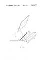
- FIG. 1a spool 10 of fiber optic cable which typically may be 0.003 inch diameter.
- Optic fiber 11is unreeled from spool 10 and fastened to one end of drum 13.
- drum 13rotates in a counter clockwise direction, as indicated by the arrow on the drum, optic fiber 11 forms a single layer winding 12a on drum 13.
- FIG. 1there is shown only a partial layer on drum 13, but when drum 13 is entirely covered with one winding layer two or three more single layer windings are wound on top of each other by going back and forth across drum 13.
- the final thicknessis in the order of 0.010 inches.
- the diameter and length of drum 13are chosen so that the required dimensions of the finished fiber optic bundle shown in FIG. 3, to be described hereinafter, are met.
- a flexible coatingis applied to the winding that holds each turn in the layer relationship.
- the coatingmay be applied only along a band parallel to the axis of drum 13, which approach is preferred.
- optic fiber 11 from spool 10may be severed.
- the next stepis to slit the single layer winding lengthwise along drum 13 parallel to the axis thereof. When only a band of flexible coating is applied, the cut must be through it so that the optic fiber ends are held in a fixed relationship.
- the fiber optic bundleis then removed from drum 13. All three fiber optic bundles may be manufactured in this manner.
- FIG. 2shows the flexible layer 12b of fiber optic fibers after being slit and removed from the drum 13. Only for simplicity of representation the multiple layer fiber optic bundle wound on drum 13 is not shown, but instead only a single layer as shown in FIGS. 1 through 5.
- the letters A-Fare used to identify particular corners and midpoints of the now flat layer of fiber optic fibers to help understand how the final shaped bundle of fiber optics is formed, as shown in FIG. 3, to implement the present invention.
- FIG. 3shows the final configuration of the one of the three fiber bundles used to provide linear scanning.
- corners A and Bare wrapped around a ring-shaped member, not shown, and fastened to the ring so that end of the fiber optic bundle now forms a circle as shown in FIG. 3.
- the length of the winding on drum 13equals the circumference of the circle formed by the bundle end A, E, B wrapped around the ring-shaped member.
- the diameter of drum 13equals the length AC of bundle 12b in FIG. 2.
- points A, E and Bare show for orientation purposes.
- the flat fiber optic bundle shown in FIG. 2also has an end, the corners of which are represented by the letters C, F, D.
- FIG. 2shows the ends, the corners of which are represented by the letters C, F, D.
- these ends of the fiber optic bundleare captured between two flat members, not shown, so that these ends of the fiber optic bundle from a straight line as represented in FIG. 3 by the letters C, F, D.
- the ends of the fiber optic bundle now formed as shown in FIG. 3 and represented by letters A, E, B and C, F, D,are trimmed and polished in a manner well known in the art. This finishes the fabrication of one end of the three fiber optic bundles, shown in FIG. 3, used to implement the invention as shown in detail in FIG. 4 which is now described.
- the other two fiber optic bundles required to implement the inventionstart as shown in FIG. 2 and one end of each is formed in the same circular manner as is bundle 12c. The other end of the remaining two bundles are not held flat but are bunched together. The assembly of all three fiber optic bundles is shown in FIG. 4.
- FIG. 4The assembled three bundles shown in FIG. 4 are not shown in FIG. 5 in order not to obscure other elements in FIG. 5.
- a view, G, G'parallel to the plane of the ends of the fiber optic fibers forming the ring represented by the letters A, E, B.
- FIG. 5is shown the same view, G, G', as a circle showing only the very ends of the fiber optic fibers formed in the circle A, E, B.
- the remainder of the assembled fiber optic bundles shown in FIG. 4are not shown so as not to obscure this figure.
- Laser 14is used to create a collimated beam of light having an approximate diameter of 0.003 to 0.005 inches, which beam is passed through electro-acoustic modulator 15 which is used to intensity modulate the beam for the purposes described further in this specification, such as carrying information.
- electro-acoustic modulator 15which is used to intensity modulate the beam for the purposes described further in this specification, such as carrying information.
- a laser diodemay be used.
- the intensity modulated laser beam 16travels a path which is perpendicular to and passes through the center of the circle formed by the ends of the fiber optic bundle represented by A, E, B.
- the deflect the laser light beam 16 piezoelectric deflection circuit 17, piezoelectric drive fiber 18 and a small mirror 19are utilized.
- Fiber 18is a fused silica fiber to the end of which is bonded mirror 19 utilizing an epoxy cement.
- a deflection signal generated by deflection drive circuit 20is applied to piezoelectric deflection circuit 17, fiber 18 is caused to move in a fashion to reflect modulated laser beam 16 that is impinging upon mirror 19 in a conical fashion as represented by ray 25 tracing circle 26.
- the reflected modulated light beam 25impinges upon the fiber ends 24 of fiber optic bundle 12c (not shown in further detail in FIG. 5). Reflected light beam 25 scans around the circle formed by the ends 24 of the fiber optic bundle with a constant velocity.
- the modulated light beam 25 impinging upon ends 24 of the fiber optic strands making up fiber optic bundle 12care converted to a very linear scan as is obvious by the formation of bundle 12c.
- the modulated light beamis scanned around the circle formed by the ends 24 of the fiber optic fibers from A to E to B to complete one circular scan, the light beams travel through the fibers of bundle 12c in an extremely linear fashion from C to F to D in the same period of time. In this manner a very linear scan is produced.
- the end C, F, D of fiber optic bundle 12cshown in both FIGS. 3 and 4, are located immediately adjacent to a xerographic drum to implement the xerographic process.
- modulated light exiting end C, D, F of fiber optic bundleis not applied to a xerographic drum, but rather is applied via a lens and a polygonal mirror to a large screen deflection system, as is shown in FIG. 6 and described in detail further in this specification.
- Iprovide two additional fiber optic bundles 23a and 23b which are fabricated in the same manner as bundle 12c but are only one or two fiber layers deep.
- Bundles 23a and 23bmay be separately wound from bundle 12c or may be concurrently wound.
- bundle or blanket 23bmay first be wound on drum 13 in FIG. 1. With or without cutting fuber strand 11, the winding process is stopped and the one or two layer thick bundle is coated with the flexible coating to hold blanket or bundle 23b together.
- a layer of paper, plastic or other materialmay or may not be wrapped around the winding for bundle 23b and the winding process is then restarted to wind blanket or bundle 12c on top of bundle 23b with or without the layer of paper, plastic or other material.
- the winding processis again stopped with or without cutting fiber 11.
- another paper, plastic or other materialmay or may not be placed over the winding for bundle 12c. Again the winding process is restarted and bundle or blanket 23a is wound over the top of bundle 12c.
- a flexible coatingis also applied to bundle 23a to hold the fibers in positional relationship in the bundle.
- the longitudinal cut or slit through the fibers of bundles 23b, 12c and 23ais made as previously described only for winding 12c and the three windings are removed from drum 13.
- one of the slit ends of all three bundlesare kept together and wrapped around and fastened to the ring-shaped member, previously described, and then the ends of the fibers in bundles 23b, 12c and 23a wrapped around the ring-shaped member are polished in a manner well known in the art.
- the final assembled form of bundles 12c, 23a and 23bare shown in FIG. 4.
- the other ends of bundles 23a, 23b and 12care separated.
- the ends C, F, D of bundle 12care captured between the flat members as previously described and polished.
- the ends of bundles 23a and 23bare each gathered together in a bunch and the ends are polished.
- fiber optic bundles 23a and 23balso are not shown in detail as in FIG. 4. Rather they are depicted as shown in FIG. 5 for ease of representation.
- the ends formed in a circle along with ends A, E, B of bundle 12care only shown as ends, with the remainder of bundles 23a and 23b being representatively shown by a few optic fibers having ends 27 and 28 respectively.
- Light exiting any of the bunched ends of bundles 23a and 23bis input to photocells 22a and 22b respectively for the feedback.
- Lenses or other means known in the artmay also be implemented as necessary to focus light output from optic fiber bundles 23a and 23b onto photocells 22a and 22b respectively.
- Photocell 22adetects any light in any one of the individual fibers of fiber optic bundle 23a.
- photocell 22bdetects light in any one of the fibers of bundle 23b.
- the outputs of photocells 22a and 22bare applied to feedback circuit 21 which generates a feedback signal that is applied to deflection drive circuit 20 to modify the conical scan represented by light ray 25.
- Deflection drive circuit 20responds thereto to increase the drive signal applied to piezoelectric deflection circuit 17 to deflect optic fiber 18 a greater amount so that beam 25 impinges only upon ends 24 of fiber optic bundle 12c.
- an out of round tracethat is a trace that impinges on end 24 for only part of a circle, is detected and a correction signal is generated by feedback circuit 21 that causes deflection circuit 17 to drive fiber 18 and mirror 19 so that reflected beam 25 impinges only on ends 24 of bundle 12c.
- the operation of the circuit just describedprovides for an ultra-linear light scan, does not utilize motor drives, polygonal mirrors or other complex, expensive electromechanical hardware, and is self adjusting.
- FIG. 6is shown an alternative embodiment of the invention.
- the modulated lightis manipulated in the manner now described to produce full field scanning on a surface.
- linear scanningis produced with modulated light exiting fibers of bundle 12c starting at corner D and progressing uniformly across bundle 12c to corner C.
- Modulated light exiting ends D, F, C of bundle 12cis first focused to a point as it passes through lens 29 and the point is at one of the surfaces of polygonal mirror 30. Following optic laws, the focused light beam is reflected from mirror 30 with the angle of incidence equalling the angle of reflection.
- the reflectioncauses the modulated light beam to fall upon flat surface 31.
- the light beam exiting the optical fiber at corner D of bundle 12chits point G on surface 31.
- the focused light beam reflected from polygonal mirror 30scans across surface 31 from point G to point H.
- polygonal mirror 30is incrementally rotated a small amount (by apparatus not shown) which changes the angle of incidence of the light beam on mirror 30. After each scan polygonal mirror 30 is rotated a small amount. In this manner the entire surface is scanned. With polygonal mirror 30 rotated counter clockwise, as shown by the arrow in FIG. 5, the light beam will scan from top to bottom of surface 31.
- Those skilled in the artmay add other mirrors and lenses to the simple flat surface scanner in FIG. 6 or may design many other optical systems requiring linear light scanning apparatus such as provided by my invention.
Landscapes
- Physics & Mathematics (AREA)
- Engineering & Computer Science (AREA)
- Multimedia (AREA)
- Signal Processing (AREA)
- General Physics & Mathematics (AREA)
- Optics & Photonics (AREA)
- Facsimile Scanning Arrangements (AREA)
Abstract
Description
Claims (6)
Priority Applications (1)
| Application Number | Priority Date | Filing Date | Title |
|---|---|---|---|
| US06/276,279US4409477A (en) | 1981-06-22 | 1981-06-22 | Scanning optical system |
Applications Claiming Priority (1)
| Application Number | Priority Date | Filing Date | Title |
|---|---|---|---|
| US06/276,279US4409477A (en) | 1981-06-22 | 1981-06-22 | Scanning optical system |
Publications (1)
| Publication Number | Publication Date |
|---|---|
| US4409477Atrue US4409477A (en) | 1983-10-11 |
Family
ID=23055995
Family Applications (1)
| Application Number | Title | Priority Date | Filing Date |
|---|---|---|---|
| US06/276,279Expired - Fee RelatedUS4409477A (en) | 1981-06-22 | 1981-06-22 | Scanning optical system |
Country Status (1)
| Country | Link |
|---|---|
| US (1) | US4409477A (en) |
Cited By (51)
| Publication number | Priority date | Publication date | Assignee | Title |
|---|---|---|---|---|
| US4491719A (en)* | 1982-12-20 | 1985-01-01 | General Electric Company | Light pattern projector especially for welding |
| US4516832A (en)* | 1982-06-23 | 1985-05-14 | International Business Machines Corporation | Apparatus for transformation of a collimated beam into a source of _required shape and numerical aperture |
| US4525630A (en)* | 1981-08-11 | 1985-06-25 | De La Rue Systems Limited | Apparatus for detecting tape on sheets |
| US4547666A (en)* | 1983-01-19 | 1985-10-15 | National Computer Systems, Inc. | Mark array sense reader with sequential output signals |
| US4560235A (en)* | 1982-09-22 | 1985-12-24 | Honeywell Inc. | Fiber optic condenser for an optical imaging system |
| US4614868A (en)* | 1984-10-12 | 1986-09-30 | Caterpillar Industrial Inc. | Fiber optic seam tracking apparatus |
| US4634879A (en)* | 1985-03-21 | 1987-01-06 | General Electric Company | Method and system for determining surface profile information |
| US4721851A (en)* | 1985-04-30 | 1988-01-26 | Ricoh Company, Ltd. | Image reading device using fiber optic bundles configured differently at each end |
| US4812012A (en)* | 1986-12-12 | 1989-03-14 | Mitsubishi Rayon Company Ltd. | Optical fiber array having fiber islands in a polymer sea |
| US4821114A (en)* | 1986-05-02 | 1989-04-11 | Dr. Ing. Rudolf Hell Gmbh | Opto-electronic scanning arrangement |
| WO1989008020A1 (en)* | 1988-03-03 | 1989-09-08 | Eastman Kodak Company | Light collector for stimulable phosphor imaging apparatus |
| US4866288A (en)* | 1985-09-24 | 1989-09-12 | Erwin Sick Gmbh Optik-Elektronik | Apparatus for optically scanning a web of material |
| US4899040A (en)* | 1988-09-08 | 1990-02-06 | Eastman Kodak Company | Light-conditioning apparatus for an image scanner illumination system |
| US4930849A (en)* | 1988-10-27 | 1990-06-05 | Pioneer Electronic Corporation | Laser scanning apparatus and method of scanning using same |
| US4974927A (en)* | 1987-06-18 | 1990-12-04 | Fuji Photo Film Co., Ltd. | Original-illuminating device for use in an image-reading device |
| US4991918A (en)* | 1988-03-03 | 1991-02-12 | Eastman Kodak Company | Light collector for stimulable phosphor imaging apparatus |
| US5015064A (en)* | 1990-04-05 | 1991-05-14 | Photon Imaging Corp. | Electronic printer or scanner using a fiber optic bundle |
| EP0435006A3 (en)* | 1989-12-23 | 1992-03-04 | Dornier Luftfahrt Gmbh | Fibre optic scanner |
| US5136678A (en)* | 1990-02-19 | 1992-08-04 | Brother Kogyo Kabushiki Kaisha | Optical wave guide array |
| US5328072A (en)* | 1987-10-17 | 1994-07-12 | J.M. Voith Gmbh | Device for locating the edges of moving webs |
| US5650868A (en)* | 1995-06-07 | 1997-07-22 | Compaq Computer Corporation | Data transfer system |
| US5701181A (en)* | 1995-05-12 | 1997-12-23 | Bayer Corporation | Fiber optic diffuse light reflectance sensor utilized in the detection of occult blood |
| US5828483A (en)* | 1993-11-23 | 1998-10-27 | Schwartz; Nira | Printing and inspection system using rotating polygon and optical fibers |
| WO2003046656A1 (en)* | 2001-11-21 | 2003-06-05 | Essex Electro Engineers, Inc. | Method and apparatus for radiographic imaging |
| US20030132395A1 (en)* | 2000-06-29 | 2003-07-17 | Essex Electro Engineers, Inc. | Method and apparatus for radiographic imaging |
| US20040021101A1 (en)* | 2000-06-29 | 2004-02-05 | Essex Electro Engineers, Inc. | Method and apparatus for radiographic imaging |
| US20070153350A1 (en)* | 2005-12-29 | 2007-07-05 | Samsung Electro-Mechanics Co., Ltd. | Laser projection display |
| US20080073163A1 (en)* | 2006-09-22 | 2008-03-27 | Weir Michael P | Micro-electromechanical device |
| US20080226034A1 (en)* | 2007-03-12 | 2008-09-18 | Weir Michael P | Power modulation of a scanning beam for imaging, therapy, and/or diagnosis |
| US20080242967A1 (en)* | 2007-03-27 | 2008-10-02 | Ethicon Endo-Surgery, Inc. | Medical imaging and therapy utilizing a scanned beam system operating at multiple wavelengths |
| US20080255458A1 (en)* | 2007-04-13 | 2008-10-16 | Ethicon Endo-Surgery, Inc. | System and method using fluorescence to examine within a patient's anatomy |
| US20080275305A1 (en)* | 2007-05-01 | 2008-11-06 | Ethicon Endo-Surgery, Inc. | Medical scanned beam imager and components associated therewith |
| US20080312490A1 (en)* | 2007-06-18 | 2008-12-18 | Ethicon Endo-Surgery, Inc. | Methods and devices for repairing damaged or diseased tissue using a scanning beam assembly |
| US20090062658A1 (en)* | 2007-08-27 | 2009-03-05 | Dunki-Jacobs Robert J | Position tracking and control for a scanning assembly |
| US20090060381A1 (en)* | 2007-08-31 | 2009-03-05 | Ethicon Endo-Surgery, Inc. | Dynamic range and amplitude control for imaging |
| US20090062659A1 (en)* | 2007-08-28 | 2009-03-05 | Weir Michael P | Medical device including scanned beam unit with operational control features |
| US7558455B2 (en)* | 2007-06-29 | 2009-07-07 | Ethicon Endo-Surgery, Inc | Receiver aperture broadening for scanned beam imaging |
| US7561317B2 (en) | 2006-11-03 | 2009-07-14 | Ethicon Endo-Surgery, Inc. | Resonant Fourier scanning |
| US7589316B2 (en) | 2007-01-18 | 2009-09-15 | Ethicon Endo-Surgery, Inc. | Scanning beam imaging with adjustable detector sensitivity or gain |
| US7713265B2 (en) | 2006-12-22 | 2010-05-11 | Ethicon Endo-Surgery, Inc. | Apparatus and method for medically treating a tattoo |
| US20100183272A1 (en)* | 2009-01-19 | 2010-07-22 | Eisuke Sasaoka | Optical fiber |
| US20100195965A1 (en)* | 2009-01-20 | 2010-08-05 | Eisuke Sasaoka | Optical communication system and arrangement converter |
| US20110052129A1 (en)* | 2009-01-19 | 2011-03-03 | Eisuke Sasaoka | Multi-core optical fiber |
| US7982776B2 (en) | 2007-07-13 | 2011-07-19 | Ethicon Endo-Surgery, Inc. | SBI motion artifact removal apparatus and method |
| US7995045B2 (en) | 2007-04-13 | 2011-08-09 | Ethicon Endo-Surgery, Inc. | Combined SBI and conventional image processor |
| US8050520B2 (en) | 2008-03-27 | 2011-11-01 | Ethicon Endo-Surgery, Inc. | Method for creating a pixel image from sampled data of a scanned beam imager |
| US8273015B2 (en) | 2007-01-09 | 2012-09-25 | Ethicon Endo-Surgery, Inc. | Methods for imaging the anatomy with an anatomically secured scanner assembly |
| US8332014B2 (en) | 2008-04-25 | 2012-12-11 | Ethicon Endo-Surgery, Inc. | Scanned beam device and method using same which measures the reflectance of patient tissue |
| EP2279375A4 (en)* | 2008-04-30 | 2014-04-16 | Carestream Health Inc | Variable condenser for delivery of illumination |
| US8801606B2 (en) | 2007-01-09 | 2014-08-12 | Ethicon Endo-Surgery, Inc. | Method of in vivo monitoring using an imaging system including scanned beam imaging unit |
| US9125552B2 (en) | 2007-07-31 | 2015-09-08 | Ethicon Endo-Surgery, Inc. | Optical scanning module and means for attaching the module to medical instruments for introducing the module into the anatomy |
Citations (5)
| Publication number | Priority date | Publication date | Assignee | Title |
|---|---|---|---|---|
| US4203672A (en)* | 1976-11-18 | 1980-05-20 | E. I. Du Pont De Nemours And Company | Scanning beam displacement compensation control system |
| US4214157A (en)* | 1978-07-07 | 1980-07-22 | Pitney Bowes, Inc. | Apparatus and method for correcting imperfection in a polygon used for laser scanning |
| US4222630A (en)* | 1977-08-03 | 1980-09-16 | Institut Francias Du Petrole | Digitally controlled fiber optic recording device |
| US4256959A (en)* | 1979-09-12 | 1981-03-17 | The Mead Corporation | Optical scanner including feedback for reflector control |
| US4352550A (en)* | 1979-12-13 | 1982-10-05 | Iwatsu Electric Co., Ltd. | Combination of circular/straight line light beam scan transforming apparatus and optical device and method of fabricating circular/straight line transforming device |
- 1981
- 1981-06-22USUS06/276,279patent/US4409477A/ennot_activeExpired - Fee Related
Patent Citations (5)
| Publication number | Priority date | Publication date | Assignee | Title |
|---|---|---|---|---|
| US4203672A (en)* | 1976-11-18 | 1980-05-20 | E. I. Du Pont De Nemours And Company | Scanning beam displacement compensation control system |
| US4222630A (en)* | 1977-08-03 | 1980-09-16 | Institut Francias Du Petrole | Digitally controlled fiber optic recording device |
| US4214157A (en)* | 1978-07-07 | 1980-07-22 | Pitney Bowes, Inc. | Apparatus and method for correcting imperfection in a polygon used for laser scanning |
| US4256959A (en)* | 1979-09-12 | 1981-03-17 | The Mead Corporation | Optical scanner including feedback for reflector control |
| US4352550A (en)* | 1979-12-13 | 1982-10-05 | Iwatsu Electric Co., Ltd. | Combination of circular/straight line light beam scan transforming apparatus and optical device and method of fabricating circular/straight line transforming device |
Cited By (66)
| Publication number | Priority date | Publication date | Assignee | Title |
|---|---|---|---|---|
| US4525630A (en)* | 1981-08-11 | 1985-06-25 | De La Rue Systems Limited | Apparatus for detecting tape on sheets |
| US4516832A (en)* | 1982-06-23 | 1985-05-14 | International Business Machines Corporation | Apparatus for transformation of a collimated beam into a source of _required shape and numerical aperture |
| US4560235A (en)* | 1982-09-22 | 1985-12-24 | Honeywell Inc. | Fiber optic condenser for an optical imaging system |
| US4491719A (en)* | 1982-12-20 | 1985-01-01 | General Electric Company | Light pattern projector especially for welding |
| US4547666A (en)* | 1983-01-19 | 1985-10-15 | National Computer Systems, Inc. | Mark array sense reader with sequential output signals |
| US4614868A (en)* | 1984-10-12 | 1986-09-30 | Caterpillar Industrial Inc. | Fiber optic seam tracking apparatus |
| US4634879A (en)* | 1985-03-21 | 1987-01-06 | General Electric Company | Method and system for determining surface profile information |
| US4721851A (en)* | 1985-04-30 | 1988-01-26 | Ricoh Company, Ltd. | Image reading device using fiber optic bundles configured differently at each end |
| US4866288A (en)* | 1985-09-24 | 1989-09-12 | Erwin Sick Gmbh Optik-Elektronik | Apparatus for optically scanning a web of material |
| US4821114A (en)* | 1986-05-02 | 1989-04-11 | Dr. Ing. Rudolf Hell Gmbh | Opto-electronic scanning arrangement |
| US4812012A (en)* | 1986-12-12 | 1989-03-14 | Mitsubishi Rayon Company Ltd. | Optical fiber array having fiber islands in a polymer sea |
| US4974927A (en)* | 1987-06-18 | 1990-12-04 | Fuji Photo Film Co., Ltd. | Original-illuminating device for use in an image-reading device |
| US5328072A (en)* | 1987-10-17 | 1994-07-12 | J.M. Voith Gmbh | Device for locating the edges of moving webs |
| WO1989008020A1 (en)* | 1988-03-03 | 1989-09-08 | Eastman Kodak Company | Light collector for stimulable phosphor imaging apparatus |
| US4991918A (en)* | 1988-03-03 | 1991-02-12 | Eastman Kodak Company | Light collector for stimulable phosphor imaging apparatus |
| US4899040A (en)* | 1988-09-08 | 1990-02-06 | Eastman Kodak Company | Light-conditioning apparatus for an image scanner illumination system |
| US4930849A (en)* | 1988-10-27 | 1990-06-05 | Pioneer Electronic Corporation | Laser scanning apparatus and method of scanning using same |
| EP0435006A3 (en)* | 1989-12-23 | 1992-03-04 | Dornier Luftfahrt Gmbh | Fibre optic scanner |
| US5136678A (en)* | 1990-02-19 | 1992-08-04 | Brother Kogyo Kabushiki Kaisha | Optical wave guide array |
| US5015064A (en)* | 1990-04-05 | 1991-05-14 | Photon Imaging Corp. | Electronic printer or scanner using a fiber optic bundle |
| US5828483A (en)* | 1993-11-23 | 1998-10-27 | Schwartz; Nira | Printing and inspection system using rotating polygon and optical fibers |
| US5701181A (en)* | 1995-05-12 | 1997-12-23 | Bayer Corporation | Fiber optic diffuse light reflectance sensor utilized in the detection of occult blood |
| US5650868A (en)* | 1995-06-07 | 1997-07-22 | Compaq Computer Corporation | Data transfer system |
| US6894303B2 (en)* | 2000-06-29 | 2005-05-17 | Essex Electro Engineers, Inc. | Method and apparatus for radiographic imaging |
| US20030132395A1 (en)* | 2000-06-29 | 2003-07-17 | Essex Electro Engineers, Inc. | Method and apparatus for radiographic imaging |
| US20040021101A1 (en)* | 2000-06-29 | 2004-02-05 | Essex Electro Engineers, Inc. | Method and apparatus for radiographic imaging |
| US6696698B2 (en)* | 2000-06-29 | 2004-02-24 | Essex Electro Engineers, Inc. | Method and apparatus for radiographic imaging |
| WO2003046656A1 (en)* | 2001-11-21 | 2003-06-05 | Essex Electro Engineers, Inc. | Method and apparatus for radiographic imaging |
| WO2004040947A3 (en)* | 2002-10-28 | 2005-03-10 | Essex Electro Engineers Inc | Method and apparatus for radiographic imaging |
| WO2004048897A3 (en)* | 2002-11-22 | 2005-05-06 | Essex Electro Engineers Inc | Method and apparatus for radiographic imaging |
| US20070153350A1 (en)* | 2005-12-29 | 2007-07-05 | Samsung Electro-Mechanics Co., Ltd. | Laser projection display |
| US7562986B2 (en)* | 2005-12-29 | 2009-07-21 | Samsung Electro-Mechanics Co., Ltd. | Laser projection display |
| US20080073163A1 (en)* | 2006-09-22 | 2008-03-27 | Weir Michael P | Micro-electromechanical device |
| US9079762B2 (en) | 2006-09-22 | 2015-07-14 | Ethicon Endo-Surgery, Inc. | Micro-electromechanical device |
| US7561317B2 (en) | 2006-11-03 | 2009-07-14 | Ethicon Endo-Surgery, Inc. | Resonant Fourier scanning |
| US7713265B2 (en) | 2006-12-22 | 2010-05-11 | Ethicon Endo-Surgery, Inc. | Apparatus and method for medically treating a tattoo |
| US8801606B2 (en) | 2007-01-09 | 2014-08-12 | Ethicon Endo-Surgery, Inc. | Method of in vivo monitoring using an imaging system including scanned beam imaging unit |
| US8273015B2 (en) | 2007-01-09 | 2012-09-25 | Ethicon Endo-Surgery, Inc. | Methods for imaging the anatomy with an anatomically secured scanner assembly |
| US7589316B2 (en) | 2007-01-18 | 2009-09-15 | Ethicon Endo-Surgery, Inc. | Scanning beam imaging with adjustable detector sensitivity or gain |
| US20080226034A1 (en)* | 2007-03-12 | 2008-09-18 | Weir Michael P | Power modulation of a scanning beam for imaging, therapy, and/or diagnosis |
| US8216214B2 (en) | 2007-03-12 | 2012-07-10 | Ethicon Endo-Surgery, Inc. | Power modulation of a scanning beam for imaging, therapy, and/or diagnosis |
| US20080242967A1 (en)* | 2007-03-27 | 2008-10-02 | Ethicon Endo-Surgery, Inc. | Medical imaging and therapy utilizing a scanned beam system operating at multiple wavelengths |
| US7995045B2 (en) | 2007-04-13 | 2011-08-09 | Ethicon Endo-Surgery, Inc. | Combined SBI and conventional image processor |
| US20080255458A1 (en)* | 2007-04-13 | 2008-10-16 | Ethicon Endo-Surgery, Inc. | System and method using fluorescence to examine within a patient's anatomy |
| US8626271B2 (en) | 2007-04-13 | 2014-01-07 | Ethicon Endo-Surgery, Inc. | System and method using fluorescence to examine within a patient's anatomy |
| US20080275305A1 (en)* | 2007-05-01 | 2008-11-06 | Ethicon Endo-Surgery, Inc. | Medical scanned beam imager and components associated therewith |
| US8160678B2 (en) | 2007-06-18 | 2012-04-17 | Ethicon Endo-Surgery, Inc. | Methods and devices for repairing damaged or diseased tissue using a scanning beam assembly |
| US20080312490A1 (en)* | 2007-06-18 | 2008-12-18 | Ethicon Endo-Surgery, Inc. | Methods and devices for repairing damaged or diseased tissue using a scanning beam assembly |
| US7558455B2 (en)* | 2007-06-29 | 2009-07-07 | Ethicon Endo-Surgery, Inc | Receiver aperture broadening for scanned beam imaging |
| US7982776B2 (en) | 2007-07-13 | 2011-07-19 | Ethicon Endo-Surgery, Inc. | SBI motion artifact removal apparatus and method |
| US9125552B2 (en) | 2007-07-31 | 2015-09-08 | Ethicon Endo-Surgery, Inc. | Optical scanning module and means for attaching the module to medical instruments for introducing the module into the anatomy |
| US20090062658A1 (en)* | 2007-08-27 | 2009-03-05 | Dunki-Jacobs Robert J | Position tracking and control for a scanning assembly |
| US7983739B2 (en) | 2007-08-27 | 2011-07-19 | Ethicon Endo-Surgery, Inc. | Position tracking and control for a scanning assembly |
| US7925333B2 (en) | 2007-08-28 | 2011-04-12 | Ethicon Endo-Surgery, Inc. | Medical device including scanned beam unit with operational control features |
| US20090062659A1 (en)* | 2007-08-28 | 2009-03-05 | Weir Michael P | Medical device including scanned beam unit with operational control features |
| US20090060381A1 (en)* | 2007-08-31 | 2009-03-05 | Ethicon Endo-Surgery, Inc. | Dynamic range and amplitude control for imaging |
| US8050520B2 (en) | 2008-03-27 | 2011-11-01 | Ethicon Endo-Surgery, Inc. | Method for creating a pixel image from sampled data of a scanned beam imager |
| US8332014B2 (en) | 2008-04-25 | 2012-12-11 | Ethicon Endo-Surgery, Inc. | Scanned beam device and method using same which measures the reflectance of patient tissue |
| EP2279375A4 (en)* | 2008-04-30 | 2014-04-16 | Carestream Health Inc | Variable condenser for delivery of illumination |
| US8447156B2 (en) | 2009-01-19 | 2013-05-21 | Sumitomo Electric Industries, Ltd. | Multi-core optical fiber |
| US8655131B2 (en) | 2009-01-19 | 2014-02-18 | Sumitomo Electric Industries, Ltd. | Multi-core optical fiber |
| US8687931B2 (en) | 2009-01-19 | 2014-04-01 | Sumitomo Electric Industries, Ltd. | Optical fiber |
| US20110052129A1 (en)* | 2009-01-19 | 2011-03-03 | Eisuke Sasaoka | Multi-core optical fiber |
| US20100183272A1 (en)* | 2009-01-19 | 2010-07-22 | Eisuke Sasaoka | Optical fiber |
| US8320724B2 (en)* | 2009-01-20 | 2012-11-27 | Sumitomo Electric Industries, Ltd. | Optical communication system and arrangement converter |
| US20100195965A1 (en)* | 2009-01-20 | 2010-08-05 | Eisuke Sasaoka | Optical communication system and arrangement converter |
Similar Documents
| Publication | Publication Date | Title |
|---|---|---|
| US4409477A (en) | Scanning optical system | |
| US4904034A (en) | Scanning apparatus | |
| JPH0617948B2 (en) | Optical beam scanning device | |
| EP0288970A2 (en) | Optical system for flyingspot scanning system | |
| US5475523A (en) | Disk for light beam recording device and light beam recording device | |
| JPS63241519A (en) | Light beam recorder | |
| US6118471A (en) | Beam diameter control method and device | |
| US4281889A (en) | Light beam scanning system | |
| JPS6115119A (en) | Laser printer | |
| EP0186920B1 (en) | Focus-corrected convergent beam scanner | |
| JP3460440B2 (en) | Multi-beam scanning optical device | |
| JP2992075B2 (en) | Light beam scanning device | |
| JPH10123448A (en) | Scanning optical device | |
| JPS60107016A (en) | Device for obtaining parallel scanning luminous flux from incident luminous flux | |
| JPH01239520A (en) | Beam deflecting device and beam scanning device | |
| JPS6125118A (en) | laser printer | |
| JPH03200114A (en) | Exposure correcting device for laser scanning optical system using light transparent mirror | |
| JPS6159411A (en) | Laser printer | |
| JPS59202431A (en) | Laser beam scanner | |
| JPH0625830B2 (en) | Optical scanning device | |
| JPS60194418A (en) | Laser beam scanning system | |
| JPS61153615A (en) | Rotating polygon mirror rotation speed detection device | |
| JPH0131167B2 (en) | ||
| JPH03209417A (en) | optical scanning device | |
| JPH04110816A (en) | optical scanning device |
Legal Events
| Date | Code | Title | Description |
|---|---|---|---|
| AS | Assignment | Owner name:SANDERS ASSOCIATES, DANIEL WEBSTER HIGHWAY SOUTH, Free format text:ASSIGNMENT OF ASSIGNORS INTEREST.;ASSIGNOR:CARL, NORMAN J.;REEL/FRAME:003926/0796 Effective date:19810616 | |
| PA | Patent available for licence or sale | ||
| MAFP | Maintenance fee payment | Free format text:PAYMENT OF MAINTENANCE FEE, 4TH YEAR, PL 96-517 (ORIGINAL EVENT CODE: M170); ENTITY STATUS OF PATENT OWNER: LARGE ENTITY Year of fee payment:4 | |
| AS | Assignment | Owner name:CALCOMP INC., 2411 WEST LA PALMA AVENUE, ANAHEIM, Free format text:ASSIGNMENT OF ASSIGNORS INTEREST.;ASSIGNOR:SANDERS ASSOCIATES, INC.;REEL/FRAME:004914/0460 Effective date:19880630 | |
| MAFP | Maintenance fee payment | Free format text:PAYMENT OF MAINTENANCE FEE, 8TH YEAR, PL 96-517 (ORIGINAL EVENT CODE: M171); ENTITY STATUS OF PATENT OWNER: LARGE ENTITY Year of fee payment:8 | |
| FEPP | Fee payment procedure | Free format text:PAYOR NUMBER ASSIGNED (ORIGINAL EVENT CODE: ASPN); ENTITY STATUS OF PATENT OWNER: LARGE ENTITY | |
| FEPP | Fee payment procedure | Free format text:MAINTENANCE FEE REMINDER MAILED (ORIGINAL EVENT CODE: REM.); ENTITY STATUS OF PATENT OWNER: LARGE ENTITY | |
| LAPS | Lapse for failure to pay maintenance fees | ||
| FP | Lapsed due to failure to pay maintenance fee | Effective date:19951011 | |
| STCH | Information on status: patent discontinuation | Free format text:PATENT EXPIRED DUE TO NONPAYMENT OF MAINTENANCE FEES UNDER 37 CFR 1.362 |