US4407934A - Method of making an assembly of electrodes - Google Patents
Method of making an assembly of electrodesDownload PDFInfo
- Publication number
- US4407934A US4407934AUS06/327,598US32759881AUS4407934AUS 4407934 AUS4407934 AUS 4407934AUS 32759881 AUS32759881 AUS 32759881AUS 4407934 AUS4407934 AUS 4407934A
- Authority
- US
- United States
- Prior art keywords
- plate
- electrodes
- glass
- slots
- strip portions
- Prior art date
- Legal status (The legal status is an assumption and is not a legal conclusion. Google has not performed a legal analysis and makes no representation as to the accuracy of the status listed.)
- Expired - Lifetime
Links
- 238000004519manufacturing processMethods0.000titledescription4
- 239000011521glassSubstances0.000claimsabstractdescription36
- 238000000034methodMethods0.000claimsdescription23
- 230000005855radiationEffects0.000claimsdescription14
- KRHYYFGTRYWZRS-UHFFFAOYSA-NFluoraneChemical compoundFKRHYYFGTRYWZRS-UHFFFAOYSA-N0.000claimsdescription8
- 239000002253acidSubstances0.000claimsdescription6
- 229910052500inorganic mineralInorganic materials0.000claimsdescription5
- 239000011707mineralSubstances0.000claimsdescription5
- PXHVJJICTQNCMI-UHFFFAOYSA-NNickelChemical compound[Ni]PXHVJJICTQNCMI-UHFFFAOYSA-N0.000claimsdescription4
- 229910001515alkali metal fluorideInorganic materials0.000claimsdescription4
- PAZHGORSDKKUPI-UHFFFAOYSA-Nlithium metasilicateChemical compound[Li+].[Li+].[O-][Si]([O-])=OPAZHGORSDKKUPI-UHFFFAOYSA-N0.000claimsdescription4
- 229910052912lithium silicateInorganic materials0.000claimsdescription4
- 229910052751metalInorganic materials0.000claimsdescription4
- 239000002184metalSubstances0.000claimsdescription4
- 239000002904solventSubstances0.000claimsdescription4
- 238000000137annealingMethods0.000claimsdescription3
- 239000013078crystalSubstances0.000claimsdescription3
- 230000008020evaporationEffects0.000claimsdescription2
- 238000001704evaporationMethods0.000claimsdescription2
- 229910052759nickelInorganic materials0.000claimsdescription2
- 238000007747platingMethods0.000claimsdescription2
- 238000001552radio frequency sputter depositionMethods0.000claimsdescription2
- 238000012216screeningMethods0.000claimsdescription2
- 239000010935stainless steelSubstances0.000claimsdescription2
- 229910001220stainless steelInorganic materials0.000claimsdescription2
- 238000007740vapor depositionMethods0.000claimsdescription2
- 229910001092metal group alloyInorganic materials0.000claims1
- 239000000463materialSubstances0.000abstractdescription7
- 239000006089photosensitive glassSubstances0.000abstractdescription5
- 239000002241glass-ceramicSubstances0.000description9
- 229910011763Li2 OInorganic materials0.000description4
- VYPSYNLAJGMNEJ-UHFFFAOYSA-NSilicium dioxideChemical compoundO=[Si]=OVYPSYNLAJGMNEJ-UHFFFAOYSA-N0.000description4
- 238000000429assemblyMethods0.000description4
- 230000000712assemblyEffects0.000description4
- 238000010438heat treatmentMethods0.000description4
- 239000011810insulating materialSubstances0.000description4
- 229910018404Al2 O3Inorganic materials0.000description3
- 238000002360preparation methodMethods0.000description3
- 229910004742Na2 OInorganic materials0.000description2
- 206010034972Photosensitivity reactionDiseases0.000description2
- 229910021607Silver chlorideInorganic materials0.000description2
- 150000007513acidsChemical class0.000description2
- 239000000919ceramicSubstances0.000description2
- 229910052681coesiteInorganic materials0.000description2
- 239000002131composite materialSubstances0.000description2
- 229910052906cristobaliteInorganic materials0.000description2
- 238000002425crystallisationMethods0.000description2
- 230000008025crystallizationEffects0.000description2
- 239000010931goldSubstances0.000description2
- 238000003754machiningMethods0.000description2
- 239000011159matrix materialSubstances0.000description2
- 230000004048modificationEffects0.000description2
- 238000012986modificationMethods0.000description2
- 239000011022opalSubstances0.000description2
- 230000036211photosensitivityEffects0.000description2
- 239000005394sealing glassSubstances0.000description2
- 239000000377silicon dioxideSubstances0.000description2
- 229910052709silverInorganic materials0.000description2
- HKZLPVFGJNLROG-UHFFFAOYSA-Msilver monochlorideChemical compound[Cl-].[Ag+]HKZLPVFGJNLROG-UHFFFAOYSA-M0.000description2
- 229910052682stishoviteInorganic materials0.000description2
- 239000000126substanceSubstances0.000description2
- 230000009466transformationEffects0.000description2
- 229910052905tridymiteInorganic materials0.000description2
- RYGMFSIKBFXOCR-UHFFFAOYSA-NCopperChemical compound[Cu]RYGMFSIKBFXOCR-UHFFFAOYSA-N0.000description1
- 239000006088FotoceramSubstances0.000description1
- WHXSMMKQMYFTQS-UHFFFAOYSA-NLithiumChemical compound[Li]WHXSMMKQMYFTQS-UHFFFAOYSA-N0.000description1
- 239000000956alloySubstances0.000description1
- 229910045601alloyInorganic materials0.000description1
- 238000003491arrayMethods0.000description1
- CETPSERCERDGAM-UHFFFAOYSA-Nceric oxideChemical compoundO=[Ce]=OCETPSERCERDGAM-UHFFFAOYSA-N0.000description1
- 229910000422cerium(IV) oxideInorganic materials0.000description1
- 229910052802copperInorganic materials0.000description1
- 239000010949copperSubstances0.000description1
- 238000005553drillingMethods0.000description1
- -1e.g.Substances0.000description1
- 230000000694effectsEffects0.000description1
- PCHJSUWPFVWCPO-UHFFFAOYSA-NgoldChemical compound[Au]PCHJSUWPFVWCPO-UHFFFAOYSA-N0.000description1
- 229910052737goldInorganic materials0.000description1
- 238000011065in-situ storageMethods0.000description1
- 229910052744lithiumInorganic materials0.000description1
- 238000003801millingMethods0.000description1
- 239000000203mixtureSubstances0.000description1
- 238000004080punchingMethods0.000description1
- 238000007789sealingMethods0.000description1
- 239000004332silverSubstances0.000description1
Images

Classifications
- H—ELECTRICITY
- H01—ELECTRIC ELEMENTS
- H01J—ELECTRIC DISCHARGE TUBES OR DISCHARGE LAMPS
- H01J17/00—Gas-filled discharge tubes with solid cathode
- H01J17/38—Cold-cathode tubes
- H01J17/48—Cold-cathode tubes with more than one cathode or anode, e.g. sequence-discharge tube, counting tube, dekatron
- H01J17/49—Display panels, e.g. with crossed electrodes, e.g. making use of direct current
- H01J17/492—Display panels, e.g. with crossed electrodes, e.g. making use of direct current with crossed electrodes
- H—ELECTRICITY
- H01—ELECTRIC ELEMENTS
- H01J—ELECTRIC DISCHARGE TUBES OR DISCHARGE LAMPS
- H01J9/00—Apparatus or processes specially adapted for the manufacture, installation, removal, maintenance of electric discharge tubes, discharge lamps, or parts thereof; Recovery of material from discharge tubes or lamps
- H01J9/02—Manufacture of electrodes or electrode systems
Definitions
- Glasses, glass-ceramics, and sintered ceramicsdemonstrate high refractoriness, good chemical resistance to the ambient environment, relative inertness to impinging radiations of various wavelengths, and high mechanical strength but are difficult to drill, punch, or otherwise mechanically shape into complex geometries.
- the opal glasses describedconsist essentially, expressed in weight percent on the oxide basis, of 9-15% Li 2 O, 0-8% total Na 2 O and/or K 2 O, 9-23% Li 2 O+Na 2 O+K 2 O, 70-85% SiO 2 , 0.001-0.020% Ag, computed as AgCl, 0-10% Al 2 O 3 , 0-2.4% F, and 0-0.05% CeO 2 .
- portions of such glass bodiesare exposed to short wave radiation, customarily ultraviolet radiation, a latent image is produced in those portions.
- the glass-ceramic articles disclosed in U.S. Pat. No. 2,971,853consist essentially, expressed in weight percent on the oxide basis, of 60-85% SiO 2 , 5.5-15% Li 2 O, 2-25% Al 2 O 3 , the ratio Al 2 O 3 :Li 2 O being less than 1.7:1, and a photosensitive metal in the indicated proportions selected from the group of 0.001-0.03% gold, computed as Au, 0.001-0.3% silver, computed as AgCl, and 0.001-1% copper, computed as CuO.
- a latent imageis produced in those portions.
- those previously-exposed areas of glass bodiesare subjected to a two-step heat treatment.
- those portionsare initially subjected to temperatures between the annealing and softening points of the glass, and then to temperatures above the softening point of the glass.
- This latter stepeffects crystallization in situ in the previously-exposed portions of the bodies, the unexposed portions being essentially unchanged.
- the exposed areasare highly crystalline and include at least one lithium-containing crystal phase which is more readily soluble in mineral acids, e.g., dilute hydrofluoric acid, than the residual glass.
- Chemically-sculpturable, photosensitive glasses and glass-ceramicshave been employed commercially in a number of applications including electronic and fluidic devices where grooves, slots, holes, etc., of high tolerances have been etched therein.
- Corning Glass Works, Corning, New Yorkhas marketed a chemically machinable, photosensitive glass product under the trademark FOTOFORM and chemically machinable glass-ceramic product under the trademark FOTOCERAM.
- the principal objective of the inventionis to provide an improved method for fabricating electrode assemblies comprising two sets of electrodes spaced apart in operative relation with each other in which the supporting structure therfor is of such complex geometry that removal of material from the supporting structure is conventionally demanded, said inventive method eliminating the need for machining, milling, drilling, punching, or other mechanical means for removing material from the supporting structure.
- Another objective of the inventionis to fabricate electrode assemblies which can be incorporated into gas-filled display panels or into other types of devices that utilize crossed electrodes and cell matrices.
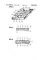
- FIG. 1is a plan view of a plate of electrical insulating material at one stage in the preparation of an assembly according to the inventive method
- FIG. 2is a sectional view through the plate of FIG. 1 along the lines 2--2 in FIG. 1;
- FIG. 3illustrates the composite article formed incorporating the plate of FIG. 2 at a later stage in the preparation of an assembly according to the inventive method
- FIG. 4is a perspective view of the completed assembly prepared from the composite article of FIG. 3;
- FIG. 5is a sectional view of a modification of the inventive assembly.
- FIG. 6is a sectional view of the assembly of FIG. 5 at a later stage in its preparation.
- the method of the inventioncomprises five general steps:
- a plate of photosensitive, electrical insulating materialis exposed to actinic radiation, commonly ultraviolet radiation, to develop a latent image therein in a selected pattern;
- said plateis heat-treated in a manner to develop a phase in the previously-exposed portions which can be selectively chemically remove from said plate material;
- an array of electrodese.g., anodes, is disposed onto one surface of said plate in alignment with said exposed and developed portions;
- an array of electrodese.g., cathodes is disposed onto the opposite surface of said plate oriented transversely to said first array of electrodes;
- said plate in at least said exposed and developed portionsis contacted with a solvent to selectively remove said phase in said exposed and developed portions, thereby producing slots in said plate and placing said arrays of electrodes in operative relation with each other.
- a plate 10 of a photosensitive glassis subjected to collimated ultraviolet radiation through a patterned mask composed of material opaque to ultraviolet radiation, or in some other manner, to produce latent images in the form of parallel, linear exposed regions 20 which pass through the body of plate 10 as is seen in FIG. 2. It can be observed in FIG. 1 that regions 20 do not extend to the edges of plate 10. This practice enables the edge portions of plate 10 to remain in place, thereby serving to maintain the integrity of plate 10 when portions thereof are subsequently removed from exposed regions 20. It will be recognized, of course, that other arrangements can be devised to hold plate 10 together after exposed regions 20 have been chemically removed. Plate 10 is then heated to a temperature generally below the softening point of the glass, but above the transformation range thereof, to develop crystallites in exposed regions 20 selected from the group of a lithium silicate and an alkali metal fluoride.
- an array of parallel, linear electrodes 30, to be operated as anode electrodesis formed by any suitable process, on the bottom surface 12 of plate 10. Electrodes 30 are aligned with exposed and developed regions 20. As illustrated in FIG. 2, anodes 30 are represented as flat, strip-like bodies which may be of any suitable width.
- FIG. 3an array of parallel, linear electrodes 40, to be operated as glow cathodes, is applied via any convenient technique to the top surface 14 of plate 10 oriented transversely to anode electrodes 30.
- FIGS. 3 and 4represent these cathodes as flat-strip-like bodies of any desired width.
- the crystallized portions 20are contacted with a mineral acid, e.g., dilute hydrofluoric acid, to dissolve those portions, thereby forming open slots 50 and leaving a structure as represented in FIG. 3.
- a mineral acide.g., dilute hydrofluoric acid
- FIG. 4an assembly is fabricated, as illustrated in FIG. 4, which comprises plate 10 having an array of slots 50 with an anode electrode 30 aligned with each slot and a plurality of cathode electrodes 40 disposed across slots 50.
- This assemblyafter the attachment of leads thereto, can be incorporated into a gas-filled display panel or other type of device.
- the anodes and cathodescan be formed from any suitable material which is highly electrically conducting and exhibits a coefficient of thermal expansion relatively closely matching that of the plate material.
- the electrodeswill be metallic, fabricated from stainless steel, nickel, or an alloy demonstrating the required expansion properties. Methods for applying the electrodes include, but are not limited to, evaporation, silk screening, RF sputtering, electroless metal and galvanic plating, and vapor deposition.
- FIGS. 5 and 6illustrate a modification of the basic method depicted in FIGS. 1-4.
- plate 10is subjected to collimated ultraviolet radiation through a patterned mask to produce latent images in the form of parallel, linear exposed regions 20 which pass through the body of plate 10. Thereafter, plate 10 is heat-treated at temperatures between the transformation range and the softening point of the glass to develop crystallites selected from the group of a lithium silicate and an alkali metal fluoride in regions 20.
- An array of parallel, linear cathode electrodes 40is applied via any suitable method to the top surface 14 of plate 10 in transverse orientation to crystallized regions 20.
- a plurality of parallel, linear anodes 30is applied through any convenient means to the surface of support plate 60.
- Support plate 60is prepared from an electrical insulating material, e.g., glass, and is oriented in such relation to plate 10 that anodes 30 are aligned with crystallized regions 20 of plate 10.
- plate 10is attached to support plate 60 via any suitable means.
- a sealing glass frit having a fusing temperature lower than those of plates 10 and 60is applied to contact areas on plate 10 and/or support plate 60.
- the assemblyis then fired at a sufficiently high temperature to fuse the sealing glass frit and thereby bond plates 10 and 60 together.
- crystallized portions 20are contacted with a mineral acid to etch out those regions leaving open slots 50.
- the completed assemblycomprises a matrix of cells which, after the attachment of leads thereto, can be utilized in a gas-filled display panel or other type of device which employs crossed electrodes and cell matrices. While not a requirement, the leads will desirably also be covered with a frit at the point of attachment to provide a measure of protection from mechanical abuse and atmospheric weathering.
- inventive assembliesreadily lend themselves to the production of multi-unit structures since two or more individual units can be laid up in a desired configuration and bonded together through conventional frit sealing or other means.
- the heat treatmentwill follow the manner disclosed in U.S. Pat. No. 2,971,853 and will consist of, first, subjecting the glass to temperatures between the annealing point and softening point thereof and, second, heating to temperatures above the softening point of the glass to develop a high degree of crystallization in the portions of the glass which were previously exposed to short wave radiation.
Landscapes
- Engineering & Computer Science (AREA)
- Manufacturing & Machinery (AREA)
- Glass Compositions (AREA)
- Gas-Filled Discharge Tubes (AREA)
- Surface Treatment Of Glass (AREA)
Abstract
Description
Claims (12)
Priority Applications (5)
| Application Number | Priority Date | Filing Date | Title |
|---|---|---|---|
| US06/327,598US4407934A (en) | 1981-12-04 | 1981-12-04 | Method of making an assembly of electrodes |
| JP83500315AJPS58502075A (en) | 1981-12-04 | 1982-12-01 | How to manufacture electrode assemblies |
| PCT/US1982/001696WO1983002034A1 (en) | 1981-12-04 | 1982-12-01 | Method of making an assembly of electrodes |
| EP82306456AEP0081359B1 (en) | 1981-12-04 | 1982-12-03 | Method of making an assembly of electrodes |
| DE8282306456TDE3270679D1 (en) | 1981-12-04 | 1982-12-03 | Method of making an assembly of electrodes |
Applications Claiming Priority (1)
| Application Number | Priority Date | Filing Date | Title |
|---|---|---|---|
| US06/327,598US4407934A (en) | 1981-12-04 | 1981-12-04 | Method of making an assembly of electrodes |
Publications (1)
| Publication Number | Publication Date |
|---|---|
| US4407934Atrue US4407934A (en) | 1983-10-04 |
Family
ID=23277217
Family Applications (1)
| Application Number | Title | Priority Date | Filing Date |
|---|---|---|---|
| US06/327,598Expired - LifetimeUS4407934A (en) | 1981-12-04 | 1981-12-04 | Method of making an assembly of electrodes |
Country Status (5)
| Country | Link |
|---|---|
| US (1) | US4407934A (en) |
| EP (1) | EP0081359B1 (en) |
| JP (1) | JPS58502075A (en) |
| DE (1) | DE3270679D1 (en) |
| WO (1) | WO1983002034A1 (en) |
Cited By (9)
| Publication number | Priority date | Publication date | Assignee | Title |
|---|---|---|---|---|
| US4532453A (en)* | 1982-12-03 | 1985-07-30 | Iwatsu Electric Co., Ltd. | Storage target for storage tubes and method of fabrication |
| US5083958A (en)* | 1990-07-16 | 1992-01-28 | Hughes Aircraft Company | Field emitter structure and fabrication process providing passageways for venting of outgassed materials from active electronic area |
| US5104343A (en)* | 1989-10-26 | 1992-04-14 | Matsushita Electric Industrial Co., Ltd. | Method for manufacturing flat display device |
| US5462467A (en)* | 1993-09-08 | 1995-10-31 | Silicon Video Corporation | Fabrication of filamentary field-emission device, including self-aligned gate |
| US5503582A (en)* | 1994-11-18 | 1996-04-02 | Micron Display Technology, Inc. | Method for forming spacers for display devices employing reduced pressures |
| US5562516A (en)* | 1993-09-08 | 1996-10-08 | Silicon Video Corporation | Field-emitter fabrication using charged-particle tracks |
| US5827099A (en)* | 1993-09-08 | 1998-10-27 | Candescent Technologies Corporation | Use of early formed lift-off layer in fabricating gated electron-emitting devices |
| US20030168580A1 (en)* | 2002-03-07 | 2003-09-11 | Cis Institut Fur Mikrosensorik Gmbh | Sensor detecting reflected light and method for its manufacture |
| US20070086874A1 (en)* | 2005-07-14 | 2007-04-19 | Paul Sullivan | Reactive Fasteners |
Families Citing this family (2)
| Publication number | Priority date | Publication date | Assignee | Title |
|---|---|---|---|---|
| JP2835430B2 (en)* | 1995-10-30 | 1998-12-14 | 株式会社住友金属エレクトロデバイス | Method of manufacturing plasma display panel barrier |
| AU2313700A (en)* | 1999-03-04 | 2000-09-21 | Electrovac, Fabrikation, elektrotechnischer Spezialartikel Gesellschaft m.b.H. | Cathode structure for a field emission display |
Citations (15)
| Publication number | Priority date | Publication date | Assignee | Title |
|---|---|---|---|---|
| US2628160A (en)* | 1951-08-30 | 1953-02-10 | Corning Glass Works | Sculpturing glass |
| US2684911A (en)* | 1951-08-30 | 1954-07-27 | Corning Glass Works | Photosensitively opacifiable glass |
| US2879147A (en)* | 1956-08-17 | 1959-03-24 | Houston R Baker | Method of etching glass |
| US2933648A (en)* | 1956-08-14 | 1960-04-19 | Gen Electric | Information display apparatus |
| US2971853A (en)* | 1953-03-05 | 1961-02-14 | Corning Glass Works | Ceramic body and method of making it |
| US3687513A (en)* | 1971-03-24 | 1972-08-29 | Burroughs Corp | Method of aging a display panel |
| US3704052A (en)* | 1971-05-03 | 1972-11-28 | Ncr Co | Method of making a plasma display panel |
| US3776613A (en)* | 1970-03-20 | 1973-12-04 | Philips Corp | Gas-discharge display panel |
| US3781984A (en)* | 1971-07-15 | 1974-01-01 | Fujitsu Ltd | Method for manufacturing electrodes of a display device utilizing gas discharge |
| US3787106A (en)* | 1971-11-09 | 1974-01-22 | Owens Illinois Inc | Monolithically structured gas discharge device and method of fabrication |
| US3789470A (en)* | 1968-06-12 | 1974-02-05 | Fujitsu Ltd | Method of manufacture of display device utilizing gas discharge |
| US3973815A (en)* | 1973-05-29 | 1976-08-10 | Owens-Illinois, Inc. | Assembly and sealing of gas discharge panel |
| US4092166A (en)* | 1976-12-27 | 1978-05-30 | International Business Machines Corporation | Double exposure and double etch technique for producing precision parts from crystallizable photosensitive glass |
| US4108521A (en)* | 1976-08-30 | 1978-08-22 | Burroughs Corporation | Method of making a display panel and the anodes therefor |
| US4276335A (en)* | 1978-03-13 | 1981-06-30 | General Electric Company | Electron beam matrix deflector and method of fabrication |
- 1981
- 1981-12-04USUS06/327,598patent/US4407934A/ennot_activeExpired - Lifetime
- 1982
- 1982-12-01JPJP83500315Apatent/JPS58502075A/enactiveGranted
- 1982-12-01WOPCT/US1982/001696patent/WO1983002034A1/enunknown
- 1982-12-03EPEP82306456Apatent/EP0081359B1/ennot_activeExpired
- 1982-12-03DEDE8282306456Tpatent/DE3270679D1/ennot_activeExpired
Patent Citations (15)
| Publication number | Priority date | Publication date | Assignee | Title |
|---|---|---|---|---|
| US2684911A (en)* | 1951-08-30 | 1954-07-27 | Corning Glass Works | Photosensitively opacifiable glass |
| US2628160A (en)* | 1951-08-30 | 1953-02-10 | Corning Glass Works | Sculpturing glass |
| US2971853A (en)* | 1953-03-05 | 1961-02-14 | Corning Glass Works | Ceramic body and method of making it |
| US2933648A (en)* | 1956-08-14 | 1960-04-19 | Gen Electric | Information display apparatus |
| US2879147A (en)* | 1956-08-17 | 1959-03-24 | Houston R Baker | Method of etching glass |
| US3789470A (en)* | 1968-06-12 | 1974-02-05 | Fujitsu Ltd | Method of manufacture of display device utilizing gas discharge |
| US3776613A (en)* | 1970-03-20 | 1973-12-04 | Philips Corp | Gas-discharge display panel |
| US3687513A (en)* | 1971-03-24 | 1972-08-29 | Burroughs Corp | Method of aging a display panel |
| US3704052A (en)* | 1971-05-03 | 1972-11-28 | Ncr Co | Method of making a plasma display panel |
| US3781984A (en)* | 1971-07-15 | 1974-01-01 | Fujitsu Ltd | Method for manufacturing electrodes of a display device utilizing gas discharge |
| US3787106A (en)* | 1971-11-09 | 1974-01-22 | Owens Illinois Inc | Monolithically structured gas discharge device and method of fabrication |
| US3973815A (en)* | 1973-05-29 | 1976-08-10 | Owens-Illinois, Inc. | Assembly and sealing of gas discharge panel |
| US4108521A (en)* | 1976-08-30 | 1978-08-22 | Burroughs Corporation | Method of making a display panel and the anodes therefor |
| US4092166A (en)* | 1976-12-27 | 1978-05-30 | International Business Machines Corporation | Double exposure and double etch technique for producing precision parts from crystallizable photosensitive glass |
| US4276335A (en)* | 1978-03-13 | 1981-06-30 | General Electric Company | Electron beam matrix deflector and method of fabrication |
Cited By (15)
| Publication number | Priority date | Publication date | Assignee | Title |
|---|---|---|---|---|
| US4532453A (en)* | 1982-12-03 | 1985-07-30 | Iwatsu Electric Co., Ltd. | Storage target for storage tubes and method of fabrication |
| US5104343A (en)* | 1989-10-26 | 1992-04-14 | Matsushita Electric Industrial Co., Ltd. | Method for manufacturing flat display device |
| US5083958A (en)* | 1990-07-16 | 1992-01-28 | Hughes Aircraft Company | Field emitter structure and fabrication process providing passageways for venting of outgassed materials from active electronic area |
| US5851669A (en)* | 1993-09-08 | 1998-12-22 | Candescent Technologies Corporation | Field-emission device that utilizes filamentary electron-emissive elements and typically has self-aligned gate |
| US5562516A (en)* | 1993-09-08 | 1996-10-08 | Silicon Video Corporation | Field-emitter fabrication using charged-particle tracks |
| US5813892A (en)* | 1993-09-08 | 1998-09-29 | Candescent Technologies Corporation | Use of charged-particle tracks in fabricating electron-emitting device having resistive layer |
| US5827099A (en)* | 1993-09-08 | 1998-10-27 | Candescent Technologies Corporation | Use of early formed lift-off layer in fabricating gated electron-emitting devices |
| US5462467A (en)* | 1993-09-08 | 1995-10-31 | Silicon Video Corporation | Fabrication of filamentary field-emission device, including self-aligned gate |
| US5913704A (en)* | 1993-09-08 | 1999-06-22 | Candescent Technologies Corporation | Fabrication of electronic devices by method that involves ion tracking |
| US6204596B1 (en)* | 1993-09-08 | 2001-03-20 | Candescent Technologies Corporation | Filamentary electron-emission device having self-aligned gate or/and lower conductive/resistive region |
| US5503582A (en)* | 1994-11-18 | 1996-04-02 | Micron Display Technology, Inc. | Method for forming spacers for display devices employing reduced pressures |
| US5698932A (en)* | 1994-11-18 | 1997-12-16 | Micron Display Technology, Inc. | Interelectrode spacers for display devices including field emission displays |
| US20030168580A1 (en)* | 2002-03-07 | 2003-09-11 | Cis Institut Fur Mikrosensorik Gmbh | Sensor detecting reflected light and method for its manufacture |
| US7030359B2 (en)* | 2002-03-07 | 2006-04-18 | CiS Institut für Mikrosensorik gGmbH | Sensor detecting reflected light and method for its manufacture |
| US20070086874A1 (en)* | 2005-07-14 | 2007-04-19 | Paul Sullivan | Reactive Fasteners |
Also Published As
| Publication number | Publication date |
|---|---|
| WO1983002034A1 (en) | 1983-06-09 |
| JPS58502075A (en) | 1983-12-01 |
| EP0081359B1 (en) | 1986-04-16 |
| EP0081359A1 (en) | 1983-06-15 |
| JPH0574175B2 (en) | 1993-10-15 |
| DE3270679D1 (en) | 1986-05-22 |
Similar Documents
| Publication | Publication Date | Title |
|---|---|---|
| US4407934A (en) | Method of making an assembly of electrodes | |
| US3553030A (en) | Radiation-sensitive semiconductor device | |
| US4754544A (en) | Extremely lightweight, flexible semiconductor device arrays | |
| US4400577A (en) | Thin solar cells | |
| US4510344A (en) | Thin film solar cell substrate | |
| US3436109A (en) | Stressed hermetic seal and method of making said seal | |
| DE69430949T2 (en) | GAS DISCHARGE INDICATOR AND MANUFACTURING METHOD THEREOF | |
| DE4030713A1 (en) | Photoelectric solar generator - has flexible intermediate connecting plate designed to prevent solar cell fracture due to temp. change stresses | |
| US5916401A (en) | Coating of substrates | |
| JP2016520501A (en) | Laser cutting tempered glass | |
| US5484467A (en) | Process for the production of decorative glass ceramic articles | |
| US4021216A (en) | Method for making strip microchannel electron multiplier array | |
| JPS5827663B2 (en) | Manufacturing method of semiconductor device | |
| EP0050294B1 (en) | Method of making an electrode construction and electrode construction obtainable by this method | |
| US4578619A (en) | Glass composition and gas-filled display panel incorporating the glass | |
| US3556366A (en) | Methods of severing materials employing a thermal shock | |
| EP0081360A1 (en) | Method of making an electrode assembly | |
| CA1161091A (en) | Method of manufacturing an electric discharge device comprising a glass substrate having a pattern of electrodes, and electric discharge device thus manufactured | |
| CA2038556A1 (en) | Multichannel plate and glass | |
| IL33079A (en) | Gas discharge type display panel | |
| DE69819374T2 (en) | Manufacturing process for a pressure transducer device | |
| JP2785988B2 (en) | Method for manufacturing control plate structure of flat display device | |
| JPS58188030A (en) | Production method of gas discharge panel | |
| CA1106480A (en) | Electrooptic display cells and method of making same using multiple patterns | |
| JPS6149481A (en) | Manufacture of photovoltaic device |
Legal Events
| Date | Code | Title | Description |
|---|---|---|---|
| AS | Assignment | Owner name:BURROUGHS CORPORATION, DETROIT, MI A CORP. OF MI Free format text:ASSIGNMENT OF ASSIGNORS INTEREST.;ASSIGNORS:KUCHINSKY, SAUL;OGLE, JAMES A.;REEL/FRAME:003963/0932 Effective date:19811123 | |
| STCF | Information on status: patent grant | Free format text:PATENTED CASE | |
| AS | Assignment | Owner name:BURROUGHS CORPORATION Free format text:MERGER;ASSIGNORS:BURROUGHS CORPORATION A CORP OF MI (MERGED INTO);BURROUGHS DELAWARE INCORPORATED A DE CORP. (CHANGED TO);REEL/FRAME:004312/0324 Effective date:19840530 | |
| AS | Assignment | Owner name:BURROUGHS CORPORATION DETROIT MICHIGAN A CORP OF D Free format text:ASSIGNMENT OF ASSIGNORS INTEREST.;ASSIGNORS:KUCHINSKY, SAUL;OGLE, JAMES;BELLMAN, ROBERT H.;REEL/FRAME:004294/0145;SIGNING DATES FROM 19840723 TO 19840823 Owner name:CORNING GLASS WORKS CORNING NEW YORK A CORP OF NEW Free format text:ASSIGNMENT OF ASSIGNORS INTEREST.;ASSIGNORS:KUCHINSKY, SAUL;OGLE, JAMES;BELLMAN, ROBERT H.;REEL/FRAME:004294/0145;SIGNING DATES FROM 19840723 TO 19840823 | |
| MAFP | Maintenance fee payment | Free format text:PAYMENT OF MAINTENANCE FEE, 4TH YEAR, PL 96-517 (ORIGINAL EVENT CODE: M170); ENTITY STATUS OF PATENT OWNER: LARGE ENTITY Year of fee payment:4 | |
| AS | Assignment | Owner name:UNISYS CORPORATION, PENNSYLVANIA Free format text:MERGER;ASSIGNOR:BURROUGHS CORPORATION;REEL/FRAME:005012/0501 Effective date:19880509 | |
| FEPP | Fee payment procedure | Free format text:SURCHARGE FOR LATE PAYMENT, PL 96-517 (ORIGINAL EVENT CODE: M176); ENTITY STATUS OF PATENT OWNER: LARGE ENTITY Free format text:PAYMENT IS IN EXCESS OF AMOUNT REQUIRED. REFUND SCHEDULED (ORIGINAL EVENT CODE: F169); ENTITY STATUS OF PATENT OWNER: LARGE ENTITY | |
| MAFP | Maintenance fee payment | Free format text:PAYMENT OF MAINTENANCE FEE, 8TH YEAR, PL 96-517 (ORIGINAL EVENT CODE: M171); ENTITY STATUS OF PATENT OWNER: LARGE ENTITY Year of fee payment:8 | |
| FEPP | Fee payment procedure | Free format text:PAYOR NUMBER ASSIGNED (ORIGINAL EVENT CODE: ASPN); ENTITY STATUS OF PATENT OWNER: LARGE ENTITY | |
| MAFP | Maintenance fee payment | Free format text:PAYMENT OF MAINTENANCE FEE, 12TH YEAR, LARGE ENTITY (ORIGINAL EVENT CODE: M185); ENTITY STATUS OF PATENT OWNER: LARGE ENTITY Year of fee payment:12 |