US4404555A - Addressing scheme for switch controlled liquid crystal displays - Google Patents
Addressing scheme for switch controlled liquid crystal displaysDownload PDFInfo
- Publication number
- US4404555A US4404555AUS06/271,973US27197381AUS4404555AUS 4404555 AUS4404555 AUS 4404555AUS 27197381 AUS27197381 AUS 27197381AUS 4404555 AUS4404555 AUS 4404555A
- Authority
- US
- United States
- Prior art keywords
- electrodes
- pulses
- row
- plates
- display
- Prior art date
- Legal status (The legal status is an assumption and is not a legal conclusion. Google has not performed a legal analysis and makes no representation as to the accuracy of the status listed.)
- Expired - Lifetime
Links
- 239000004973liquid crystal related substanceSubstances0.000titleclaimsabstractdescription9
- 239000011159matrix materialSubstances0.000claimsabstractdescription16
- 239000010409thin filmSubstances0.000claimsabstractdescription13
- 239000004020conductorSubstances0.000claimsdescription9
- 230000003287optical effectEffects0.000claimsdescription7
- 230000005684electric fieldEffects0.000claimsdescription5
- 238000000034methodMethods0.000claimsdescription5
- 230000001419dependent effectEffects0.000claimsdescription3
- 230000000737periodic effectEffects0.000claims1
- 230000001052transient effectEffects0.000abstractdescription6
- 230000015556catabolic processEffects0.000abstractdescription3
- 230000002427irreversible effectEffects0.000abstractdescription3
- 230000002441reversible effectEffects0.000abstractdescription3
- 238000006731degradation reactionMethods0.000abstractdescription2
- 229920006395saturated elastomerPolymers0.000abstract1
- 230000000694effectsEffects0.000description3
- 230000005669field effectEffects0.000description2
- 239000011521glassSubstances0.000description2
- 239000000463materialSubstances0.000description2
- 229910052715tantalumInorganic materials0.000description2
- GUVRBAGPIYLISA-UHFFFAOYSA-Ntantalum atomChemical compound[Ta]GUVRBAGPIYLISA-UHFFFAOYSA-N0.000description2
- 238000003491arrayMethods0.000description1
- VNNRSPGTAMTISX-UHFFFAOYSA-Nchromium nickelChemical compound[Cr].[Ni]VNNRSPGTAMTISX-UHFFFAOYSA-N0.000description1
- 238000007599dischargingMethods0.000description1
- 230000004927fusionEffects0.000description1
- 230000007774longtermEffects0.000description1
- 230000007246mechanismEffects0.000description1
- 229910052751metalInorganic materials0.000description1
- 239000002184metalSubstances0.000description1
- 229910001120nichromeInorganic materials0.000description1
- 230000010287polarizationEffects0.000description1
- 239000000758substrateSubstances0.000description1
- 230000000007visual effectEffects0.000description1
Images


Classifications
- G—PHYSICS
- G02—OPTICS
- G02F—OPTICAL DEVICES OR ARRANGEMENTS FOR THE CONTROL OF LIGHT BY MODIFICATION OF THE OPTICAL PROPERTIES OF THE MEDIA OF THE ELEMENTS INVOLVED THEREIN; NON-LINEAR OPTICS; FREQUENCY-CHANGING OF LIGHT; OPTICAL LOGIC ELEMENTS; OPTICAL ANALOGUE/DIGITAL CONVERTERS
- G02F1/00—Devices or arrangements for the control of the intensity, colour, phase, polarisation or direction of light arriving from an independent light source, e.g. switching, gating or modulating; Non-linear optics
- G02F1/01—Devices or arrangements for the control of the intensity, colour, phase, polarisation or direction of light arriving from an independent light source, e.g. switching, gating or modulating; Non-linear optics for the control of the intensity, phase, polarisation or colour
- G02F1/13—Devices or arrangements for the control of the intensity, colour, phase, polarisation or direction of light arriving from an independent light source, e.g. switching, gating or modulating; Non-linear optics for the control of the intensity, phase, polarisation or colour based on liquid crystals, e.g. single liquid crystal display cells
- G02F1/133—Constructional arrangements; Operation of liquid crystal cells; Circuit arrangements
- G02F1/136—Liquid crystal cells structurally associated with a semi-conducting layer or substrate, e.g. cells forming part of an integrated circuit
- G02F1/1362—Active matrix addressed cells
- G02F1/1365—Active matrix addressed cells in which the switching element is a two-electrode device
- G—PHYSICS
- G09—EDUCATION; CRYPTOGRAPHY; DISPLAY; ADVERTISING; SEALS
- G09G—ARRANGEMENTS OR CIRCUITS FOR CONTROL OF INDICATING DEVICES USING STATIC MEANS TO PRESENT VARIABLE INFORMATION
- G09G3/00—Control arrangements or circuits, of interest only in connection with visual indicators other than cathode-ray tubes
- G09G3/20—Control arrangements or circuits, of interest only in connection with visual indicators other than cathode-ray tubes for presentation of an assembly of a number of characters, e.g. a page, by composing the assembly by combination of individual elements arranged in a matrix no fixed position being assigned to or needed to be assigned to the individual characters or partial characters
- G09G3/34—Control arrangements or circuits, of interest only in connection with visual indicators other than cathode-ray tubes for presentation of an assembly of a number of characters, e.g. a page, by composing the assembly by combination of individual elements arranged in a matrix no fixed position being assigned to or needed to be assigned to the individual characters or partial characters by control of light from an independent source
- G09G3/36—Control arrangements or circuits, of interest only in connection with visual indicators other than cathode-ray tubes for presentation of an assembly of a number of characters, e.g. a page, by composing the assembly by combination of individual elements arranged in a matrix no fixed position being assigned to or needed to be assigned to the individual characters or partial characters by control of light from an independent source using liquid crystals
- G09G3/3611—Control of matrices with row and column drivers
- G09G3/367—Control of matrices with row and column drivers with a nonlinear element in series with the liquid crystal cell, e.g. a diode, or M.I.M. element
Definitions
- This inventionrelates to a method for addressing a matrix multiplexed thin film switched liquid crystal display (LCD) and to a LCD arrangement, particularly adapted for that method.
- LCDmatrix multiplexed thin film switched liquid crystal display
- one scheme for matrix multiplexing the LCDis to interconnect the pel electrodes on one plate by electrical leads extending in the column direction and to interconnect the pel electrodes on the other plate by electrical leads extending in the row direction.
- a series of scan pulses V sare, for example, applied sequentially to each of the row leads, (scan lines) while reverse polarity data pulses V d are applied periodically to selected ones of the column leads (data lines).
- a selection voltage equal to the difference between V s and V dis made great enough to locally alter the field related optical characteristic of the LC.
- Non-selected pulses in a scanned lineare subjected to a voltage equal to the sum of the opposite polarity voltages V s and V d .
- the ratio of rms voltage experienced by a selected pel to that experienced by a non-selected pelis: ##EQU1## As N increases, the ratio becomes smaller and, since field effect materials such as LCs do not have a sharp threshold distinguishing on from off, the contrast ratio between selected and non-selected pels becomes poorer. At a certain number of matrix rows, the contrast ratio becomes unacceptable.
- CMOScomplementary metal-insulator-metal
- a waveform for a selected pelconsists of an alternating series of positive and negative pulses, a scan pulse polarity reversal in one direction coinciding with polarity reversal in the opposite direction of data pulses.
- Polarity reversalis necessary in order to prevent any net DC component through the LC which would result in irreversible electrochemical degradation of the LC.
- FIG. 1is a circuit schematic drawing of a switch controlled LCD and associated drive circuitry
- FIG. 2is a perspective sectional view with part cut away of a LCD picture element controlled by a thin film switch
- FIG. 3(a)shows voltage pulse trains for application to selected pels of the FIG. 2 LCD
- FIG. 3(b)shows voltage pulse trains applied to non-selected pels of the FIG. 2 LCD
- FIG. 4shows the variation with time, for a particular selected MIM switch-LCD pel combination, of selection voltage (FIG. 3(a)); of MIM switch current (FIG. 3(b)); and of LC voltage using the same time axis.
- the electrical components of a matrix multiplexed LCD 10include a series of row conductors 12 and a series of column conductors 14.
- the conductors 12 and 14are formed on a pair of glass plates 18, 20 with a layer of twisted nematic LC 22 sealed between them and linear polarizers 23 applied to their outside surfaces.
- the polarizers 23have their polarizing axes perpendicular to one another.
- the inner surface of the plates 28, 30are treated in a manner known in the art so that in the absence of an applied electric field, LC molecules adjacent the two plates line up with the axis of polarization.
- the longitudinal axes of the LC moleculestwist through a right angle across the thickness of the LC layer 22.
- the LCBy applying a voltage across selected regions of the LC layer, the LC can be caused to undergo localized molecular reorientation. Light passing into the LCD through one plate is polarized and then, at the other plate, is extinguished, the applied voltage thus reducing the optical transmissivity of the LCD.
- the pelsare defined by a row-column array of transparent electrodes 24 on the inside surfaces of plates 18 and 20. The electrodes 24 on the plate 18 are connected in rows by row conductors 12 and the electrodes 24 on the plate 20 are connected in columns by leads 14.
- the MIM switchoperates by a combination of tunnelling and carrier trap depth modulation.
- the scan and data lines 12 and 14are driven by scan and data bipolar drivers 32 and 34.
- the scanning sequenceis set by a ring counter 36 under the control of a clock generator 38.
- a frequency divider 40which determines when polarity reversal of the two bipolar drivers takes place.
- FIG. 3athere are shown waveforms for addressing a selected picture element at row N, column M, of the matrix multiplexed display 10.
- the voltage experienced by the selected elementsis a series of electrical pulses each of voltage
- V sis the scan voltage applied to the row conductors 12 on one plate
- V dis the data voltage applied to a particular column conductor 14 on the other plate 20.
- the polarity of pulses applied to the particular row and column conductorsis reversed and the selected elements experience pulses of voltage -
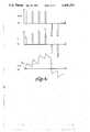
- FIG. 4shows the voltage waveform for a selected pel, (FIG. 4, waveform a), together with the corresponding variation of current I through a switch, (FIG. 4, waveform b), and the voltage applied across the LC (FIG. 4, waveform c), all as a function of time.
- a current pulse directed through the MIM switchdecays as the LCD pel charges, so reducing the voltage across the switch.
- the currentdoes not reach a stable output value until a number of consecutive unipolar pulses of the waveform have been applied.
- the switch transient effectsif pulse polarity is reversed after every pulse, the current through the switch never reaches a stable value. In effect, using such an addressing scheme for a switched matrix multiplexed LCD of this type, the display is never fully turned on.
- the pel voltagereaches a value V th at which the display is fully turned on.
- the current decay timeincreases with increasing LC pel capacitance.
- the voltage across the LC peldepends on the difference between the charging and discharging time constants of the LC.
- the transient effect of MIM switchesoccurs, it is thought, owing to the time taken for the establishment of equilibrium between current carrier trapping and de-trapping rates in the thin film MIM switch. Other mechanisms may also be responsible for this effect.
- the rate of polarity reversalmust be greater than 30 Hz which is the flicker fusion rate.
- the number of pulses between polarity reversalsis limited by the number of lines being multiplexed.
Landscapes
- Physics & Mathematics (AREA)
- Engineering & Computer Science (AREA)
- Chemical & Material Sciences (AREA)
- Crystallography & Structural Chemistry (AREA)
- General Physics & Mathematics (AREA)
- Nonlinear Science (AREA)
- Computer Hardware Design (AREA)
- Theoretical Computer Science (AREA)
- Microelectronics & Electronic Packaging (AREA)
- Mathematical Physics (AREA)
- Optics & Photonics (AREA)
- Liquid Crystal Display Device Control (AREA)
Abstract
Description
Claims (6)
Priority Applications (1)
| Application Number | Priority Date | Filing Date | Title |
|---|---|---|---|
| US06/271,973US4404555A (en) | 1981-06-09 | 1981-06-09 | Addressing scheme for switch controlled liquid crystal displays |
Applications Claiming Priority (1)
| Application Number | Priority Date | Filing Date | Title |
|---|---|---|---|
| US06/271,973US4404555A (en) | 1981-06-09 | 1981-06-09 | Addressing scheme for switch controlled liquid crystal displays |
Publications (1)
| Publication Number | Publication Date |
|---|---|
| US4404555Atrue US4404555A (en) | 1983-09-13 |
Family
ID=23037873
Family Applications (1)
| Application Number | Title | Priority Date | Filing Date |
|---|---|---|---|
| US06/271,973Expired - LifetimeUS4404555A (en) | 1981-06-09 | 1981-06-09 | Addressing scheme for switch controlled liquid crystal displays |
Country Status (1)
| Country | Link |
|---|---|
| US (1) | US4404555A (en) |
Cited By (24)
| Publication number | Priority date | Publication date | Assignee | Title |
|---|---|---|---|---|
| US4525710A (en)* | 1982-02-16 | 1985-06-25 | Seiko Instruments & Electronics Ltd. | Picture display device |
| EP0174431A1 (en)* | 1984-09-10 | 1986-03-19 | International Business Machines Corporation | Liquid crystal display devices and method for production thereof |
| US4586039A (en)* | 1982-04-26 | 1986-04-29 | Sharp Kabushiki Kaisha | Liquid crystal display device and method for driving thereof |
| US4604617A (en)* | 1982-08-23 | 1986-08-05 | Seiko Epson Corporation | Driving system for a matrix display panel |
| WO1986005003A1 (en)* | 1985-02-25 | 1986-08-28 | American Telephone & Telegraph Company | Temperature compensation in active substrate electro-optic displays |
| US4638310A (en)* | 1983-09-10 | 1987-01-20 | International Standard Electric Company | Method of addressing liquid crystal displays |
| US4698668A (en)* | 1982-08-30 | 1987-10-06 | Canadian Industrial Innovation Centre/Waterloo | Apparatus for influencing the presentation of visual information |
| US4701025A (en)* | 1984-08-20 | 1987-10-20 | Hitachi, Ltd. | Liquid crystal display device with driving method to eliminate blur due to frequency dependence |
| US4705345A (en)* | 1985-04-03 | 1987-11-10 | Stc Plc | Addressing liquid crystal cells using unipolar strobe pulses |
| US4722594A (en)* | 1984-11-14 | 1988-02-02 | Stc Plc | Two-dimensional optical information processing apparatus |
| US4728947A (en)* | 1985-04-03 | 1988-03-01 | Stc Plc | Addressing liquid crystal cells using bipolar data strobe pulses |
| US4783653A (en)* | 1985-11-04 | 1988-11-08 | U.S. Philips Corporation | Low drive voltage display device |
| EP0211599A3 (en)* | 1985-08-02 | 1989-02-22 | Hitachi, Ltd. | Liquid crystal display device |
| US4818981A (en)* | 1986-09-11 | 1989-04-04 | Fujitsu Limited | Active matrix display device and method for driving the same |
| US4990905A (en)* | 1986-07-10 | 1991-02-05 | U.S. Philips Corp. | Method of driving a display device and a display device suitable for such method |
| US5247376A (en)* | 1988-11-17 | 1993-09-21 | Seiko Epson Corporation | Method of driving a liquid crystal display device |
| US5448383A (en)* | 1983-04-19 | 1995-09-05 | Canon Kabushiki Kaisha | Method of driving ferroelectric liquid crystal optical modulation device |
| US5666133A (en)* | 1991-12-13 | 1997-09-09 | Kyocera Corporation | Method for driving liquid crystal display unit |
| US6023256A (en)* | 1996-05-15 | 2000-02-08 | Motorola, Inc. | Liquid crystal display driver system and method therefor |
| US6128050A (en)* | 1994-11-08 | 2000-10-03 | Citizen Watch Co., Ltd. | Liquid crystal display device with separated anode oxide electrode |
| US6816138B2 (en) | 2000-04-27 | 2004-11-09 | Manning Ventures, Inc. | Graphic controller for active matrix addressed bistable reflective cholesteric displays |
| US6819310B2 (en) | 2000-04-27 | 2004-11-16 | Manning Ventures, Inc. | Active matrix addressed bistable reflective cholesteric displays |
| US6850217B2 (en) | 2000-04-27 | 2005-02-01 | Manning Ventures, Inc. | Operating method for active matrix addressed bistable reflective cholesteric displays |
| US20060103641A1 (en)* | 2004-11-12 | 2006-05-18 | Kent Displays Incorporated | Display device with electrical zipper interconnect |
Citations (3)
| Publication number | Priority date | Publication date | Assignee | Title |
|---|---|---|---|---|
| US3809458A (en)* | 1972-05-25 | 1974-05-07 | Rca Corp | Liquid crystal display |
| US3895372A (en)* | 1973-01-24 | 1975-07-15 | Hitachi Ltd | Quick response liquid crystal display device |
| US4223308A (en)* | 1979-07-25 | 1980-09-16 | Northern Telecom Limited | LCDs (Liquid crystal displays) controlled by thin film diode switches |
- 1981
- 1981-06-09USUS06/271,973patent/US4404555A/ennot_activeExpired - Lifetime
Patent Citations (3)
| Publication number | Priority date | Publication date | Assignee | Title |
|---|---|---|---|---|
| US3809458A (en)* | 1972-05-25 | 1974-05-07 | Rca Corp | Liquid crystal display |
| US3895372A (en)* | 1973-01-24 | 1975-07-15 | Hitachi Ltd | Quick response liquid crystal display device |
| US4223308A (en)* | 1979-07-25 | 1980-09-16 | Northern Telecom Limited | LCDs (Liquid crystal displays) controlled by thin film diode switches |
Cited By (44)
| Publication number | Priority date | Publication date | Assignee | Title |
|---|---|---|---|---|
| US4525710A (en)* | 1982-02-16 | 1985-06-25 | Seiko Instruments & Electronics Ltd. | Picture display device |
| US4586039A (en)* | 1982-04-26 | 1986-04-29 | Sharp Kabushiki Kaisha | Liquid crystal display device and method for driving thereof |
| US4604617A (en)* | 1982-08-23 | 1986-08-05 | Seiko Epson Corporation | Driving system for a matrix display panel |
| US4698668A (en)* | 1982-08-30 | 1987-10-06 | Canadian Industrial Innovation Centre/Waterloo | Apparatus for influencing the presentation of visual information |
| US6091388A (en)* | 1983-04-13 | 2000-07-18 | Canon Kabushiki Kaisha | Method of driving optical modulation device |
| US5565884A (en)* | 1983-04-19 | 1996-10-15 | Canon Kabushiki Kaisha | Method of driving optical modulation device |
| US5696525A (en)* | 1983-04-19 | 1997-12-09 | Canon Kabushiki Kaisha | Method of driving optical modulation device |
| US5790449A (en)* | 1983-04-19 | 1998-08-04 | Canon Kabushiki Kaisha | Method of driving optical modulation device |
| US5448383A (en)* | 1983-04-19 | 1995-09-05 | Canon Kabushiki Kaisha | Method of driving ferroelectric liquid crystal optical modulation device |
| US5621427A (en)* | 1983-04-19 | 1997-04-15 | Canon Kabushiki Kaisha | Method of driving optical modulation device |
| US5548303A (en)* | 1983-04-19 | 1996-08-20 | Canon Kabushiki Kaisha | Method of driving optical modulation device |
| US5696526A (en)* | 1983-04-19 | 1997-12-09 | Canon Kabushiki Kaisha | Method of driving optical modulation device |
| US5592192A (en)* | 1983-04-19 | 1997-01-07 | Canon Kabushiki Kaisha | Method of driving optical modulation device |
| US5886680A (en)* | 1983-04-19 | 1999-03-23 | Canon Kabushiki Kaisha | Method of driving optical modulation device |
| US5841417A (en)* | 1983-04-19 | 1998-11-24 | Canon Kabushiki Kaisha | Method of driving optical modulation device |
| US5831587A (en)* | 1983-04-19 | 1998-11-03 | Canon Kabushiki Kaisha | Method of driving optical modulation device |
| US5825390A (en)* | 1983-04-19 | 1998-10-20 | Canon Kabushiki Kaisha | Method of driving optical modulation device |
| US5812108A (en)* | 1983-04-19 | 1998-09-22 | Canon Kabushiki Kaisha | Method of driving optical modulation device |
| US4638310A (en)* | 1983-09-10 | 1987-01-20 | International Standard Electric Company | Method of addressing liquid crystal displays |
| EP0173158A3 (en)* | 1984-08-20 | 1988-07-13 | Hitachi, Ltd. | Liquid crystal display device |
| US4701025A (en)* | 1984-08-20 | 1987-10-20 | Hitachi, Ltd. | Liquid crystal display device with driving method to eliminate blur due to frequency dependence |
| US4662719A (en)* | 1984-09-10 | 1987-05-05 | International Business Machines Corporation | Liquid crystal display and method for production |
| EP0174431A1 (en)* | 1984-09-10 | 1986-03-19 | International Business Machines Corporation | Liquid crystal display devices and method for production thereof |
| US4722594A (en)* | 1984-11-14 | 1988-02-02 | Stc Plc | Two-dimensional optical information processing apparatus |
| WO1986005003A1 (en)* | 1985-02-25 | 1986-08-28 | American Telephone & Telegraph Company | Temperature compensation in active substrate electro-optic displays |
| US4728947A (en)* | 1985-04-03 | 1988-03-01 | Stc Plc | Addressing liquid crystal cells using bipolar data strobe pulses |
| US4705345A (en)* | 1985-04-03 | 1987-11-10 | Stc Plc | Addressing liquid crystal cells using unipolar strobe pulses |
| EP0197742A3 (en)* | 1985-04-03 | 1989-03-01 | International Standard Electric Corporation | Addressing liquid crystal cells |
| EP0211599A3 (en)* | 1985-08-02 | 1989-02-22 | Hitachi, Ltd. | Liquid crystal display device |
| US4783653A (en)* | 1985-11-04 | 1988-11-08 | U.S. Philips Corporation | Low drive voltage display device |
| US4990905A (en)* | 1986-07-10 | 1991-02-05 | U.S. Philips Corp. | Method of driving a display device and a display device suitable for such method |
| US4818981A (en)* | 1986-09-11 | 1989-04-04 | Fujitsu Limited | Active matrix display device and method for driving the same |
| US5247376A (en)* | 1988-11-17 | 1993-09-21 | Seiko Epson Corporation | Method of driving a liquid crystal display device |
| US5666133A (en)* | 1991-12-13 | 1997-09-09 | Kyocera Corporation | Method for driving liquid crystal display unit |
| US6388720B1 (en) | 1994-11-08 | 2002-05-14 | Citizen Watch Co., Ltd. | Liquid crystal display including signal electrodes connected to each other by first anode oxide electrode and auxiliary electrode connected to second anode oxide electrode |
| US6128050A (en)* | 1994-11-08 | 2000-10-03 | Citizen Watch Co., Ltd. | Liquid crystal display device with separated anode oxide electrode |
| US6023256A (en)* | 1996-05-15 | 2000-02-08 | Motorola, Inc. | Liquid crystal display driver system and method therefor |
| US6816138B2 (en) | 2000-04-27 | 2004-11-09 | Manning Ventures, Inc. | Graphic controller for active matrix addressed bistable reflective cholesteric displays |
| US6819310B2 (en) | 2000-04-27 | 2004-11-16 | Manning Ventures, Inc. | Active matrix addressed bistable reflective cholesteric displays |
| US6850217B2 (en) | 2000-04-27 | 2005-02-01 | Manning Ventures, Inc. | Operating method for active matrix addressed bistable reflective cholesteric displays |
| US20050083284A1 (en)* | 2000-04-27 | 2005-04-21 | Manning Ventures-Inc. | Graphic controller for active matrix addressed bistable reflective Cholesteric displays |
| US7317437B2 (en) | 2000-04-27 | 2008-01-08 | Manning Ventures, Inc. | Graphic controller for active matrix addressed bistable reflective Cholesteric displays |
| US20060103641A1 (en)* | 2004-11-12 | 2006-05-18 | Kent Displays Incorporated | Display device with electrical zipper interconnect |
| US7479940B2 (en) | 2004-11-12 | 2009-01-20 | Kent Displays Incorporated | Display device with electrical zipper interconnect |
Similar Documents
| Publication | Publication Date | Title |
|---|---|---|
| US4404555A (en) | Addressing scheme for switch controlled liquid crystal displays | |
| US6335717B2 (en) | Liquid crystal display device | |
| US5898416A (en) | Display device | |
| US4528562A (en) | Co-ordinate addressing of smectic display cells | |
| JP2505826B2 (en) | Display device | |
| US4763994A (en) | Method and apparatus for driving ferroelectric liquid crystal optical modulation device | |
| CN88101453A (en) | Liquid crystal display device and driving method thereof | |
| JPH04269792A (en) | Driving method for matrix display apparatus and matrix display apparatus which can be operated by this method | |
| GB2324899A (en) | Active matrix display | |
| KR960008099B1 (en) | Matrix display device | |
| US6320571B1 (en) | Bistable liquid crystal display device | |
| KR960007476B1 (en) | Display device and driving method thereof | |
| US4746196A (en) | Multiplexed driving method for an optical switching element employing ferroelectric liquid crystal | |
| JP5148048B2 (en) | Bistable nematic liquid crystal display device and method for controlling such a device | |
| KR20020095167A (en) | Bistable chiral nematic liquid crystal display and method of driving the same | |
| US5032830A (en) | Electro-optical display device with non-linear switching units with auxiliary voltages and capacitively coupled row electrodes | |
| EP0175417B1 (en) | Liquid crystal display device | |
| KR930010835A (en) | Driving Method of Liquid Crystal Panel | |
| CA1184681A (en) | Addressing scheme for switch controlled liquid crystal displays | |
| US4116543A (en) | Control electro-optical device utilizing liquid crystal | |
| US4783653A (en) | Low drive voltage display device | |
| KR100296835B1 (en) | Addressed ferroelectric liquid crystal display | |
| KR100324438B1 (en) | Liquid crystal device and method of addressing liquid crystal device | |
| US6046715A (en) | Liquid crystal array device | |
| US20030122768A1 (en) | Antiferroelectric liquid crystal devices |
Legal Events
| Date | Code | Title | Description |
|---|---|---|---|
| AS | Assignment | Owner name:NORTHERN TELECOM LIMITED, P.O. BOX 6123, MONTREAL, Free format text:ASSIGNMENT OF ASSIGNORS INTEREST.;ASSIGNOR:BELL-NORTHERN RESEARCH, LTD.,;REEL/FRAME:003902/0130 Effective date:19810601 Owner name:BELL-NORTHERN RESEARCH LTD., P.O. BOX 3511, STATIO Free format text:ASSIGNMENT OF ASSIGNORS INTEREST.;ASSIGNORS:LONG, JOHN R.;MINER, CARLA J.;STREATER, RICHARD W.;AND OTHERS;REEL/FRAME:003902/0129 Effective date:19810601 | |
| STCF | Information on status: patent grant | Free format text:PATENTED CASE | |
| MAFP | Maintenance fee payment | Free format text:PAYMENT OF MAINTENANCE FEE, 4TH YEAR, PL 96-517 (ORIGINAL EVENT CODE: M170); ENTITY STATUS OF PATENT OWNER: LARGE ENTITY Year of fee payment:4 | |
| FEPP | Fee payment procedure | Free format text:PAYOR NUMBER ASSIGNED (ORIGINAL EVENT CODE: ASPN); ENTITY STATUS OF PATENT OWNER: LARGE ENTITY | |
| MAFP | Maintenance fee payment | Free format text:PAYMENT OF MAINTENANCE FEE, 8TH YEAR, PL 96-517 (ORIGINAL EVENT CODE: M171); ENTITY STATUS OF PATENT OWNER: LARGE ENTITY Year of fee payment:8 | |
| MAFP | Maintenance fee payment | Free format text:PAYMENT OF MAINTENANCE FEE, 12TH YEAR, LARGE ENTITY (ORIGINAL EVENT CODE: M185); ENTITY STATUS OF PATENT OWNER: LARGE ENTITY Year of fee payment:12 | |
| AS | Assignment | Owner name:NORTEL NETWORKS CORPORATION, CANADA Free format text:CHANGE OF NAME;ASSIGNOR:NORTHERN TELECOM LIMITED;REEL/FRAME:010567/0001 Effective date:19990429 | |
| AS | Assignment | Owner name:NORTEL NETWORKS LIMITED, CANADA Free format text:CHANGE OF NAME;ASSIGNOR:NORTEL NETWORKS CORPORATION;REEL/FRAME:011195/0706 Effective date:20000830 Owner name:NORTEL NETWORKS LIMITED,CANADA Free format text:CHANGE OF NAME;ASSIGNOR:NORTEL NETWORKS CORPORATION;REEL/FRAME:011195/0706 Effective date:20000830 |