US4403238A - Detector array focal plane configuration - Google Patents
Detector array focal plane configurationDownload PDFInfo
- Publication number
- US4403238A US4403238AUS06/213,933US21393380AUS4403238AUS 4403238 AUS4403238 AUS 4403238AUS 21393380 AUS21393380 AUS 21393380AUS 4403238 AUS4403238 AUS 4403238A
- Authority
- US
- United States
- Prior art keywords
- photo
- focal plane
- electrical contact
- center
- detectors
- Prior art date
- Legal status (The legal status is an assumption and is not a legal conclusion. Google has not performed a legal analysis and makes no representation as to the accuracy of the status listed.)
- Expired - Lifetime
Links
Images


Classifications
- H—ELECTRICITY
- H01—ELECTRIC ELEMENTS
- H01L—SEMICONDUCTOR DEVICES NOT COVERED BY CLASS H10
- H01L25/00—Assemblies consisting of a plurality of semiconductor or other solid state devices
- H01L25/03—Assemblies consisting of a plurality of semiconductor or other solid state devices all the devices being of a type provided for in a single subclass of subclasses H10B, H10D, H10F, H10H, H10K or H10N, e.g. assemblies of rectifier diodes
- H01L25/04—Assemblies consisting of a plurality of semiconductor or other solid state devices all the devices being of a type provided for in a single subclass of subclasses H10B, H10D, H10F, H10H, H10K or H10N, e.g. assemblies of rectifier diodes the devices not having separate containers
- H01L25/041—Assemblies consisting of a plurality of semiconductor or other solid state devices all the devices being of a type provided for in a single subclass of subclasses H10B, H10D, H10F, H10H, H10K or H10N, e.g. assemblies of rectifier diodes the devices not having separate containers the devices being of a type provided for in subclass H10F
- H01L25/043—Stacked arrangements of devices
- H—ELECTRICITY
- H10—SEMICONDUCTOR DEVICES; ELECTRIC SOLID-STATE DEVICES NOT OTHERWISE PROVIDED FOR
- H10F—INORGANIC SEMICONDUCTOR DEVICES SENSITIVE TO INFRARED RADIATION, LIGHT, ELECTROMAGNETIC RADIATION OF SHORTER WAVELENGTH OR CORPUSCULAR RADIATION
- H10F39/00—Integrated devices, or assemblies of multiple devices, comprising at least one element covered by group H10F30/00, e.g. radiation detectors comprising photodiode arrays
- H10F39/10—Integrated devices
- H10F39/107—Integrated devices having multiple elements covered by H10F30/00 in a repetitive configuration, e.g. radiation detectors comprising photodiode arrays
- H—ELECTRICITY
- H01—ELECTRIC ELEMENTS
- H01L—SEMICONDUCTOR DEVICES NOT COVERED BY CLASS H10
- H01L2924/00—Indexing scheme for arrangements or methods for connecting or disconnecting semiconductor or solid-state bodies as covered by H01L24/00
- H01L2924/0001—Technical content checked by a classifier
- H01L2924/0002—Not covered by any one of groups H01L24/00, H01L24/00 and H01L2224/00
Definitions
- This inventionrelates to the field of electro-optical detecting apparatus which utilizes "mosaic" detector arrays to provide surveillance of an extensive scene.
- the mosaic detector arraysare large numbers of closely spaced individual photodetector elements arranged in essentially a two-dimensional, or planar, array.
- a detector array modulewhich comprises a stack of semiconductor chips, or layers, extending at right angles to the focal plane of the detector array, which array comprises a multiplicity of separate photo-detectors each in electrical contact with a single electrical lead formed as one of a multiplicity of such leads which appear on the focal plane ends of the stacked chips.
- Each of the chipsas integrated electronic circuitry which processes signals from the detectors prior to transmitting output signals to electronic processing circuits located remote from the focal plane assembly.
- the complete focal plane assemblyis constructed by combining a large number of the modules.
- the goal of such structuresis to derive individual detector signals from photo-detectors which have a very small center-to-center distance, in order to provide optimum resolution of the incoming optical information.
- the desired spacing of the detectorsis determined by the size of the optics system in the sensor. Longer focal lengths in the optics system permit greater spacing of the detectors. There is a design trade-off between the dimensions of the focal plane and the optics, on the one hand, and the size and spacing of the detectors, on the other hand.
- Compact optical receiving systemsrequire small, closely spaced detectors. Except for the diffraction limit, the desire is to increase to the maximum the number of individual detectors in a given focal plane area. It is desirable to obtain the smallest possible F-number, which is the ratio of focal length of the optics to the diameter of the input aperture.
- the ideal center-to-center detector distanceis about 1.5 mils; and for infra-red radiation in the 3-5 micron range, with an F/no. of 1.5, the ideal center-to-center detector distance is about 0.75 mil. In units presently under development, the minimum distance is about 4 mils.
- the primary deterrent to reducing the distanceis the required thickness of each layer. If the layers are too thin, they will be very fragile, and will therefore be extremely difficult to handle during fabrication of the multi-layer modules.
- the problem of layer fragilityis, in fact, a significant one where a 4 mil dimension is used.
- the purpose of the present inventionis to significantly improve the strength of the layers and/or the closeness of the detector centers. In other words, the goal is to make it possible to bring the detectors closer together, given the limitation imposed by the strength requirement of the layers.
- the present inventionaccomplishes the foregoing purpose by orienting the detector rows along lines which extend diagonally with respect to the planes in which the layers extend, thereby permitting the distance between adjacent detector rows to be less than the thickness of a given layer.
- This benefitcan be used to reduce fragility of the layers, or to reduce the distance between detectors, or to obtain a combination of those advantages.
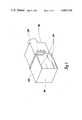
- FIGS. 1 and 2are substantially identical to the correspondingly numbered figures in application Ser. No. 187,787, FIG. 1 showing in perspective an assembled module comprising a number of stacked layers, and FIG. 2 being a partially exploded view of the same module;
- FIG. 3is a closeup view of the electrical leads which extend to the focal plane of the module
- FIG. 4is a closeup view, similar to FIG. 3, showing the positions of the photo-detectors on top of the module in individual electrical contact with the respective leads;
- FIG. 5is a cross-sectional view taken on the line 5--5 of FIG. 4.
- the modulecomprises a stack of silicon (semiconductor) chips. It should be understood, however, that the concept disclosed in the present application is also applicable to any detector array module which comprises stacked layers extending in planes which are perpendicular to the focal plane, such as the structure disclosed in Carson and Dahlgren application Ser. No. 855,242, filed Nov. 28, 1977.
- FIG. 1shows a module 12 comprising a multiplicity of layers 14, each of which is a semiconductor chip (preferably silicon) which carries an integrated circuit having suitable electrical leads terminating at a front, or focal, plane 16, where they are individually in electrical contact with separate very closely spaced photo-detectors.
- the module 12is in effect, a stack, or "sandwich,” comprising numerous silicon chips, or substrates, secured together by suitable adhesive material between adjacent chips.
- the stack of chipsis mounted on a supporting block 18, which also functions as a heat-transfer, or cooling, structure, and which may have a mounting stud 20 for use in securing the module and its supporting block in a larger assembly.
- a module assemblyGenerally the combination of the stack of silicon chips and the supporting block is considered to be a module assembly.
- FIG. 2is an exploded view of module 12, it is seen that it includes separately formed silicon chips 14 which, after being stacked and glued together, are provided on the front, or focal, plane with a detector "mosaic" 28 and on the rear, or back, plane with back plane wiring 30.
- the supporting block 18is preferably molybdenum, selected because of its thermal compatibility with silicon. It is insulated from the back plane of the silicon substrate stack by a flat insulating board 32, preferably formed of silicon having silicon oxide grown or deposited on its surfaces.
- Two additional insulating boards 34 and 36, also preferably formed of silicon,are secured to two sides of molybdenum block 18, and are arranged to carry lead-out conductors from the back plane wiring 30 to ribbon cables (not shown).
- FIG. 3is a closeup of a small portion of the focal plane showing the spatial relationship of a number of electrical leads which intersect the focal plane.
- a surface 40 of each of the silicon chip layers 14carries thereon a multiplicity of closely spaced electrical leads 42, each of which is electrically isolated from all the others.
- the leadsbecause they have been deposited as thin film strips on the surface of each layer, will normally have a width of approximately 0.0005 to 0.001 inch and a thickness of approximately 10,000 A°. It will be noted that the spacing between adjacent leads on a given layer is substantially smaller than the thickness of each layer. If we assume a layer thickness of approximately 0.0028 inch, the center-to-center distance between adjacent leads on the same layer will be about 0.0014 inch. The reason for this 2 to 1 ratio of layer thickness to spacing of adjacent leads is the novel detector arrangement discussed below.
- FIGS. 4 and 5show the photo-detectors in place on top of the focal plane.
- Each photo-detector 44is spaced from adjacent photo-detectors by channels 46, thereby isolating the individual photo-detectors electrically.
- the center-to-center spacing between adjacent photo-detectorsshould be the same throughout the area of the focal plane.
- the photo-detectorswhich are preferably essentially square in shape, as shown, are arranged in rows which extend diagonally across the focal plane. In other words, the rows of photo-detectors are at 45° angles with respect to the planes in which the layers 14 extend. As a result of this diagonal relationship, the thickness of each layer is substantially equal to the diagonal of a square having its side equal to the distance between the centers of adjacent detectors.
- the center-to-center distance between adjacent detectors 44is substantially less than the thickness of the layers 14.
- Each layerhas a thickness equal to 1.414 ( ⁇ 2) times the detector distance.
- this spatial relationshipcan be used either to reduce the detector distance, or to increase the layer thickness, or to provide a combination of those two design changes.
- the detector center-to-center spacingwould be about 0.002 inch.
- the same ratioapplies to the spacing of the detectors and the lateral spacing of the leads, the former being 1.414 ( ⁇ 2) times the latter. So, as already stated, the centers of adjacent leads on the same layer would be spaced about 0.0014 inch if the detector centers are about 0.002 inch apart.
- each electrical lead 42makes contact with its detector 44 near one corner of the detector. This requires extreme accuracy of detector placement, such as that provided by the process disclosed in Rotolante and Koehler application Ser. No. 15,070, filed Feb. 26, 1979.
- each photo-detector 44may be electrically isolated from all other photo-detectors by means of a process which cuts the channels 46 through both a wafer of detector material and an initial uninterrupted layer of conductive epoxy.
Landscapes
- Engineering & Computer Science (AREA)
- Power Engineering (AREA)
- Microelectronics & Electronic Packaging (AREA)
- Physics & Mathematics (AREA)
- Condensed Matter Physics & Semiconductors (AREA)
- General Physics & Mathematics (AREA)
- Computer Hardware Design (AREA)
- Solid State Image Pick-Up Elements (AREA)
Abstract
Description
Claims (10)
Priority Applications (1)
| Application Number | Priority Date | Filing Date | Title |
|---|---|---|---|
| US06/213,933US4403238A (en) | 1980-12-08 | 1980-12-08 | Detector array focal plane configuration |
Applications Claiming Priority (1)
| Application Number | Priority Date | Filing Date | Title |
|---|---|---|---|
| US06/213,933US4403238A (en) | 1980-12-08 | 1980-12-08 | Detector array focal plane configuration |
Publications (1)
| Publication Number | Publication Date |
|---|---|
| US4403238Atrue US4403238A (en) | 1983-09-06 |
Family
ID=22797090
Family Applications (1)
| Application Number | Title | Priority Date | Filing Date |
|---|---|---|---|
| US06/213,933Expired - LifetimeUS4403238A (en) | 1980-12-08 | 1980-12-08 | Detector array focal plane configuration |
Country Status (1)
| Country | Link |
|---|---|
| US (1) | US4403238A (en) |
Cited By (22)
| Publication number | Priority date | Publication date | Assignee | Title |
|---|---|---|---|---|
| US4575762A (en)* | 1983-09-12 | 1986-03-11 | Rockwell International Corporation | Integrated processor board assembly |
| US4703170A (en)* | 1985-04-12 | 1987-10-27 | Grumman Aerospace Corporation | Infrared focal plane module |
| US4792672A (en)* | 1985-04-12 | 1988-12-20 | Grumman Aerospace Corporation | Detector buffer board |
| US4794092A (en)* | 1987-11-18 | 1988-12-27 | Grumman Aerospace Corporation | Single wafer moated process |
| US4927771A (en)* | 1989-03-07 | 1990-05-22 | The United States Of America As Represented By The Secretary Of The Army | Method of thermal isolation of detector elements in an uncooled staring focal plane array |
| US5093708A (en)* | 1990-08-20 | 1992-03-03 | Grumman Aerospace Corporation | Multilayer integrated circuit module |
| US5128749A (en)* | 1991-04-08 | 1992-07-07 | Grumman Aerospace Corporation | Fused high density multi-layer integrated circuit module |
| US5209798A (en)* | 1991-11-22 | 1993-05-11 | Grunman Aerospace Corporation | Method of forming a precisely spaced stack of substrate layers |
| US5231304A (en)* | 1989-07-27 | 1993-07-27 | Grumman Aerospace Corporation | Framed chip hybrid stacked layer assembly |
| US5379191A (en)* | 1991-02-26 | 1995-01-03 | Microelectronics And Computer Technology Corporation | Compact adapter package providing peripheral to area translation for an integrated circuit chip |
| US5479015A (en)* | 1994-08-18 | 1995-12-26 | Grumman Aerospace Corporation | Multi-image detector assembly |
| US5493096A (en)* | 1994-05-10 | 1996-02-20 | Grumman Aerospace Corporation | Thin substrate micro-via interconnect |
| US5621193A (en)* | 1995-05-23 | 1997-04-15 | Northrop Grumman Corporation | Ceramic edge connect process |
| US5712747A (en)* | 1996-01-24 | 1998-01-27 | International Business Machines Corporation | Thin film slider with on-board multi-layer integrated circuit |
| US5763943A (en)* | 1996-01-29 | 1998-06-09 | International Business Machines Corporation | Electronic modules with integral sensor arrays |
| US5856235A (en)* | 1995-04-12 | 1999-01-05 | Northrop Grumman Corporation | Process of vacuum annealing a thin film metallization on high purity alumina |
| US20030036218A1 (en)* | 2001-08-17 | 2003-02-20 | Farrar Paul A. | Three-dimensional multichip module |
| US20030192171A1 (en)* | 2002-01-16 | 2003-10-16 | Fey Kate E. | Space-saving packaging of electronic circuits |
| US20040207061A1 (en)* | 2001-08-30 | 2004-10-21 | Farrar Paul A. | Multi-chip electronic package and cooling system |
| US20060126307A1 (en)* | 2003-12-04 | 2006-06-15 | Albert Douglas | Cornerbond assembly comprising three-dimensional electronic modules |
| US7772045B1 (en) | 2006-10-24 | 2010-08-10 | Randy Wayne Bindrup | Wire bond method for angularly disposed conductive pads and a device made from the method |
| US10916524B2 (en)* | 2016-12-29 | 2021-02-09 | Intel Corporation | Stacked dice systems |
Citations (1)
| Publication number | Priority date | Publication date | Assignee | Title |
|---|---|---|---|---|
| US3852714A (en)* | 1972-06-22 | 1974-12-03 | Eocom Corp | Adaptive imaging system |
- 1980
- 1980-12-08USUS06/213,933patent/US4403238A/ennot_activeExpired - Lifetime
Patent Citations (1)
| Publication number | Priority date | Publication date | Assignee | Title |
|---|---|---|---|---|
| US3852714A (en)* | 1972-06-22 | 1974-12-03 | Eocom Corp | Adaptive imaging system |
Cited By (31)
| Publication number | Priority date | Publication date | Assignee | Title |
|---|---|---|---|---|
| US4575762A (en)* | 1983-09-12 | 1986-03-11 | Rockwell International Corporation | Integrated processor board assembly |
| US4703170A (en)* | 1985-04-12 | 1987-10-27 | Grumman Aerospace Corporation | Infrared focal plane module |
| US4792672A (en)* | 1985-04-12 | 1988-12-20 | Grumman Aerospace Corporation | Detector buffer board |
| US4794092A (en)* | 1987-11-18 | 1988-12-27 | Grumman Aerospace Corporation | Single wafer moated process |
| US4927771A (en)* | 1989-03-07 | 1990-05-22 | The United States Of America As Represented By The Secretary Of The Army | Method of thermal isolation of detector elements in an uncooled staring focal plane array |
| US5231304A (en)* | 1989-07-27 | 1993-07-27 | Grumman Aerospace Corporation | Framed chip hybrid stacked layer assembly |
| US5093708A (en)* | 1990-08-20 | 1992-03-03 | Grumman Aerospace Corporation | Multilayer integrated circuit module |
| US5379191A (en)* | 1991-02-26 | 1995-01-03 | Microelectronics And Computer Technology Corporation | Compact adapter package providing peripheral to area translation for an integrated circuit chip |
| US5128749A (en)* | 1991-04-08 | 1992-07-07 | Grumman Aerospace Corporation | Fused high density multi-layer integrated circuit module |
| US5209798A (en)* | 1991-11-22 | 1993-05-11 | Grunman Aerospace Corporation | Method of forming a precisely spaced stack of substrate layers |
| US5493096A (en)* | 1994-05-10 | 1996-02-20 | Grumman Aerospace Corporation | Thin substrate micro-via interconnect |
| US5479015A (en)* | 1994-08-18 | 1995-12-26 | Grumman Aerospace Corporation | Multi-image detector assembly |
| US5856235A (en)* | 1995-04-12 | 1999-01-05 | Northrop Grumman Corporation | Process of vacuum annealing a thin film metallization on high purity alumina |
| US5621193A (en)* | 1995-05-23 | 1997-04-15 | Northrop Grumman Corporation | Ceramic edge connect process |
| US5712747A (en)* | 1996-01-24 | 1998-01-27 | International Business Machines Corporation | Thin film slider with on-board multi-layer integrated circuit |
| US5771571A (en)* | 1996-01-24 | 1998-06-30 | International Business Machines Corporation | Method for manufacturing thin film slider with on-board multi-layer integrated circuit |
| US5763943A (en)* | 1996-01-29 | 1998-06-09 | International Business Machines Corporation | Electronic modules with integral sensor arrays |
| US5907178A (en)* | 1996-01-29 | 1999-05-25 | International Business Machines Corporation | Multi-view imaging apparatus |
| US5869896A (en)* | 1996-01-29 | 1999-02-09 | International Business Machines Corporation | Packaged electronic module and integral sensor array |
| US7465608B1 (en) | 2001-08-17 | 2008-12-16 | Micron Technology, Inc. | Three-dimensional multichip module |
| US20030036218A1 (en)* | 2001-08-17 | 2003-02-20 | Farrar Paul A. | Three-dimensional multichip module |
| US6790702B2 (en)* | 2001-08-17 | 2004-09-14 | Micron Technology, Inc. | Three-dimensional multichip module |
| US20040207061A1 (en)* | 2001-08-30 | 2004-10-21 | Farrar Paul A. | Multi-chip electronic package and cooling system |
| US6975027B2 (en) | 2001-08-30 | 2005-12-13 | Micron Technology, Inc. | Multi-chip electronic package and cooling system |
| US20060103015A1 (en)* | 2001-08-30 | 2006-05-18 | Farrar Paul A | Multi-chip electronic package and cooling system |
| US7626252B2 (en) | 2001-08-30 | 2009-12-01 | Micron Technology, Inc. | Multi-chip electronic package and cooling system |
| US20030192171A1 (en)* | 2002-01-16 | 2003-10-16 | Fey Kate E. | Space-saving packaging of electronic circuits |
| US7071546B2 (en) | 2002-01-16 | 2006-07-04 | Alfred E. Mann Foundation For Scientific Research | Space-saving packaging of electronic circuits |
| US20060126307A1 (en)* | 2003-12-04 | 2006-06-15 | Albert Douglas | Cornerbond assembly comprising three-dimensional electronic modules |
| US7772045B1 (en) | 2006-10-24 | 2010-08-10 | Randy Wayne Bindrup | Wire bond method for angularly disposed conductive pads and a device made from the method |
| US10916524B2 (en)* | 2016-12-29 | 2021-02-09 | Intel Corporation | Stacked dice systems |
Similar Documents
| Publication | Publication Date | Title |
|---|---|---|
| US4403238A (en) | Detector array focal plane configuration | |
| US5737192A (en) | Density improvement in integration modules | |
| US4618763A (en) | Infrared focal plane module with stacked IC module body | |
| US4672737A (en) | Detector array module fabrication process | |
| US5135556A (en) | Method for making fused high density multi-layer integrated circuit module | |
| US4551629A (en) | Detector array module-structure and fabrication | |
| US5726500A (en) | Semiconductor hybrid component | |
| US4039833A (en) | High density infrared detector array | |
| US4659931A (en) | High density multi-layered integrated circuit package | |
| EP0317083B1 (en) | Single wafer moated signal processor | |
| EP0317084B1 (en) | Double wafer moated signal processor | |
| US4703170A (en) | Infrared focal plane module | |
| US4593456A (en) | Pyroelectric thermal detector array | |
| US4532424A (en) | Pyroelectric thermal detector array | |
| US4206470A (en) | Thin film interconnect for multicolor IR/CCD | |
| EP0161246B1 (en) | Detector array module-structure and fabrication | |
| US4575631A (en) | Infra-red detector | |
| US5064771A (en) | Method of forming crystal array | |
| JPH0370912B2 (en) | ||
| US5315147A (en) | Monolithic focal plane array | |
| US5432681A (en) | Density improvement for planar hybrid wafer scale integration | |
| US4354107A (en) | Detector array module-structure and fabrication | |
| US4283755A (en) | Modulator multilayer detector | |
| EP0308465B1 (en) | Detector buffer board | |
| US4352715A (en) | Detector array module fabrication |
Legal Events
| Date | Code | Title | Description |
|---|---|---|---|
| AS | Assignment | Owner name:IRVINE SENSORS CORPORATION A CA CORP. Free format text:ASSIGNMENT OF ASSIGNORS INTEREST.;ASSIGNOR:CLARK, STEWART A.;REEL/FRAME:004141/0954 Effective date:19830620 Owner name:IRVINE SENSORS CORPORATION, CALIFORNIA Free format text:ASSIGNMENT OF ASSIGNORS INTEREST;ASSIGNOR:CLARK, STEWART A.;REEL/FRAME:004141/0954 Effective date:19830620 | |
| STCF | Information on status: patent grant | Free format text:PATENTED CASE | |
| AS | Assignment | Owner name:SQUARE 1 BANK, NORTH CAROLINA Free format text:SECURITY INTEREST;ASSIGNOR:IRVINE SENSORS CORPORATION;REEL/FRAME:017435/0142 Effective date:20051230 | |
| AS | Assignment | Owner name:LONGVIEW FUND, L.P.,CALIFORNIA Free format text:SECURITY INTEREST;ASSIGNOR:IRVINE SENSORS CORP.;REEL/FRAME:018746/0842 Effective date:20061229 Owner name:ALPHA CAPITAL ANSTALT,LIECHTENSTEIN Free format text:SECURITY INTEREST;ASSIGNOR:IRVINE SENSORS CORP.;REEL/FRAME:018746/0842 Effective date:20061229 Owner name:ALPHA CAPITAL ANSTALT, LIECHTENSTEIN Free format text:SECURITY INTEREST;ASSIGNOR:IRVINE SENSORS CORP.;REEL/FRAME:018746/0842 Effective date:20061229 Owner name:LONGVIEW FUND, L.P., CALIFORNIA Free format text:SECURITY INTEREST;ASSIGNOR:IRVINE SENSORS CORP.;REEL/FRAME:018746/0842 Effective date:20061229 | |
| AS | Assignment | Owner name:ALPHA CAPITAL ANSTALT, LIECHTENSTEIN Free format text:SECURITY INTEREST;ASSIGNOR:IRVINE SENSORS CORP.;REEL/FRAME:018731/0600 Effective date:20061229 Owner name:LONGVIEW FUND, L.P., CALIFORNIA Free format text:SECURITY INTEREST;ASSIGNOR:IRVINE SENSORS CORP.;REEL/FRAME:018731/0600 Effective date:20061229 | |
| AS | Assignment | Owner name:IRVINE SENSORS CORPORATION, CALIFORNIA Free format text:SECURITY INTEREST;ASSIGNOR:SQUARE 1 BANK;REEL/FRAME:021861/0531 Effective date:20060929 | |
| AS | Assignment | Owner name:IRVINE SENSORS CORPORATION, CALIFORNIA Free format text:CORRECTION TO THE SECURITY INTEREST RELEASE EXECUTION DATE AND TYPOGRAPHICAL ERROR WHICH DESCRIBED THIS RELEASE AS A SECURITY AGREEMENT RATHER THAN AS A RELEASE OF SECURITY AGREEMENT AT REEL/FRAME 021861/0531 AND RECORDED ON 11/19/2008.;ASSIGNOR:SQUARE 1 BANK;REEL/FRAME:022137/0609 Effective date:20061229 | |
| AS | Assignment | Owner name:IRVINE SENSORS CORPORATION, CALIFORNIA Free format text:RELEASE BY SECURED PARTY;ASSIGNORS:LONGVIEW FUND, L.P.;ALPHA CAPITAL ANSTALT;REEL/FRAME:026632/0405 Effective date:20090227 |