US4403231A - Data recording medium - Google Patents
Data recording mediumDownload PDFInfo
- Publication number
- US4403231A US4403231AUS06/343,983US34398382AUS4403231AUS 4403231 AUS4403231 AUS 4403231AUS 34398382 AUS34398382 AUS 34398382AUS 4403231 AUS4403231 AUS 4403231A
- Authority
- US
- United States
- Prior art keywords
- recording medium
- layer
- data recording
- recording layer
- protective layer
- Prior art date
- Legal status (The legal status is an assumption and is not a legal conclusion. Google has not performed a legal analysis and makes no representation as to the accuracy of the status listed.)
- Expired - Fee Related
Links
Images
Classifications
- G—PHYSICS
- G11—INFORMATION STORAGE
- G11B—INFORMATION STORAGE BASED ON RELATIVE MOVEMENT BETWEEN RECORD CARRIER AND TRANSDUCER
- G11B7/00—Recording or reproducing by optical means, e.g. recording using a thermal beam of optical radiation by modifying optical properties or the physical structure, reproducing using an optical beam at lower power by sensing optical properties; Record carriers therefor
- G11B7/24—Record carriers characterised by shape, structure or physical properties, or by the selection of the material
- G11B7/26—Apparatus or processes specially adapted for the manufacture of record carriers
- G—PHYSICS
- G11—INFORMATION STORAGE
- G11B—INFORMATION STORAGE BASED ON RELATIVE MOVEMENT BETWEEN RECORD CARRIER AND TRANSDUCER
- G11B7/00—Recording or reproducing by optical means, e.g. recording using a thermal beam of optical radiation by modifying optical properties or the physical structure, reproducing using an optical beam at lower power by sensing optical properties; Record carriers therefor
- G11B7/24—Record carriers characterised by shape, structure or physical properties, or by the selection of the material
- G11B7/241—Record carriers characterised by shape, structure or physical properties, or by the selection of the material characterised by the selection of the material
- G11B7/252—Record carriers characterised by shape, structure or physical properties, or by the selection of the material characterised by the selection of the material of layers other than recording layers
- G11B7/254—Record carriers characterised by shape, structure or physical properties, or by the selection of the material characterised by the selection of the material of layers other than recording layers of protective topcoat layers
- G11B7/2542—Record carriers characterised by shape, structure or physical properties, or by the selection of the material characterised by the selection of the material of layers other than recording layers of protective topcoat layers consisting essentially of organic resins
- G—PHYSICS
- G11—INFORMATION STORAGE
- G11B—INFORMATION STORAGE BASED ON RELATIVE MOVEMENT BETWEEN RECORD CARRIER AND TRANSDUCER
- G11B7/00—Recording or reproducing by optical means, e.g. recording using a thermal beam of optical radiation by modifying optical properties or the physical structure, reproducing using an optical beam at lower power by sensing optical properties; Record carriers therefor
- G11B7/24—Record carriers characterised by shape, structure or physical properties, or by the selection of the material
- G11B7/241—Record carriers characterised by shape, structure or physical properties, or by the selection of the material characterised by the selection of the material
- G11B7/242—Record carriers characterised by shape, structure or physical properties, or by the selection of the material characterised by the selection of the material of recording layers
- G11B7/243—Record carriers characterised by shape, structure or physical properties, or by the selection of the material characterised by the selection of the material of recording layers comprising inorganic materials only, e.g. ablative layers
- G11B2007/24302—Metals or metalloids
- G11B2007/2431—Metals or metalloids group 13 elements (B, Al, Ga, In)
- G—PHYSICS
- G11—INFORMATION STORAGE
- G11B—INFORMATION STORAGE BASED ON RELATIVE MOVEMENT BETWEEN RECORD CARRIER AND TRANSDUCER
- G11B7/00—Recording or reproducing by optical means, e.g. recording using a thermal beam of optical radiation by modifying optical properties or the physical structure, reproducing using an optical beam at lower power by sensing optical properties; Record carriers therefor
- G11B7/24—Record carriers characterised by shape, structure or physical properties, or by the selection of the material
- G11B7/241—Record carriers characterised by shape, structure or physical properties, or by the selection of the material characterised by the selection of the material
- G11B7/242—Record carriers characterised by shape, structure or physical properties, or by the selection of the material characterised by the selection of the material of recording layers
- G11B7/243—Record carriers characterised by shape, structure or physical properties, or by the selection of the material characterised by the selection of the material of recording layers comprising inorganic materials only, e.g. ablative layers
- G11B2007/24302—Metals or metalloids
- G11B2007/24314—Metals or metalloids group 15 elements (e.g. Sb, Bi)
- G—PHYSICS
- G11—INFORMATION STORAGE
- G11B—INFORMATION STORAGE BASED ON RELATIVE MOVEMENT BETWEEN RECORD CARRIER AND TRANSDUCER
- G11B7/00—Recording or reproducing by optical means, e.g. recording using a thermal beam of optical radiation by modifying optical properties or the physical structure, reproducing using an optical beam at lower power by sensing optical properties; Record carriers therefor
- G11B7/24—Record carriers characterised by shape, structure or physical properties, or by the selection of the material
- G11B7/241—Record carriers characterised by shape, structure or physical properties, or by the selection of the material characterised by the selection of the material
- G11B7/242—Record carriers characterised by shape, structure or physical properties, or by the selection of the material characterised by the selection of the material of recording layers
- G11B7/243—Record carriers characterised by shape, structure or physical properties, or by the selection of the material characterised by the selection of the material of recording layers comprising inorganic materials only, e.g. ablative layers
- G11B2007/24302—Metals or metalloids
- G11B2007/24316—Metals or metalloids group 16 elements (i.e. chalcogenides, Se, Te)
- G—PHYSICS
- G11—INFORMATION STORAGE
- G11B—INFORMATION STORAGE BASED ON RELATIVE MOVEMENT BETWEEN RECORD CARRIER AND TRANSDUCER
- G11B7/00—Recording or reproducing by optical means, e.g. recording using a thermal beam of optical radiation by modifying optical properties or the physical structure, reproducing using an optical beam at lower power by sensing optical properties; Record carriers therefor
- G11B7/24—Record carriers characterised by shape, structure or physical properties, or by the selection of the material
- G11B7/241—Record carriers characterised by shape, structure or physical properties, or by the selection of the material characterised by the selection of the material
- G11B7/252—Record carriers characterised by shape, structure or physical properties, or by the selection of the material characterised by the selection of the material of layers other than recording layers
- G11B7/257—Record carriers characterised by shape, structure or physical properties, or by the selection of the material characterised by the selection of the material of layers other than recording layers of layers having properties involved in recording or reproduction, e.g. optical interference layers or sensitising layers or dielectric layers, which are protecting the recording layers
- G11B2007/25705—Record carriers characterised by shape, structure or physical properties, or by the selection of the material characterised by the selection of the material of layers other than recording layers of layers having properties involved in recording or reproduction, e.g. optical interference layers or sensitising layers or dielectric layers, which are protecting the recording layers consisting essentially of inorganic materials
- G11B2007/25706—Record carriers characterised by shape, structure or physical properties, or by the selection of the material characterised by the selection of the material of layers other than recording layers of layers having properties involved in recording or reproduction, e.g. optical interference layers or sensitising layers or dielectric layers, which are protecting the recording layers consisting essentially of inorganic materials containing transition metal elements (Zn, Fe, Co, Ni, Pt)
- G—PHYSICS
- G11—INFORMATION STORAGE
- G11B—INFORMATION STORAGE BASED ON RELATIVE MOVEMENT BETWEEN RECORD CARRIER AND TRANSDUCER
- G11B7/00—Recording or reproducing by optical means, e.g. recording using a thermal beam of optical radiation by modifying optical properties or the physical structure, reproducing using an optical beam at lower power by sensing optical properties; Record carriers therefor
- G11B7/24—Record carriers characterised by shape, structure or physical properties, or by the selection of the material
- G11B7/241—Record carriers characterised by shape, structure or physical properties, or by the selection of the material characterised by the selection of the material
- G11B7/252—Record carriers characterised by shape, structure or physical properties, or by the selection of the material characterised by the selection of the material of layers other than recording layers
- G11B7/257—Record carriers characterised by shape, structure or physical properties, or by the selection of the material characterised by the selection of the material of layers other than recording layers of layers having properties involved in recording or reproduction, e.g. optical interference layers or sensitising layers or dielectric layers, which are protecting the recording layers
- G11B2007/25705—Record carriers characterised by shape, structure or physical properties, or by the selection of the material characterised by the selection of the material of layers other than recording layers of layers having properties involved in recording or reproduction, e.g. optical interference layers or sensitising layers or dielectric layers, which are protecting the recording layers consisting essentially of inorganic materials
- G11B2007/25708—Record carriers characterised by shape, structure or physical properties, or by the selection of the material characterised by the selection of the material of layers other than recording layers of layers having properties involved in recording or reproduction, e.g. optical interference layers or sensitising layers or dielectric layers, which are protecting the recording layers consisting essentially of inorganic materials containing group 13 elements (B, Al, Ga)
- G—PHYSICS
- G11—INFORMATION STORAGE
- G11B—INFORMATION STORAGE BASED ON RELATIVE MOVEMENT BETWEEN RECORD CARRIER AND TRANSDUCER
- G11B7/00—Recording or reproducing by optical means, e.g. recording using a thermal beam of optical radiation by modifying optical properties or the physical structure, reproducing using an optical beam at lower power by sensing optical properties; Record carriers therefor
- G11B7/24—Record carriers characterised by shape, structure or physical properties, or by the selection of the material
- G11B7/241—Record carriers characterised by shape, structure or physical properties, or by the selection of the material characterised by the selection of the material
- G11B7/252—Record carriers characterised by shape, structure or physical properties, or by the selection of the material characterised by the selection of the material of layers other than recording layers
- G11B7/257—Record carriers characterised by shape, structure or physical properties, or by the selection of the material characterised by the selection of the material of layers other than recording layers of layers having properties involved in recording or reproduction, e.g. optical interference layers or sensitising layers or dielectric layers, which are protecting the recording layers
- G11B2007/25705—Record carriers characterised by shape, structure or physical properties, or by the selection of the material characterised by the selection of the material of layers other than recording layers of layers having properties involved in recording or reproduction, e.g. optical interference layers or sensitising layers or dielectric layers, which are protecting the recording layers consisting essentially of inorganic materials
- G11B2007/2571—Record carriers characterised by shape, structure or physical properties, or by the selection of the material characterised by the selection of the material of layers other than recording layers of layers having properties involved in recording or reproduction, e.g. optical interference layers or sensitising layers or dielectric layers, which are protecting the recording layers consisting essentially of inorganic materials containing group 14 elements except carbon (Si, Ge, Sn, Pb)
- G—PHYSICS
- G11—INFORMATION STORAGE
- G11B—INFORMATION STORAGE BASED ON RELATIVE MOVEMENT BETWEEN RECORD CARRIER AND TRANSDUCER
- G11B7/00—Recording or reproducing by optical means, e.g. recording using a thermal beam of optical radiation by modifying optical properties or the physical structure, reproducing using an optical beam at lower power by sensing optical properties; Record carriers therefor
- G11B7/24—Record carriers characterised by shape, structure or physical properties, or by the selection of the material
- G11B7/241—Record carriers characterised by shape, structure or physical properties, or by the selection of the material characterised by the selection of the material
- G11B7/252—Record carriers characterised by shape, structure or physical properties, or by the selection of the material characterised by the selection of the material of layers other than recording layers
- G11B7/257—Record carriers characterised by shape, structure or physical properties, or by the selection of the material characterised by the selection of the material of layers other than recording layers of layers having properties involved in recording or reproduction, e.g. optical interference layers or sensitising layers or dielectric layers, which are protecting the recording layers
- G11B2007/25705—Record carriers characterised by shape, structure or physical properties, or by the selection of the material characterised by the selection of the material of layers other than recording layers of layers having properties involved in recording or reproduction, e.g. optical interference layers or sensitising layers or dielectric layers, which are protecting the recording layers consisting essentially of inorganic materials
- G11B2007/25715—Record carriers characterised by shape, structure or physical properties, or by the selection of the material characterised by the selection of the material of layers other than recording layers of layers having properties involved in recording or reproduction, e.g. optical interference layers or sensitising layers or dielectric layers, which are protecting the recording layers consisting essentially of inorganic materials containing oxygen
- G—PHYSICS
- G11—INFORMATION STORAGE
- G11B—INFORMATION STORAGE BASED ON RELATIVE MOVEMENT BETWEEN RECORD CARRIER AND TRANSDUCER
- G11B7/00—Recording or reproducing by optical means, e.g. recording using a thermal beam of optical radiation by modifying optical properties or the physical structure, reproducing using an optical beam at lower power by sensing optical properties; Record carriers therefor
- G11B7/24—Record carriers characterised by shape, structure or physical properties, or by the selection of the material
- G11B7/241—Record carriers characterised by shape, structure or physical properties, or by the selection of the material characterised by the selection of the material
- G11B7/252—Record carriers characterised by shape, structure or physical properties, or by the selection of the material characterised by the selection of the material of layers other than recording layers
- G11B7/257—Record carriers characterised by shape, structure or physical properties, or by the selection of the material characterised by the selection of the material of layers other than recording layers of layers having properties involved in recording or reproduction, e.g. optical interference layers or sensitising layers or dielectric layers, which are protecting the recording layers
- G11B2007/25705—Record carriers characterised by shape, structure or physical properties, or by the selection of the material characterised by the selection of the material of layers other than recording layers of layers having properties involved in recording or reproduction, e.g. optical interference layers or sensitising layers or dielectric layers, which are protecting the recording layers consisting essentially of inorganic materials
- G11B2007/25718—Record carriers characterised by shape, structure or physical properties, or by the selection of the material characterised by the selection of the material of layers other than recording layers of layers having properties involved in recording or reproduction, e.g. optical interference layers or sensitising layers or dielectric layers, which are protecting the recording layers consisting essentially of inorganic materials containing halides (F, Cl, Br, l)
Definitions
- the present inventionrelates to a data recording medium.
- the data recording mediumhas a radiation-sensitive recording layer.
- a laser beamis focused on the radiation-sensitive recording layer to form a pit therein, thereby recording optical data.
- the optical data recorded in this mannercan be read out.
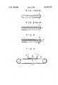
- a conventional data recording mediumwherein a recording layer 2 of a metal such as Te, Bi, Mn or the like is formed on a substrate 1 of glass or a synthetic resin by vacuum deposition, sputtering or the like (FIG. 1).
- a recording layer 2 of a metalsuch as Te, Bi, Mn or the like
- an anticorrosive protective layer 3is formed on the surface of the recording layer 2 (FIG. 2).
- the protective layer 3is generally made of an organic or inorganic material which has resistance to corrosion.
- the protective layer of an inorganic materialis formed on the recording layer into a thin film of less than 5,000 A in thickness, for example, by vacuum deposition, sputtering or the like of silicon dioxide, silicon monoxide, indium oxide or the like.
- the protective layer of an organic materialis formed on the recording layer into a thin film of about 1 to 100 ⁇ , for example, by dissolving in a solvent a polyvinyl chloride resin, styrene resin or the like to provide a solution of the resin and by applying the solution by a suitable means such as a spinner, a roll coater, an applicator or the like.
- the protective layer of an inorganic materialis formed on the recording layer by vacuum deposition or sputtering, cracks tend to form in the recording layer and/or protective layer after a certain period of time.
- the protective layer of an organic materialis formed in place of the protective layer of an inorganic material, the recording layer may flow during application or during curing steps of the protective layer of the organic material. For this reason, the formation of the protective layer of the organic material is cumbersome, and cracks tend to form after a certain period of time.
- a data recording mediumcomprising:
- FIGS. 1 and 2are sectional views of the main part showing an example of a conventional data recording medium
- FIG. 3is a sectional view of the main part showing a data recording medium according to an embodiment of the present invention.
- FIG. 4is a schematic sectional view showing a method for manufacturing a data recording medium according to an embodiment of the present invention.
- FIG. 3is a sectional view of the main part of a data recording medium according to an embodiment of the present invention.
- a data recording mediumhas a substrate 10, a recording layer 11 which is formed on the substrate 10 and on the surface of which is formed an oxide layer 11a, and a protective layer 12 covering the recording layer 11.
- the substrate 10is made of glass or a synthetic resin and is of a disc-shape having a thickness of 0.2 to 2 mm and a diameter of 30 cm.
- the glass or synthetic resin as the material of the substrate 10must transmit light.
- Examples of the synthetic resinmay include a polyolefin such as polyethylene; polyvinyl chloride; a vinyl chloride-acetate copolymer; an ethylene-vinyl acetate copolymer, polycarbonate; polyacrylic acid; polymethacrylic acid; and a lower alkyl ester of polyacrylic acid or polymethacrylic acid.
- a polyolefinsuch as polyethylene; polyvinyl chloride; a vinyl chloride-acetate copolymer; an ethylene-vinyl acetate copolymer, polycarbonate; polyacrylic acid; polymethacrylic acid; and a lower alkyl ester of polyacrylic acid or polymethacrylic acid.
- the recording layer 11is of an annular shape with the central hole (not shown) of the substrate 10 as the center.
- the recording layer 11is a thin film made of a light-reflecting material.
- the light-reflecting materialis required to reflect the laser beam and may be for example Te, Bi, or Al.
- the thickness of the recording layer 11is less than 5,000 A, preferably 200 to 2,000 A.
- the method for forming the recording layer 11 on the surface of the substrate 10may be selected freely only if the recording layer 11 of small thickness can be uniformly formed. The method, therefore, may be a deposition method such as vacuum deposition, sputtering or ion deposition.
- the dense oxide layer 11ais formed on the surface of the recording layer 11 by oxidizing this surface.
- the method for oxidizing the surface of the recording layermay include radiation with ultraviolet rays or infrared rays, heating, standing in the ambient atmosphere, or the like.
- the oxide layer 11ais preferably 20 to 500 A thick.
- radiation with ultraviolet rays or standing in a dry airare preferred since the dense oxide layer is easy to form thereby. If the dense oxide layer is too thin, favorable effects may not be obtained. On the other hand, if the dense oxide layer is too thick, the contrast of the recording bit is difficult to control.
- the protective layer 12is formed so as to cover the oxide layer 11a of the recording layer 11 and to form a concentric ring having the central hole (not shown) of the substrate 10 as a center.
- the protective layer 12may therefore be made of an organic material such as polystyrene, an epoxy resin, a polycarbonate resin, a vinyl chloride-acetate copolymer, an ethylenevinyl acetate copolymer, and a silicone resin.
- the protective layer 12 of an organic material as described abovecan be formed by preparing a solution of the organic material in an organic solvent such as benzene, toluene, or the like, applying the solution on the surface of the oxide layer 11a of the recording layer 11, and removing the organic solvent.
- Said protective layer 12may be formed by using said resin of uncured state without said solvent.
- the protective layer 23may alternatively be made of an inorganic material such as SiO 2 , SiO, In 2 O 3 , SnO 2 , MgO, ZnO, ZnO 2 , Al 2 O 3 , CeO 2 , TiO 2 , MgF 2 , CaF 2 and CeF 3 .
- the protective layer 12 of the inorganic materialis formed on the recording layer by vacuum deposition, sputtering or the like.
- FIG. 4is a schematic view showing an embodiment of the method of manufacturing the data recording medium of the present invention.
- the recording layer 11 of Teis formed to a thickness of 500 A by vacuum deposition on the surface of the substrate 10 of an acrylics.
- the whole structureis fed to a heating section by a supply belt 15 at a rate of 5 m/min.
- the heating sectionhas an arranging distance L (50 cm) in which three focusing type ultraviolet lamps 14 of 80 W/cm are arranged.
- the oxide layer 11aof about 100 A thickness as shown in FIG. 3 is formed on the surface of the recording layer 11.
- a styrene resinis coated on the surface of the recording layer 11 to a thickness of 20 ⁇ m by spinner coating to form the protective layer 12 as shown in FIG. 3.
- the recording layer 11 of Te and of 400 A thicknessis formed on the surface of the substrate 10 of the acrylics.
- the surface layer of the recording layer 11is oxidized to form the oxide layer 11a (TeO x ) of 100 A thickness.
- the protective layer 12 of a styrene resinis formed thereover. Therefore, since the oxide layer 11a is formed on the surface of the recording layer 11, the recording layer 11 will have good mechanical strength. The formation of the microcracks in the recording layer 11 during formation of the protective layer 12 may therefore be prevented.
- an oxide layeris formed on the surface of a recording layer, so that the recording layer has better mechanical strength and formation of cracks in the recording layer during the formation of the protective layer is prevented. Accordingly, the data recording medium provides advantages such as improvements in the manufacturing yield and the reliability.
Landscapes
- Engineering & Computer Science (AREA)
- Manufacturing & Machinery (AREA)
- Optical Record Carriers And Manufacture Thereof (AREA)
- Thermal Transfer Or Thermal Recording In General (AREA)
- Manufacturing Optical Record Carriers (AREA)
Abstract
Description
Claims (5)
Applications Claiming Priority (2)
| Application Number | Priority Date | Filing Date | Title |
|---|---|---|---|
| JP56014979AJPS57130241A (en) | 1981-02-05 | 1981-02-05 | Information storage medium |
| JP56-14979 | 1981-02-05 |
Publications (1)
| Publication Number | Publication Date |
|---|---|
| US4403231Atrue US4403231A (en) | 1983-09-06 |
Family
ID=11876085
Family Applications (1)
| Application Number | Title | Priority Date | Filing Date |
|---|---|---|---|
| US06/343,983Expired - Fee RelatedUS4403231A (en) | 1981-02-05 | 1982-01-29 | Data recording medium |
Country Status (4)
| Country | Link |
|---|---|
| US (1) | US4403231A (en) |
| JP (1) | JPS57130241A (en) |
| DE (1) | DE3202821A1 (en) |
| NL (1) | NL8200393A (en) |
Cited By (13)
| Publication number | Priority date | Publication date | Assignee | Title |
|---|---|---|---|---|
| US4493887A (en)* | 1982-11-05 | 1985-01-15 | U.S. Philips Corporation | Optical recording element |
| EP0141949A1 (en)* | 1983-09-19 | 1985-05-22 | Siemens Aktiengesellschaft | Electrical device with recording facility |
| US4527173A (en)* | 1984-04-16 | 1985-07-02 | Eastman Kodak Company | Erasable, reusable optical recording element and method |
| US4584259A (en)* | 1982-12-17 | 1986-04-22 | Burroughs Corporation | Coated media for optical recording with acrylic overcoat |
| US4587209A (en)* | 1984-03-28 | 1986-05-06 | Matsushita Electric Industrial Co., Ltd. | Optical information recording member comprising Au, TeO2 and Te |
| US4599298A (en)* | 1984-07-16 | 1986-07-08 | Minnesota Mining And Manufacturing Company | Graphic arts imaging constructions using vapor-deposited layers |
| US4625215A (en)* | 1984-07-06 | 1986-11-25 | Storage Technology Corporation | Optical storage structure |
| US4636804A (en)* | 1985-01-11 | 1987-01-13 | Celanese Corporation | Recording medium comprising a microporous polymer exhibiting enhanced signal to noise ratio |
| US4657840A (en)* | 1984-07-16 | 1987-04-14 | Minnesota Mining And Manufacturing Company | Graphic arts imaging constructions using vapor-deposited layers |
| US4786538A (en)* | 1984-12-13 | 1988-11-22 | Kuraray Co., Ltd. | Optical recording medium formed of chalcogenide oxide and method for producing the same |
| US4831608A (en)* | 1984-02-22 | 1989-05-16 | Daicel Chemical Industries, Ltd. | Multi-layer high density information recording carrier having a non-alkali inorganic glass protective layer |
| US4878212A (en)* | 1984-10-05 | 1989-10-31 | Hoechst Celanese Corporation | Optical recording medium comprising a microporous polymer recording layer |
| US4943957A (en)* | 1985-06-18 | 1990-07-24 | Daicel Chemical Industries, Ltd. | High-density information recording carrier |
Families Citing this family (6)
| Publication number | Priority date | Publication date | Assignee | Title |
|---|---|---|---|---|
| JPS58224446A (en)* | 1982-06-23 | 1983-12-26 | Hitachi Ltd | Recording parts |
| US4514439A (en)* | 1983-09-16 | 1985-04-30 | Rohm And Haas Company | Dust cover |
| JPS62121767A (en)* | 1985-11-20 | 1987-06-03 | Olympus Optical Co Ltd | Substrate for information recording medium |
| JP2531626B2 (en)* | 1986-04-10 | 1996-09-04 | オリンパス光学工業株式会社 | Optical characteristic measuring device for optical recording medium substrate |
| JPS62273634A (en)* | 1986-05-21 | 1987-11-27 | Hitachi Ltd | Optical information recording and reproducing |
| US5328813A (en)* | 1992-06-30 | 1994-07-12 | The Dow Chemical Company | Method for the preparation of optical recording media containing overcoat |
Citations (8)
| Publication number | Priority date | Publication date | Assignee | Title |
|---|---|---|---|---|
| US3560994A (en)* | 1968-02-06 | 1971-02-02 | Bosch Gmbh Robert | Vaporizable recording medium |
| US3657721A (en)* | 1969-09-11 | 1972-04-18 | Bosch Gmbh Robert | Recording tape with partially oxidized aluminum film |
| US3665483A (en)* | 1969-06-06 | 1972-05-23 | Chase Manhattan Capital Corp | Laser recording medium |
| DE2522928A1 (en)* | 1974-05-25 | 1975-12-04 | Canon Kk | RECORDING MEDIA AND METHOD |
| US3996057A (en)* | 1972-12-07 | 1976-12-07 | Fuji Photo Film Co., Ltd. | Heat development process for forming images utilizing a photographic material containing a metal layer and an inorganic material layer |
| US4069487A (en)* | 1974-12-26 | 1978-01-17 | Canon Kabushiki Kaisha | Recording member and process for recording |
| NL7804656A (en) | 1977-08-29 | 1979-03-02 | Rca Corp | UNTREATED REGISTRATION CARRIER. |
| US4188214A (en)* | 1975-08-11 | 1980-02-12 | Fuji Photo Film Co., Ltd. | Recording material |
Family Cites Families (1)
| Publication number | Priority date | Publication date | Assignee | Title |
|---|---|---|---|---|
| JPS5557495A (en)* | 1978-10-25 | 1980-04-28 | Fuji Photo Film Co Ltd | Thermal recording medium |
- 1981
- 1981-02-05JPJP56014979Apatent/JPS57130241A/enactivePending
- 1982
- 1982-01-29DEDE19823202821patent/DE3202821A1/ennot_activeCeased
- 1982-01-29USUS06/343,983patent/US4403231A/ennot_activeExpired - Fee Related
- 1982-02-03NLNL8200393Apatent/NL8200393A/ennot_activeApplication Discontinuation
Patent Citations (8)
| Publication number | Priority date | Publication date | Assignee | Title |
|---|---|---|---|---|
| US3560994A (en)* | 1968-02-06 | 1971-02-02 | Bosch Gmbh Robert | Vaporizable recording medium |
| US3665483A (en)* | 1969-06-06 | 1972-05-23 | Chase Manhattan Capital Corp | Laser recording medium |
| US3657721A (en)* | 1969-09-11 | 1972-04-18 | Bosch Gmbh Robert | Recording tape with partially oxidized aluminum film |
| US3996057A (en)* | 1972-12-07 | 1976-12-07 | Fuji Photo Film Co., Ltd. | Heat development process for forming images utilizing a photographic material containing a metal layer and an inorganic material layer |
| DE2522928A1 (en)* | 1974-05-25 | 1975-12-04 | Canon Kk | RECORDING MEDIA AND METHOD |
| US4069487A (en)* | 1974-12-26 | 1978-01-17 | Canon Kabushiki Kaisha | Recording member and process for recording |
| US4188214A (en)* | 1975-08-11 | 1980-02-12 | Fuji Photo Film Co., Ltd. | Recording material |
| NL7804656A (en) | 1977-08-29 | 1979-03-02 | Rca Corp | UNTREATED REGISTRATION CARRIER. |
Cited By (13)
| Publication number | Priority date | Publication date | Assignee | Title |
|---|---|---|---|---|
| US4493887A (en)* | 1982-11-05 | 1985-01-15 | U.S. Philips Corporation | Optical recording element |
| US4584259A (en)* | 1982-12-17 | 1986-04-22 | Burroughs Corporation | Coated media for optical recording with acrylic overcoat |
| EP0141949A1 (en)* | 1983-09-19 | 1985-05-22 | Siemens Aktiengesellschaft | Electrical device with recording facility |
| US4831608A (en)* | 1984-02-22 | 1989-05-16 | Daicel Chemical Industries, Ltd. | Multi-layer high density information recording carrier having a non-alkali inorganic glass protective layer |
| US4587209A (en)* | 1984-03-28 | 1986-05-06 | Matsushita Electric Industrial Co., Ltd. | Optical information recording member comprising Au, TeO2 and Te |
| US4527173A (en)* | 1984-04-16 | 1985-07-02 | Eastman Kodak Company | Erasable, reusable optical recording element and method |
| US4625215A (en)* | 1984-07-06 | 1986-11-25 | Storage Technology Corporation | Optical storage structure |
| US4657840A (en)* | 1984-07-16 | 1987-04-14 | Minnesota Mining And Manufacturing Company | Graphic arts imaging constructions using vapor-deposited layers |
| US4599298A (en)* | 1984-07-16 | 1986-07-08 | Minnesota Mining And Manufacturing Company | Graphic arts imaging constructions using vapor-deposited layers |
| US4878212A (en)* | 1984-10-05 | 1989-10-31 | Hoechst Celanese Corporation | Optical recording medium comprising a microporous polymer recording layer |
| US4786538A (en)* | 1984-12-13 | 1988-11-22 | Kuraray Co., Ltd. | Optical recording medium formed of chalcogenide oxide and method for producing the same |
| US4636804A (en)* | 1985-01-11 | 1987-01-13 | Celanese Corporation | Recording medium comprising a microporous polymer exhibiting enhanced signal to noise ratio |
| US4943957A (en)* | 1985-06-18 | 1990-07-24 | Daicel Chemical Industries, Ltd. | High-density information recording carrier |
Also Published As
| Publication number | Publication date |
|---|---|
| DE3202821A1 (en) | 1982-11-25 |
| NL8200393A (en) | 1982-09-01 |
| JPS57130241A (en) | 1982-08-12 |
Similar Documents
| Publication | Publication Date | Title |
|---|---|---|
| US4403231A (en) | Data recording medium | |
| US4450452A (en) | Data recording medium | |
| EP0375298B1 (en) | Optical information recording media | |
| US4334233A (en) | Optical recording element and its manufacturing method | |
| JPS6042095A (en) | Information recording member and its manufacturing method | |
| HK77786A (en) | Article suitable for information storage | |
| GB2080598A (en) | Optical data storage and recording medium having a replaceable protective coverplate | |
| US4583102A (en) | Optical disc and method of manufacturing | |
| JPS6333210B2 (en) | ||
| JPS6318252B2 (en) | ||
| US4408213A (en) | Reinforced bubble recording medium and information record | |
| CA1214933A (en) | Quadrilayer optical draw medium | |
| US4740447A (en) | Optical recording medium | |
| JPH07105069B2 (en) | Optical recording medium | |
| US4547876A (en) | Optical recording medium and information record and method of making same | |
| EP0188549B1 (en) | Optical storage structure | |
| JPH0442737B2 (en) | ||
| JP7183171B2 (en) | Optical disc and optical disc manufacturing method | |
| JPS57181443A (en) | Information storage medium | |
| JPS6235171B2 (en) | ||
| JPH0754591B2 (en) | Optical recording medium | |
| JPH0561111B2 (en) | ||
| JPH0258740A (en) | Information recording medium and recording method thereof | |
| JPH02302931A (en) | Optical data carrier | |
| JPH0555938B2 (en) |
Legal Events
| Date | Code | Title | Description |
|---|---|---|---|
| AS | Assignment | Owner name:TOKYO SHIBAURA DENKI KABUSHIKI KAISHA, 72 HORIKAWA Free format text:ASSIGNMENT OF ASSIGNORS INTEREST.;ASSIGNORS:ANDO, HIDEO;NAKAGAWA, TOSHIHARU;REEL/FRAME:003974/0306 Effective date:19820118 | |
| MAFP | Maintenance fee payment | Free format text:PAYMENT OF MAINTENANCE FEE, 4TH YEAR, PL 96-517 (ORIGINAL EVENT CODE: M170); ENTITY STATUS OF PATENT OWNER: LARGE ENTITY Year of fee payment:4 | |
| FEPP | Fee payment procedure | Free format text:PAYOR NUMBER ASSIGNED (ORIGINAL EVENT CODE: ASPN); ENTITY STATUS OF PATENT OWNER: LARGE ENTITY | |
| MAFP | Maintenance fee payment | Free format text:PAYMENT OF MAINTENANCE FEE, 8TH YEAR, PL 96-517 (ORIGINAL EVENT CODE: M171); ENTITY STATUS OF PATENT OWNER: LARGE ENTITY Year of fee payment:8 | |
| FEPP | Fee payment procedure | Free format text:MAINTENANCE FEE REMINDER MAILED (ORIGINAL EVENT CODE: REM.); ENTITY STATUS OF PATENT OWNER: LARGE ENTITY | |
| LAPS | Lapse for failure to pay maintenance fees | ||
| FP | Lapsed due to failure to pay maintenance fee | Effective date:19950906 | |
| AS | Assignment | Owner name:VICKERS E.S.D., INC., OHIO Free format text:ASSIGNMENT OF ASSIGNORS INTEREST;ASSIGNOR:CINCINNATI MILACRON INC.;REEL/FRAME:008261/0360 Effective date:19960822 | |
| STCH | Information on status: patent discontinuation | Free format text:PATENT EXPIRED DUE TO NONPAYMENT OF MAINTENANCE FEES UNDER 37 CFR 1.362 |