US4400740A - Intensity control for raster output scanners - Google Patents
Intensity control for raster output scannersDownload PDFInfo
- Publication number
- US4400740A US4400740AUS06/295,438US29543881AUS4400740AUS 4400740 AUS4400740 AUS 4400740AUS 29543881 AUS29543881 AUS 29543881AUS 4400740 AUS4400740 AUS 4400740A
- Authority
- US
- United States
- Prior art keywords
- signals
- intensity
- video image
- signal
- control
- Prior art date
- Legal status (The legal status is an assumption and is not a legal conclusion. Google has not performed a legal analysis and makes no representation as to the accuracy of the status listed.)
- Expired - Lifetime
Links
- 239000002131composite materialSubstances0.000claimsabstractdescription7
- 230000004044responseEffects0.000claimsabstractdescription6
- 108091008695photoreceptorsProteins0.000claimsdescription11
- 238000012937correctionMethods0.000claimsdescription8
- 238000000034methodMethods0.000claimsdescription5
- 230000005670electromagnetic radiationEffects0.000claimsdescription3
- 238000003384imaging methodMethods0.000claims2
- 238000012544monitoring processMethods0.000claims1
- 230000003287optical effectEffects0.000description4
- 230000003068static effectEffects0.000description3
- 230000015556catabolic processEffects0.000description2
- 230000001276controlling effectEffects0.000description2
- 239000013078crystalSubstances0.000description2
- 238000006731degradation reactionMethods0.000description2
- 230000005540biological transmissionEffects0.000description1
- 238000004891communicationMethods0.000description1
- 238000010276constructionMethods0.000description1
- 230000008878couplingEffects0.000description1
- 238000010168coupling processMethods0.000description1
- 238000005859coupling reactionMethods0.000description1
- 238000013461designMethods0.000description1
- 238000010586diagramMethods0.000description1
- 230000009977dual effectEffects0.000description1
- 230000000694effectsEffects0.000description1
- 238000005516engineering processMethods0.000description1
- 230000005284excitationEffects0.000description1
- 238000005286illuminationMethods0.000description1
- 238000005259measurementMethods0.000description1
- 238000012986modificationMethods0.000description1
- 230000004048modificationEffects0.000description1
- 230000003094perturbing effectEffects0.000description1
- 238000002310reflectometryMethods0.000description1
- 230000001105regulatory effectEffects0.000description1
Images
Classifications
- H—ELECTRICITY
- H04—ELECTRIC COMMUNICATION TECHNIQUE
- H04N—PICTORIAL COMMUNICATION, e.g. TELEVISION
- H04N1/00—Scanning, transmission or reproduction of documents or the like, e.g. facsimile transmission; Details thereof
- H04N1/40—Picture signal circuits
- H04N1/40025—Circuits exciting or modulating particular heads for reproducing continuous tone value scales
- H04N1/4005—Circuits exciting or modulating particular heads for reproducing continuous tone value scales with regulating circuits, e.g. dependent upon ambient temperature or feedback control
- H—ELECTRICITY
- H04—ELECTRIC COMMUNICATION TECHNIQUE
- H04N—PICTORIAL COMMUNICATION, e.g. TELEVISION
- H04N1/00—Scanning, transmission or reproduction of documents or the like, e.g. facsimile transmission; Details thereof
- H04N1/40—Picture signal circuits
- H04N1/40025—Circuits exciting or modulating particular heads for reproducing continuous tone value scales
- H04N1/40037—Circuits exciting or modulating particular heads for reproducing continuous tone value scales the reproducing element being a laser
Definitions
- This inventionrelates to raster scanners and more particularly to a control for regulating both the video and intensity of the scanning beam.
- Raster output scannersoften suffer from inherent writing beam intensity variations which may degrade performance in recording data. This is typically represented by a decrease in raster spot intensity at both ends of scan in conventional overfilled and facet tracking polygon illumination systems. Additionally however, intensity non-uniformities caused by other scanner related components can occur from raster line to raster line or over groups of raster lines, for example, non-uniformities in polygon facet reflectivity, laser power degradation, dirt collection on optical surfaces, loss of modulator efficiency, and the like. In previous applications of laser raster scanning, static adjustment of writing beam intensity was applied to compensate for laser power degradation due to the above. Such static adjustment was implemented by incorporating the laser into a feedback loop and electronically controlling laser excitation current.
- Stability criteriawere met by including in the feedback loop a photosensor which monitored laser power and issued error information to a variable laser power supply.
- the laser output powerwas then adjustable, stable, and quiet over the frequency range of D.C. to several kilohertz (kHz).
- the foregoing technique of correcting laser beam intensityrequires that the r.f. driver for the acousto-optic modulator be specially modified and does not accommodate or permit use of un-modified single port type r.f. drivers found with acousto optic modulators.
- the present inventionis intended to overcome this difficulty by enabling both laser beam intensity and video image signal control, but with conventional single port r.f. drivers.
- This inventionrelates to a raster output scanner, comprising in combination, a high intensity beam of electromagnetic radiation; means to scan the beam across a photoreceptor to expose the photoreceptor and create latent electrostatic images thereon in response to image signals; modulator means to modulate the beam in response to control signals, the modulator means having a single port for receiving the control signals; a source of video image signals; a source of beam intensity signals; and means to combine the video image signals with the beam intensity signals to provide the control signals for input to the modulator means port whereby the modulator means modulates both on and off of the beam and beam intensity in accordance with both the video image signals and beam intensity signals.
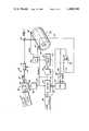
- FIG. 1is a schematic view of an exemplary raster output scanner incorporating the control of the present invention for modulating both the scanning beam on/off and beam intensity through a single port modulator;
- FIG. 2is a view showing details of the single port r.f. driver for the modulator shown in FIG. 1;
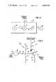
- FIG. 3is a circuit diagram showing details of the control circuit portion of the control shown in FIG. 1.
- Scanner 10includes a suitable source of high intensity light such as a laser 12.
- Power supply 14provides operating power to laser 12.
- the beam 13 of light output by laser 12is passed to an acousto optic modulator 15 which modulates both the video, i.e. the on/off, and intensity of beam 13 as will appear.
- From modulator 15the now modulated beam 13' is passed to a scanning element, herein illustrated in the form of a rotating polygon 17.
- Polygon 17sweeps the modulated beam impinging on the facets 18 thereof across the photosensitive surface 21 of a moving recording member, shown here in the form of a xerographic drum 20 of a conventional xerographic system (not shown).
- Suitable optical elementssuch as mirror 22 may be interposed in the beam optical path to guide and/or focus the beam onto the surface 21 of the drum 20 and provide the requisite beam dimension.
- the term "light”refers to an electromagnetic radiation in the visible, ultraviolet, and infrared portions of the electromagnetic system.
- Acousto optic modulator 15which is of conventional design and construction, comprises an electrically driven piezo electric transducer 25 acoustically coupled to an acousto-optical crystal 26.
- Transducer 25generates an acoustic wave in response to an electrical signal which travels through the crystal 26 perturbing the index of refraction and acting as a phase grating, the grating period being equal to the drive or acoustic frequency with grating density being proportional to the amplitude of the drive signal applied thereto.
- transducer 25without a signal applied to transducer 25, only the non-defracted beam 13" exists.
- Application of a predetermined signal level to transducer 25defracts the beam 13 at an angle ⁇ to produce a defracted light beam 13'.
- modulator 15acts to modulate the intensity of the defracted light beam 13' as will appear.
- driver 30includes a fixed frequency signal source, shown herein as oscillator 32.
- Oscillator 32outputs a signal of constant amplitude and constant frequency through line 31 to a linear balanced mixer 35.
- the r.f. signalis mixed with a composite video image and beam intensity control signal input to linear balanced mixer 35 through line 33.
- the output signal of mixer 35 to line 34is amplified by amplifier 37 and output through line 38 to transducer 25 of modulator 15.
- linear balanced mixer 35is an analog device which enables continuous control over the r.f. signal output of oscillator 32 to the modulator 15 to be continuously controlled. By controlling the r.f.
- control over the r.f. driveris accomplished by combining the digital video image signal with an analog beam intensity control signal to provide a composite control signal which effects not only on/off switching of the writing beam 13' but also control of the beam intensity.
- the composite control signal output in line 33 to r.f. driver 30is derived by control circuit 40.
- Circuit 40includes an input gate 42 to which the digital video image signals are input through lead 43.
- Image signal source 45may for example comprise a memory, communication channel, raster input scanner, and the like.
- the output side of gate 42is coupled through line 44 and resistors 46, 48 to the base of control transistor 50.
- Line 51couples the collector of transistor 50 to a suitable positive reference voltage V.
- Output line 33is connected to the emitter of transistor 50.
- Line 33is tapped by line 53, line 53 being coupled through resistor 54 to a suitable negative reference voltage V.
- Positive and negative reference voltages Vare coupled through lines 60, 61 and resistors 62, 63 respectively to line 44, lines 60, 61 being tapped into line 44 at a point between resistors 46 and 48.
- a beam intensity control signalwhich as will appear may be derived from memory, is input through line 65, line 65 being coupled through resistor 66 and diode 68 to line 44 between resistor 48 and transistor 50.
- positive and negative reference potentials +V, -V respectivelyare + and -5 volts D.C.
- Other component parts of circuit 40are identified as follows:
- the video image signals input to circuit 40 in line 43serve to switch transistor 50 between two operating points within the transistor's linear region.
- the lower pointwhich is set by the bias conditions of transistor 50, fixes the beam off intensity level for beam 13.
- the upper pointwhich is determined by the magnitude of the beam intensity control signal in line 65, fixes the beam on intensity.
- diode 68enters a forward conduction mode to shunt the excess base voltage of transistor 50 to an ideal voltage source, represented by the beam intensity control signal in line 65.
- the beam intensity control signalaccordingly limits the maximum base drive level of transistor 50 to set the maximum transistor emitter voltage thereby providing a composite control signal to r.f. driver 30.
- the beam intensity control signalmay be derived from any suitable circuit or digital technique.
- the beam intensity control signalis derived from beam intensity data stored in a suitable memory such as ROM 80.
- Intensity data stored in ROM 80is suitably obtained, as for example, by running a calibration sequence on scanner 10 before use. Calibration may be carried out by scanning beam 13' across the surface 21 of drum 20 while measuring beam intensity at various selected points along the beam scan line.
- the beam intensity measurementswhich are normally analog signals, are converted to digital signals by a suitable analog-to-digital converter (not shown) and stored in ROM 80 pending use.
- the intensity of the beam 13is normally at a maximum adjacent the center of the scan line with intensity fall-off at both ends of the scan line.
- a suitable pixel clock 82is provided for generating pixel clock signals for clocking the video image signals, clock signals from clock 82 being input to image data source 45 through clock lead 87.
- suitable start of scan (SOS) and end of scan (EOS) detectors 94, 95are provided in the path of scanning beam 13' to detect when beam 13' enters and leaves the operating margins of the photosensitive surface 21.
- the signal outputs of SOS and EOS detectors 94, 95respectively are fed to a suitable video control flip flop 96.
- the output of flip flop 96 to line 97controls enablement of image data source 45 such that video image signals are output to circuit 40 during the period when scanning beam 13' is within the operating margins of photosensitive surface 21.
- An address counter 83is provided to progressively address ROM 80, bus 85 coupling counter to ROM 80.
- Pixel clock 82which is coupled to address counter 83 by clock line 84, serves to clock counter 83 in synchronism with the clocking of video image signals from image data source 45.
- the signal output of control flip flop 96serves to control enabling of address counter 83 to correlate output of beam intensity data stored in ROM 80 with input of video image signals from image data source 45 on a line by line basis.
- the output of ROM 80is coupled by bus 86 to a D/A converter 88 which converts the digital signal output of ROM 80 to an analog signal.
- the signal output by D/A converter 88is fed to op amp 92 through line 88'.
- the output of op amp 92which may comprise a Texas Instruments Model T.I. 747 op amp, is coupled by line 65 to control circuit 40.
- a suitable light intensity detector 89is disposed in the path of beam 13 to measure beam intensity.
- the signal output by detector 89is fed through line 90 to op amp 92 where the signal is used to update the corrective signal output by ROM 80.
- the output of op amp 92comprises the beam intensity control signal input to control circuit 40.
Landscapes
- Engineering & Computer Science (AREA)
- Multimedia (AREA)
- Signal Processing (AREA)
- Physics & Mathematics (AREA)
- Optics & Photonics (AREA)
- Facsimile Scanning Arrangements (AREA)
Abstract
Description
______________________________________Resistor 46 39ohms Resistor 48 47ohms Resistor 62 160ohms Resistor 63 390 ohms Resistor 66 10ohms Resistor 54 220 ohms Gate 42 Texas Instrument (T.I.) 74S20Transistor 50 Texas Instrument (T.I.)2N3866 Diode 68 Motorola MBD 101 ______________________________________
Claims (6)
Priority Applications (1)
| Application Number | Priority Date | Filing Date | Title |
|---|---|---|---|
| US06/295,438US4400740A (en) | 1981-08-24 | 1981-08-24 | Intensity control for raster output scanners |
Applications Claiming Priority (1)
| Application Number | Priority Date | Filing Date | Title |
|---|---|---|---|
| US06/295,438US4400740A (en) | 1981-08-24 | 1981-08-24 | Intensity control for raster output scanners |
Publications (1)
| Publication Number | Publication Date |
|---|---|
| US4400740Atrue US4400740A (en) | 1983-08-23 |
Family
ID=23137737
Family Applications (1)
| Application Number | Title | Priority Date | Filing Date |
|---|---|---|---|
| US06/295,438Expired - LifetimeUS4400740A (en) | 1981-08-24 | 1981-08-24 | Intensity control for raster output scanners |
Country Status (1)
| Country | Link |
|---|---|
| US (1) | US4400740A (en) |
Cited By (73)
| Publication number | Priority date | Publication date | Assignee | Title |
|---|---|---|---|---|
| FR2539525A1 (en)* | 1983-01-18 | 1984-07-20 | Dainippon Screen Mfg | METHOD FOR CORRECTING THE INTENSITY OF A BEAM DURING THE ANALYSIS AND RECORDING OF A FIGURE |
| US4577933A (en)* | 1983-12-15 | 1986-03-25 | Xerox Corporation | Gap modulator for high speed scanners |
| EP0179554A1 (en)* | 1984-08-27 | 1986-04-30 | Minnesota Mining And Manufacturing Company | Continuous tone recording system |
| US4587531A (en)* | 1984-11-05 | 1986-05-06 | Eastman Kodak Company | Clock signal producing apparatus |
| US4620236A (en)* | 1984-11-09 | 1986-10-28 | Sharp Kabushiki Kaisha | Image picture reading device |
| US4686363A (en)* | 1986-01-21 | 1987-08-11 | Printware, Inc. | Self-resonant scanner biasing system |
| US4692016A (en)* | 1986-03-14 | 1987-09-08 | Fondation Suisse Pour La Recherche En Microtechnique | Process for electrophotographic matrix printing and device for carrying out the process |
| EP0158669B1 (en)* | 1983-10-03 | 1987-12-02 | EASTMAN KODAK COMPANY (a New Jersey corporation) | Method and apparatus for controlling charge on a photoconductor |
| US4733064A (en)* | 1985-02-13 | 1988-03-22 | Fuji Photo Film Co., Ltd. | Light beam scanner with focus-varying mechanism |
| US4748465A (en)* | 1983-10-03 | 1988-05-31 | Eastman Kodak Company | Method and apparatus for controlling charge on a photoconductor |
| US4800442A (en)* | 1985-08-15 | 1989-01-24 | Canon Kabushiki Kaisha | Apparatus for generating an image from a digital video signal |
| FR2632245A1 (en)* | 1988-06-01 | 1989-12-08 | Selisa | Method of printing with grey levels and graphics printer |
| US4888647A (en)* | 1987-12-21 | 1989-12-19 | Minolta Camera Kabushiki Kaisha | Image recording apparatus with improved SOS detection |
| US4920430A (en)* | 1986-10-29 | 1990-04-24 | Dainippon Screen Mfg. Co., Ltd. | Method of and apparatus for jitter correction of a polygon mirror in an image recording apparatus |
| US5055860A (en)* | 1989-05-19 | 1991-10-08 | Ricoh Company, Ltd. | Image forming apparatus |
| US5083141A (en)* | 1989-08-30 | 1992-01-21 | Ricoh Company, Ltd. | Image forming apparatus |
| US5151586A (en)* | 1990-08-01 | 1992-09-29 | Brother Kogyo Kabushiki Kaisha | Scanning exposure device provided with intensity correction to compensate for scan angle |
| US5164843A (en)* | 1990-06-18 | 1992-11-17 | Olive Tree Technology, Inc. | Scanner with a linearized vco pixel clock |
| US5165074A (en)* | 1990-08-20 | 1992-11-17 | Xerox Corporation | Means and method for controlling raster output scanner intensity |
| US5166944A (en)* | 1991-06-07 | 1992-11-24 | Advanced Laser Technologies, Inc. | Laser beam scanning apparatus and method |
| JPH06175055A (en)* | 1992-07-31 | 1994-06-24 | E I Du Pont De Nemours & Co | Scanning system and error correction for scanning system |
| WO1994017624A1 (en)* | 1993-01-29 | 1994-08-04 | Minnesota Mining And Manufacturing Company | Method and apparatus for reducing the effects of laser noise and for improving modulation transfer function in scanning a photoconductive surface |
| EP0695078A1 (en) | 1994-07-29 | 1996-01-31 | Xerox Corporation | Fast scan spot correction in a polygon raster output scanner |
| US5687020A (en)* | 1995-06-29 | 1997-11-11 | Samsung Electronics Co., Ltd. | Image projector using acousto-optic tunable filter |
| US20010022382A1 (en)* | 1998-07-29 | 2001-09-20 | Shook James Gill | Method of and apparatus for sealing an hermetic lid to a semiconductor die |
| US20020098610A1 (en)* | 2001-01-19 | 2002-07-25 | Alexander Payne | Reduced surface charging in silicon-based devices |
| US20020186448A1 (en)* | 2001-04-10 | 2002-12-12 | Silicon Light Machines | Angled illumination for a single order GLV based projection system |
| US20020196226A1 (en)* | 1999-08-05 | 2002-12-26 | Microvision, Inc. | Scanned display with variation compensation |
| US20020196492A1 (en)* | 2001-06-25 | 2002-12-26 | Silicon Light Machines | Method and apparatus for dynamic equalization in wavelength division multiplexing |
| US20030025984A1 (en)* | 2001-08-01 | 2003-02-06 | Chris Gudeman | Optical mem device with encapsulated dampening gas |
| US20030035189A1 (en)* | 2001-08-15 | 2003-02-20 | Amm David T. | Stress tuned blazed grating light valve |
| US20030103194A1 (en)* | 2001-11-30 | 2003-06-05 | Gross Kenneth P. | Display apparatus including RGB color combiner and 1D light valve relay including schlieren filter |
| US20040001257A1 (en)* | 2001-03-08 | 2004-01-01 | Akira Tomita | High contrast grating light valve |
| US20040008399A1 (en)* | 2001-06-25 | 2004-01-15 | Trisnadi Jahja I. | Method, apparatus, and diffuser for reducing laser speckle |
| US6712480B1 (en) | 2002-09-27 | 2004-03-30 | Silicon Light Machines | Controlled curvature of stressed micro-structures |
| US6714337B1 (en) | 2002-06-28 | 2004-03-30 | Silicon Light Machines | Method and device for modulating a light beam and having an improved gamma response |
| US6728023B1 (en) | 2002-05-28 | 2004-04-27 | Silicon Light Machines | Optical device arrays with optimized image resolution |
| US6767751B2 (en) | 2002-05-28 | 2004-07-27 | Silicon Light Machines, Inc. | Integrated driver process flow |
| US6800238B1 (en) | 2002-01-15 | 2004-10-05 | Silicon Light Machines, Inc. | Method for domain patterning in low coercive field ferroelectrics |
| US6801354B1 (en) | 2002-08-20 | 2004-10-05 | Silicon Light Machines, Inc. | 2-D diffraction grating for substantially eliminating polarization dependent losses |
| US6806997B1 (en) | 2003-02-28 | 2004-10-19 | Silicon Light Machines, Inc. | Patterned diffractive light modulator ribbon for PDL reduction |
| US6813059B2 (en) | 2002-06-28 | 2004-11-02 | Silicon Light Machines, Inc. | Reduced formation of asperities in contact micro-structures |
| US6822797B1 (en) | 2002-05-31 | 2004-11-23 | Silicon Light Machines, Inc. | Light modulator structure for producing high-contrast operation using zero-order light |
| US6829258B1 (en) | 2002-06-26 | 2004-12-07 | Silicon Light Machines, Inc. | Rapidly tunable external cavity laser |
| US6829092B2 (en) | 2001-08-15 | 2004-12-07 | Silicon Light Machines, Inc. | Blazed grating light valve |
| US6865346B1 (en)* | 2001-06-05 | 2005-03-08 | Silicon Light Machines Corporation | Fiber optic transceiver |
| US6872984B1 (en) | 1998-07-29 | 2005-03-29 | Silicon Light Machines Corporation | Method of sealing a hermetic lid to a semiconductor die at an angle |
| US6908201B2 (en) | 2002-06-28 | 2005-06-21 | Silicon Light Machines Corporation | Micro-support structures |
| US6922273B1 (en) | 2003-02-28 | 2005-07-26 | Silicon Light Machines Corporation | PDL mitigation structure for diffractive MEMS and gratings |
| US6922272B1 (en) | 2003-02-14 | 2005-07-26 | Silicon Light Machines Corporation | Method and apparatus for leveling thermal stress variations in multi-layer MEMS devices |
| US6927891B1 (en) | 2002-12-23 | 2005-08-09 | Silicon Light Machines Corporation | Tilt-able grating plane for improved crosstalk in 1×N blaze switches |
| US6928207B1 (en) | 2002-12-12 | 2005-08-09 | Silicon Light Machines Corporation | Apparatus for selectively blocking WDM channels |
| US6934070B1 (en) | 2002-12-18 | 2005-08-23 | Silicon Light Machines Corporation | Chirped optical MEM device |
| US6947613B1 (en) | 2003-02-11 | 2005-09-20 | Silicon Light Machines Corporation | Wavelength selective switch and equalizer |
| US6956995B1 (en) | 2001-11-09 | 2005-10-18 | Silicon Light Machines Corporation | Optical communication arrangement |
| US6956878B1 (en) | 2000-02-07 | 2005-10-18 | Silicon Light Machines Corporation | Method and apparatus for reducing laser speckle using polarization averaging |
| US6987600B1 (en) | 2002-12-17 | 2006-01-17 | Silicon Light Machines Corporation | Arbitrary phase profile for better equalization in dynamic gain equalizer |
| US6991953B1 (en) | 2001-09-13 | 2006-01-31 | Silicon Light Machines Corporation | Microelectronic mechanical system and methods |
| US7027202B1 (en) | 2003-02-28 | 2006-04-11 | Silicon Light Machines Corp | Silicon substrate as a light modulator sacrificial layer |
| US7042611B1 (en) | 2003-03-03 | 2006-05-09 | Silicon Light Machines Corporation | Pre-deflected bias ribbons |
| US7054515B1 (en) | 2002-05-30 | 2006-05-30 | Silicon Light Machines Corporation | Diffractive light modulator-based dynamic equalizer with integrated spectral monitor |
| US7057819B1 (en) | 2002-12-17 | 2006-06-06 | Silicon Light Machines Corporation | High contrast tilting ribbon blazed grating |
| US7057795B2 (en) | 2002-08-20 | 2006-06-06 | Silicon Light Machines Corporation | Micro-structures with individually addressable ribbon pairs |
| US7068372B1 (en) | 2003-01-28 | 2006-06-27 | Silicon Light Machines Corporation | MEMS interferometer-based reconfigurable optical add-and-drop multiplexor |
| US20070008594A1 (en)* | 2005-07-06 | 2007-01-11 | Xerox Corporation | Method and system for improving print quality |
| US7286764B1 (en) | 2003-02-03 | 2007-10-23 | Silicon Light Machines Corporation | Reconfigurable modulator-based optical add-and-drop multiplexer |
| US20080062161A1 (en)* | 1999-08-05 | 2008-03-13 | Microvision, Inc. | Apparatuses and methods for utilizing non-ideal light sources |
| US7391973B1 (en) | 2003-02-28 | 2008-06-24 | Silicon Light Machines Corporation | Two-stage gain equalizer |
| US20110052228A1 (en)* | 2009-08-27 | 2011-03-03 | Xerox Corporation | Method and system for banding compensation using electrostatic voltmeter based sensing |
| US20110058186A1 (en)* | 2009-09-08 | 2011-03-10 | Xerox Corporation | Least squares based coherent multipage analysis of printer banding for diagnostics and compensation |
| US20110058184A1 (en)* | 2009-09-08 | 2011-03-10 | Xerox Corporation | Least squares based exposure modulation for banding compensation |
| US20110058226A1 (en)* | 2009-09-08 | 2011-03-10 | Xerox Corporation | Banding profile estimation using spline interpolation |
| US9699352B1 (en)* | 2015-12-30 | 2017-07-04 | Lexmark International, Inc. | Laser scanning unit adjusting output power of modulated beam using shading information to reduce scan line energy variation |
Citations (12)
| Publication number | Priority date | Publication date | Assignee | Title |
|---|---|---|---|---|
| US3524147A (en)* | 1967-03-29 | 1970-08-11 | Union Carbide Corp | Method and apparatus for the electro-optic control and modulation of light |
| US3806834A (en)* | 1972-07-06 | 1974-04-23 | Cal Inst Of Technology | Stark-effect modulation of co{11 {11 laser with nh{11 d |
| US3875400A (en)* | 1971-04-06 | 1975-04-01 | Pao Yoh Han | Intensity modulated optical carrier communication system |
| US3895317A (en)* | 1971-04-29 | 1975-07-15 | Rca Corp | Control circuits |
| US4009385A (en)* | 1976-03-22 | 1977-02-22 | Bell Telephone Laboratories, Incorporated | Laser control circuit |
| US4070696A (en)* | 1976-05-10 | 1978-01-24 | Teletype Corporation | Method and apparatus for cancelling nontonal variations in a facsimile scanner output signal |
| US4087838A (en)* | 1975-07-25 | 1978-05-02 | Canon Kabushiki Kaisha | Apparatus for obtaining a light carrying information therewith |
| US4122462A (en)* | 1974-09-11 | 1978-10-24 | Canon Kabushiki Kaisha | Image information recording apparatus |
| US4149071A (en)* | 1976-05-25 | 1979-04-10 | Fujitsu Limited | Light emitting element drive system |
| US4205348A (en)* | 1978-07-05 | 1980-05-27 | Xerox Corporation | Laser scanning utilizing facet tracking and acousto pulse imaging techniques |
| US4270131A (en)* | 1979-11-23 | 1981-05-26 | Tompkins E Neal | Adaptive error correction device for a laser scanner |
| US4336981A (en)* | 1977-10-25 | 1982-06-29 | Ricoh Co., Ltd. | Simultaneous multi-beam optical modulation system |
- 1981
- 1981-08-24USUS06/295,438patent/US4400740A/ennot_activeExpired - Lifetime
Patent Citations (12)
| Publication number | Priority date | Publication date | Assignee | Title |
|---|---|---|---|---|
| US3524147A (en)* | 1967-03-29 | 1970-08-11 | Union Carbide Corp | Method and apparatus for the electro-optic control and modulation of light |
| US3875400A (en)* | 1971-04-06 | 1975-04-01 | Pao Yoh Han | Intensity modulated optical carrier communication system |
| US3895317A (en)* | 1971-04-29 | 1975-07-15 | Rca Corp | Control circuits |
| US3806834A (en)* | 1972-07-06 | 1974-04-23 | Cal Inst Of Technology | Stark-effect modulation of co{11 {11 laser with nh{11 d |
| US4122462A (en)* | 1974-09-11 | 1978-10-24 | Canon Kabushiki Kaisha | Image information recording apparatus |
| US4087838A (en)* | 1975-07-25 | 1978-05-02 | Canon Kabushiki Kaisha | Apparatus for obtaining a light carrying information therewith |
| US4009385A (en)* | 1976-03-22 | 1977-02-22 | Bell Telephone Laboratories, Incorporated | Laser control circuit |
| US4070696A (en)* | 1976-05-10 | 1978-01-24 | Teletype Corporation | Method and apparatus for cancelling nontonal variations in a facsimile scanner output signal |
| US4149071A (en)* | 1976-05-25 | 1979-04-10 | Fujitsu Limited | Light emitting element drive system |
| US4336981A (en)* | 1977-10-25 | 1982-06-29 | Ricoh Co., Ltd. | Simultaneous multi-beam optical modulation system |
| US4205348A (en)* | 1978-07-05 | 1980-05-27 | Xerox Corporation | Laser scanning utilizing facet tracking and acousto pulse imaging techniques |
| US4270131A (en)* | 1979-11-23 | 1981-05-26 | Tompkins E Neal | Adaptive error correction device for a laser scanner |
Cited By (91)
| Publication number | Priority date | Publication date | Assignee | Title |
|---|---|---|---|---|
| FR2539525A1 (en)* | 1983-01-18 | 1984-07-20 | Dainippon Screen Mfg | METHOD FOR CORRECTING THE INTENSITY OF A BEAM DURING THE ANALYSIS AND RECORDING OF A FIGURE |
| EP0158669B1 (en)* | 1983-10-03 | 1987-12-02 | EASTMAN KODAK COMPANY (a New Jersey corporation) | Method and apparatus for controlling charge on a photoconductor |
| US4748465A (en)* | 1983-10-03 | 1988-05-31 | Eastman Kodak Company | Method and apparatus for controlling charge on a photoconductor |
| US4577933A (en)* | 1983-12-15 | 1986-03-25 | Xerox Corporation | Gap modulator for high speed scanners |
| EP0179554A1 (en)* | 1984-08-27 | 1986-04-30 | Minnesota Mining And Manufacturing Company | Continuous tone recording system |
| US4587531A (en)* | 1984-11-05 | 1986-05-06 | Eastman Kodak Company | Clock signal producing apparatus |
| US4620236A (en)* | 1984-11-09 | 1986-10-28 | Sharp Kabushiki Kaisha | Image picture reading device |
| US4733064A (en)* | 1985-02-13 | 1988-03-22 | Fuji Photo Film Co., Ltd. | Light beam scanner with focus-varying mechanism |
| USRE38942E1 (en)* | 1985-08-15 | 2006-01-24 | Canon Inc. | Apparatus for generating an image from a digital video signal |
| US4800442A (en)* | 1985-08-15 | 1989-01-24 | Canon Kabushiki Kaisha | Apparatus for generating an image from a digital video signal |
| US4686363A (en)* | 1986-01-21 | 1987-08-11 | Printware, Inc. | Self-resonant scanner biasing system |
| US4692016A (en)* | 1986-03-14 | 1987-09-08 | Fondation Suisse Pour La Recherche En Microtechnique | Process for electrophotographic matrix printing and device for carrying out the process |
| US4920430A (en)* | 1986-10-29 | 1990-04-24 | Dainippon Screen Mfg. Co., Ltd. | Method of and apparatus for jitter correction of a polygon mirror in an image recording apparatus |
| US4888647A (en)* | 1987-12-21 | 1989-12-19 | Minolta Camera Kabushiki Kaisha | Image recording apparatus with improved SOS detection |
| FR2632245A1 (en)* | 1988-06-01 | 1989-12-08 | Selisa | Method of printing with grey levels and graphics printer |
| US5055860A (en)* | 1989-05-19 | 1991-10-08 | Ricoh Company, Ltd. | Image forming apparatus |
| US5083141A (en)* | 1989-08-30 | 1992-01-21 | Ricoh Company, Ltd. | Image forming apparatus |
| US5164843A (en)* | 1990-06-18 | 1992-11-17 | Olive Tree Technology, Inc. | Scanner with a linearized vco pixel clock |
| US5151586A (en)* | 1990-08-01 | 1992-09-29 | Brother Kogyo Kabushiki Kaisha | Scanning exposure device provided with intensity correction to compensate for scan angle |
| US5165074A (en)* | 1990-08-20 | 1992-11-17 | Xerox Corporation | Means and method for controlling raster output scanner intensity |
| US5646766A (en)* | 1991-06-07 | 1997-07-08 | Advanced Laser Technologies, Inc. | Laser beam scanning apparatus and method |
| US5166944A (en)* | 1991-06-07 | 1992-11-24 | Advanced Laser Technologies, Inc. | Laser beam scanning apparatus and method |
| JP2834978B2 (en) | 1992-07-31 | 1998-12-14 | イー・アイ・デュポン・ドゥ・ヌムール・アンド・カンパニー | Scanning system |
| US5453851A (en)* | 1992-07-31 | 1995-09-26 | E. I. Du Pont De Nemours And Company | Error reduction methods in scanning systems |
| JPH06175055A (en)* | 1992-07-31 | 1994-06-24 | E I Du Pont De Nemours & Co | Scanning system and error correction for scanning system |
| US5340975A (en)* | 1993-01-29 | 1994-08-23 | Minnesota Mining And Manufacturing Company | Method and apparatus for reducing the effects of laser noise and for improving modulation transfer function in scanning a photoconductive surface |
| WO1994017624A1 (en)* | 1993-01-29 | 1994-08-04 | Minnesota Mining And Manufacturing Company | Method and apparatus for reducing the effects of laser noise and for improving modulation transfer function in scanning a photoconductive surface |
| EP0695078A1 (en) | 1994-07-29 | 1996-01-31 | Xerox Corporation | Fast scan spot correction in a polygon raster output scanner |
| US5687020A (en)* | 1995-06-29 | 1997-11-11 | Samsung Electronics Co., Ltd. | Image projector using acousto-optic tunable filter |
| US20010022382A1 (en)* | 1998-07-29 | 2001-09-20 | Shook James Gill | Method of and apparatus for sealing an hermetic lid to a semiconductor die |
| US6872984B1 (en) | 1998-07-29 | 2005-03-29 | Silicon Light Machines Corporation | Method of sealing a hermetic lid to a semiconductor die at an angle |
| US6764875B2 (en) | 1998-07-29 | 2004-07-20 | Silicon Light Machines | Method of and apparatus for sealing an hermetic lid to a semiconductor die |
| US20080062161A1 (en)* | 1999-08-05 | 2008-03-13 | Microvision, Inc. | Apparatuses and methods for utilizing non-ideal light sources |
| US20020196226A1 (en)* | 1999-08-05 | 2002-12-26 | Microvision, Inc. | Scanned display with variation compensation |
| US6661393B2 (en)* | 1999-08-05 | 2003-12-09 | Microvision, Inc. | Scanned display with variation compensation |
| US6956878B1 (en) | 2000-02-07 | 2005-10-18 | Silicon Light Machines Corporation | Method and apparatus for reducing laser speckle using polarization averaging |
| US20020098610A1 (en)* | 2001-01-19 | 2002-07-25 | Alexander Payne | Reduced surface charging in silicon-based devices |
| US20040001257A1 (en)* | 2001-03-08 | 2004-01-01 | Akira Tomita | High contrast grating light valve |
| US7177081B2 (en) | 2001-03-08 | 2007-02-13 | Silicon Light Machines Corporation | High contrast grating light valve type device |
| US6707591B2 (en) | 2001-04-10 | 2004-03-16 | Silicon Light Machines | Angled illumination for a single order light modulator based projection system |
| US20020186448A1 (en)* | 2001-04-10 | 2002-12-12 | Silicon Light Machines | Angled illumination for a single order GLV based projection system |
| US6865346B1 (en)* | 2001-06-05 | 2005-03-08 | Silicon Light Machines Corporation | Fiber optic transceiver |
| US20020196492A1 (en)* | 2001-06-25 | 2002-12-26 | Silicon Light Machines | Method and apparatus for dynamic equalization in wavelength division multiplexing |
| US6747781B2 (en) | 2001-06-25 | 2004-06-08 | Silicon Light Machines, Inc. | Method, apparatus, and diffuser for reducing laser speckle |
| US6782205B2 (en) | 2001-06-25 | 2004-08-24 | Silicon Light Machines | Method and apparatus for dynamic equalization in wavelength division multiplexing |
| US20040008399A1 (en)* | 2001-06-25 | 2004-01-15 | Trisnadi Jahja I. | Method, apparatus, and diffuser for reducing laser speckle |
| US20030025984A1 (en)* | 2001-08-01 | 2003-02-06 | Chris Gudeman | Optical mem device with encapsulated dampening gas |
| US20030035189A1 (en)* | 2001-08-15 | 2003-02-20 | Amm David T. | Stress tuned blazed grating light valve |
| US6829092B2 (en) | 2001-08-15 | 2004-12-07 | Silicon Light Machines, Inc. | Blazed grating light valve |
| US6991953B1 (en) | 2001-09-13 | 2006-01-31 | Silicon Light Machines Corporation | Microelectronic mechanical system and methods |
| US7049164B2 (en) | 2001-09-13 | 2006-05-23 | Silicon Light Machines Corporation | Microelectronic mechanical system and methods |
| US6956995B1 (en) | 2001-11-09 | 2005-10-18 | Silicon Light Machines Corporation | Optical communication arrangement |
| US20030103194A1 (en)* | 2001-11-30 | 2003-06-05 | Gross Kenneth P. | Display apparatus including RGB color combiner and 1D light valve relay including schlieren filter |
| US6800238B1 (en) | 2002-01-15 | 2004-10-05 | Silicon Light Machines, Inc. | Method for domain patterning in low coercive field ferroelectrics |
| US6767751B2 (en) | 2002-05-28 | 2004-07-27 | Silicon Light Machines, Inc. | Integrated driver process flow |
| US6728023B1 (en) | 2002-05-28 | 2004-04-27 | Silicon Light Machines | Optical device arrays with optimized image resolution |
| US7054515B1 (en) | 2002-05-30 | 2006-05-30 | Silicon Light Machines Corporation | Diffractive light modulator-based dynamic equalizer with integrated spectral monitor |
| US6822797B1 (en) | 2002-05-31 | 2004-11-23 | Silicon Light Machines, Inc. | Light modulator structure for producing high-contrast operation using zero-order light |
| US6829258B1 (en) | 2002-06-26 | 2004-12-07 | Silicon Light Machines, Inc. | Rapidly tunable external cavity laser |
| US6908201B2 (en) | 2002-06-28 | 2005-06-21 | Silicon Light Machines Corporation | Micro-support structures |
| US6813059B2 (en) | 2002-06-28 | 2004-11-02 | Silicon Light Machines, Inc. | Reduced formation of asperities in contact micro-structures |
| US6714337B1 (en) | 2002-06-28 | 2004-03-30 | Silicon Light Machines | Method and device for modulating a light beam and having an improved gamma response |
| US20040075624A1 (en)* | 2002-08-09 | 2004-04-22 | Microvision, Inc. | Image capture device with projected display |
| US7057795B2 (en) | 2002-08-20 | 2006-06-06 | Silicon Light Machines Corporation | Micro-structures with individually addressable ribbon pairs |
| US6801354B1 (en) | 2002-08-20 | 2004-10-05 | Silicon Light Machines, Inc. | 2-D diffraction grating for substantially eliminating polarization dependent losses |
| US6712480B1 (en) | 2002-09-27 | 2004-03-30 | Silicon Light Machines | Controlled curvature of stressed micro-structures |
| US6928207B1 (en) | 2002-12-12 | 2005-08-09 | Silicon Light Machines Corporation | Apparatus for selectively blocking WDM channels |
| US7057819B1 (en) | 2002-12-17 | 2006-06-06 | Silicon Light Machines Corporation | High contrast tilting ribbon blazed grating |
| US6987600B1 (en) | 2002-12-17 | 2006-01-17 | Silicon Light Machines Corporation | Arbitrary phase profile for better equalization in dynamic gain equalizer |
| US6934070B1 (en) | 2002-12-18 | 2005-08-23 | Silicon Light Machines Corporation | Chirped optical MEM device |
| US6927891B1 (en) | 2002-12-23 | 2005-08-09 | Silicon Light Machines Corporation | Tilt-able grating plane for improved crosstalk in 1×N blaze switches |
| US7068372B1 (en) | 2003-01-28 | 2006-06-27 | Silicon Light Machines Corporation | MEMS interferometer-based reconfigurable optical add-and-drop multiplexor |
| US7286764B1 (en) | 2003-02-03 | 2007-10-23 | Silicon Light Machines Corporation | Reconfigurable modulator-based optical add-and-drop multiplexer |
| US6947613B1 (en) | 2003-02-11 | 2005-09-20 | Silicon Light Machines Corporation | Wavelength selective switch and equalizer |
| US6922272B1 (en) | 2003-02-14 | 2005-07-26 | Silicon Light Machines Corporation | Method and apparatus for leveling thermal stress variations in multi-layer MEMS devices |
| US7391973B1 (en) | 2003-02-28 | 2008-06-24 | Silicon Light Machines Corporation | Two-stage gain equalizer |
| US6922273B1 (en) | 2003-02-28 | 2005-07-26 | Silicon Light Machines Corporation | PDL mitigation structure for diffractive MEMS and gratings |
| US7027202B1 (en) | 2003-02-28 | 2006-04-11 | Silicon Light Machines Corp | Silicon substrate as a light modulator sacrificial layer |
| US6806997B1 (en) | 2003-02-28 | 2004-10-19 | Silicon Light Machines, Inc. | Patterned diffractive light modulator ribbon for PDL reduction |
| US7042611B1 (en) | 2003-03-03 | 2006-05-09 | Silicon Light Machines Corporation | Pre-deflected bias ribbons |
| US20070008594A1 (en)* | 2005-07-06 | 2007-01-11 | Xerox Corporation | Method and system for improving print quality |
| US7667874B2 (en) | 2005-07-06 | 2010-02-23 | Xerox Corporation | Method and system for improving print quality |
| US20110052228A1 (en)* | 2009-08-27 | 2011-03-03 | Xerox Corporation | Method and system for banding compensation using electrostatic voltmeter based sensing |
| US8213816B2 (en) | 2009-08-27 | 2012-07-03 | Xerox Corporation | Method and system for banding compensation using electrostatic voltmeter based sensing |
| US20110058186A1 (en)* | 2009-09-08 | 2011-03-10 | Xerox Corporation | Least squares based coherent multipage analysis of printer banding for diagnostics and compensation |
| US20110058184A1 (en)* | 2009-09-08 | 2011-03-10 | Xerox Corporation | Least squares based exposure modulation for banding compensation |
| US20110058226A1 (en)* | 2009-09-08 | 2011-03-10 | Xerox Corporation | Banding profile estimation using spline interpolation |
| US8351080B2 (en) | 2009-09-08 | 2013-01-08 | Xerox Corporation | Least squares based coherent multipage analysis of printer banding for diagnostics and compensation |
| US8351079B2 (en) | 2009-09-08 | 2013-01-08 | Xerox Corporation | Banding profile estimation using spline interpolation |
| US8542410B2 (en) | 2009-09-08 | 2013-09-24 | Xerox Corporation | Least squares based exposure modulation for banding compensation |
| US9699352B1 (en)* | 2015-12-30 | 2017-07-04 | Lexmark International, Inc. | Laser scanning unit adjusting output power of modulated beam using shading information to reduce scan line energy variation |
Similar Documents
| Publication | Publication Date | Title |
|---|---|---|
| US4400740A (en) | Intensity control for raster output scanners | |
| US4122409A (en) | Method and apparatus for controlling the intensity of a laser output beam | |
| JP2834978B2 (en) | Scanning system | |
| JPH0532734B2 (en) | ||
| US5283793A (en) | Laser beam recording apparatus | |
| US4751523A (en) | Laser scanner power compensation circuit | |
| EP0185730B1 (en) | Laser beam intensity controlling apparatus | |
| US4746987A (en) | Modulator control for automatically overcoming intensity variations in a laser scanner | |
| US7269193B2 (en) | Semiconductor laser driving circuit and image recording apparatus | |
| US4699446A (en) | Dynamic power control for an external cavity stabilized laser diode in a holographic scanner | |
| US5412677A (en) | Data-insensitive laser diode power control | |
| JPH0933832A (en) | Optical scanning device and laser beam modulation method in optical scanning device | |
| JPH0556712B2 (en) | ||
| JPS63244968A (en) | Light beam recorder | |
| EP0598565B1 (en) | Highlight colour ROS with self correction architecture for scan uniformity | |
| US4700149A (en) | Matching beam modulators | |
| JP2857459B2 (en) | Optical scanning device | |
| US5671078A (en) | Accurate laser power control for dual/multiple beams | |
| JP2805300B2 (en) | Laser recording device | |
| JPH0556716B2 (en) | ||
| JPS61248658A (en) | Laser printer | |
| JPH09193459A (en) | Light-emitting element control device and image exposure device | |
| JP3179813B2 (en) | Optical writing device | |
| JPS63204522A (en) | Laser recorder | |
| JPH0936469A (en) | Light source unit |
Legal Events
| Date | Code | Title | Description |
|---|---|---|---|
| AS | Assignment | Owner name:XEROX CORPORATION, STAMFORD, CT., A CORP. OF NY. Free format text:ASSIGNMENT OF ASSIGNORS INTEREST.;ASSIGNOR:KEENE, DOUGLAS L.;REEL/FRAME:003912/0945 Effective date:19810810 | |
| STCF | Information on status: patent grant | Free format text:PATENTED CASE | |
| MAFP | Maintenance fee payment | Free format text:PAYMENT OF MAINTENANCE FEE, 4TH YEAR, PL 96-517 (ORIGINAL EVENT CODE: M170); ENTITY STATUS OF PATENT OWNER: LARGE ENTITY Year of fee payment:4 | |
| MAFP | Maintenance fee payment | Free format text:PAYMENT OF MAINTENANCE FEE, 8TH YEAR, PL 96-517 (ORIGINAL EVENT CODE: M171); ENTITY STATUS OF PATENT OWNER: LARGE ENTITY Year of fee payment:8 | |
| FEPP | Fee payment procedure | Free format text:PAYOR NUMBER ASSIGNED (ORIGINAL EVENT CODE: ASPN); ENTITY STATUS OF PATENT OWNER: LARGE ENTITY | |
| MAFP | Maintenance fee payment | Free format text:PAYMENT OF MAINTENANCE FEE, 12TH YEAR, LARGE ENTITY (ORIGINAL EVENT CODE: M185); ENTITY STATUS OF PATENT OWNER: LARGE ENTITY Year of fee payment:12 |