US4395817A - Method of making keyboard switches - Google Patents
Method of making keyboard switchesDownload PDFInfo
- Publication number
- US4395817A US4395817AUS06/241,040US24104081AUS4395817AUS 4395817 AUS4395817 AUS 4395817AUS 24104081 AUS24104081 AUS 24104081AUS 4395817 AUS4395817 AUS 4395817A
- Authority
- US
- United States
- Prior art keywords
- printed circuit
- sheet
- plastic sheet
- melted
- resilient
- Prior art date
- Legal status (The legal status is an assumption and is not a legal conclusion. Google has not performed a legal analysis and makes no representation as to the accuracy of the status listed.)
- Expired - Fee Related
Links
Images


Classifications
- H—ELECTRICITY
- H01—ELECTRIC ELEMENTS
- H01H—ELECTRIC SWITCHES; RELAYS; SELECTORS; EMERGENCY PROTECTIVE DEVICES
- H01H13/00—Switches having rectilinearly-movable operating part or parts adapted for pushing or pulling in one direction only, e.g. push-button switch
- H01H13/70—Switches having rectilinearly-movable operating part or parts adapted for pushing or pulling in one direction only, e.g. push-button switch having a plurality of operating members associated with different sets of contacts, e.g. keyboard
- H01H13/78—Switches having rectilinearly-movable operating part or parts adapted for pushing or pulling in one direction only, e.g. push-button switch having a plurality of operating members associated with different sets of contacts, e.g. keyboard characterised by the contacts or the contact sites
- H01H13/785—Switches having rectilinearly-movable operating part or parts adapted for pushing or pulling in one direction only, e.g. push-button switch having a plurality of operating members associated with different sets of contacts, e.g. keyboard characterised by the contacts or the contact sites characterised by the material of the contacts, e.g. conductive polymers
- B—PERFORMING OPERATIONS; TRANSPORTING
- B29—WORKING OF PLASTICS; WORKING OF SUBSTANCES IN A PLASTIC STATE IN GENERAL
- B29C—SHAPING OR JOINING OF PLASTICS; SHAPING OF MATERIAL IN A PLASTIC STATE, NOT OTHERWISE PROVIDED FOR; AFTER-TREATMENT OF THE SHAPED PRODUCTS, e.g. REPAIRING
- B29C45/00—Injection moulding, i.e. forcing the required volume of moulding material through a nozzle into a closed mould; Apparatus therefor
- B29C45/14—Injection moulding, i.e. forcing the required volume of moulding material through a nozzle into a closed mould; Apparatus therefor incorporating preformed parts or layers, e.g. injection moulding around inserts or for coating articles
- B29C45/14311—Injection moulding, i.e. forcing the required volume of moulding material through a nozzle into a closed mould; Apparatus therefor incorporating preformed parts or layers, e.g. injection moulding around inserts or for coating articles using means for bonding the coating to the articles
- H—ELECTRICITY
- H01—ELECTRIC ELEMENTS
- H01H—ELECTRIC SWITCHES; RELAYS; SELECTORS; EMERGENCY PROTECTIVE DEVICES
- H01H11/00—Apparatus or processes specially adapted for the manufacture of electric switches
- H—ELECTRICITY
- H01—ELECTRIC ELEMENTS
- H01H—ELECTRIC SWITCHES; RELAYS; SELECTORS; EMERGENCY PROTECTIVE DEVICES
- H01H13/00—Switches having rectilinearly-movable operating part or parts adapted for pushing or pulling in one direction only, e.g. push-button switch
- H01H13/70—Switches having rectilinearly-movable operating part or parts adapted for pushing or pulling in one direction only, e.g. push-button switch having a plurality of operating members associated with different sets of contacts, e.g. keyboard
- H01H13/702—Switches having rectilinearly-movable operating part or parts adapted for pushing or pulling in one direction only, e.g. push-button switch having a plurality of operating members associated with different sets of contacts, e.g. keyboard with contacts carried by or formed from layers in a multilayer structure, e.g. membrane switches
- B—PERFORMING OPERATIONS; TRANSPORTING
- B29—WORKING OF PLASTICS; WORKING OF SUBSTANCES IN A PLASTIC STATE IN GENERAL
- B29C—SHAPING OR JOINING OF PLASTICS; SHAPING OF MATERIAL IN A PLASTIC STATE, NOT OTHERWISE PROVIDED FOR; AFTER-TREATMENT OF THE SHAPED PRODUCTS, e.g. REPAIRING
- B29C45/00—Injection moulding, i.e. forcing the required volume of moulding material through a nozzle into a closed mould; Apparatus therefor
- B29C45/14—Injection moulding, i.e. forcing the required volume of moulding material through a nozzle into a closed mould; Apparatus therefor incorporating preformed parts or layers, e.g. injection moulding around inserts or for coating articles
- B29C45/14311—Injection moulding, i.e. forcing the required volume of moulding material through a nozzle into a closed mould; Apparatus therefor incorporating preformed parts or layers, e.g. injection moulding around inserts or for coating articles using means for bonding the coating to the articles
- B29C2045/14319—Injection moulding, i.e. forcing the required volume of moulding material through a nozzle into a closed mould; Apparatus therefor incorporating preformed parts or layers, e.g. injection moulding around inserts or for coating articles using means for bonding the coating to the articles bonding by a fusion bond
- B—PERFORMING OPERATIONS; TRANSPORTING
- B29—WORKING OF PLASTICS; WORKING OF SUBSTANCES IN A PLASTIC STATE IN GENERAL
- B29K—INDEXING SCHEME ASSOCIATED WITH SUBCLASSES B29B, B29C OR B29D, RELATING TO MOULDING MATERIALS OR TO MATERIALS FOR MOULDS, REINFORCEMENTS, FILLERS OR PREFORMED PARTS, e.g. INSERTS
- B29K2715/00—Condition, form or state of preformed parts, e.g. inserts
- B29K2715/006—Glues or adhesives, e.g. hot melts or thermofusible adhesives
- B—PERFORMING OPERATIONS; TRANSPORTING
- B29—WORKING OF PLASTICS; WORKING OF SUBSTANCES IN A PLASTIC STATE IN GENERAL
- B29L—INDEXING SCHEME ASSOCIATED WITH SUBCLASS B29C, RELATING TO PARTICULAR ARTICLES
- B29L2031/00—Other particular articles
- B29L2031/46—Knobs or handles, push-buttons, grips
- B29L2031/466—Keypads, keytops
- H—ELECTRICITY
- H01—ELECTRIC ELEMENTS
- H01H—ELECTRIC SWITCHES; RELAYS; SELECTORS; EMERGENCY PROTECTIVE DEVICES
- H01H13/00—Switches having rectilinearly-movable operating part or parts adapted for pushing or pulling in one direction only, e.g. push-button switch
- H01H13/70—Switches having rectilinearly-movable operating part or parts adapted for pushing or pulling in one direction only, e.g. push-button switch having a plurality of operating members associated with different sets of contacts, e.g. keyboard
- H01H13/702—Switches having rectilinearly-movable operating part or parts adapted for pushing or pulling in one direction only, e.g. push-button switch having a plurality of operating members associated with different sets of contacts, e.g. keyboard with contacts carried by or formed from layers in a multilayer structure, e.g. membrane switches
- H01H13/703—Switches having rectilinearly-movable operating part or parts adapted for pushing or pulling in one direction only, e.g. push-button switch having a plurality of operating members associated with different sets of contacts, e.g. keyboard with contacts carried by or formed from layers in a multilayer structure, e.g. membrane switches characterised by spacers between contact carrying layers
- H—ELECTRICITY
- H01—ELECTRIC ELEMENTS
- H01H—ELECTRIC SWITCHES; RELAYS; SELECTORS; EMERGENCY PROTECTIVE DEVICES
- H01H2201/00—Contacts
- H01H2201/022—Material
- H01H2201/032—Conductive polymer; Rubber
- H—ELECTRICITY
- H01—ELECTRIC ELEMENTS
- H01H—ELECTRIC SWITCHES; RELAYS; SELECTORS; EMERGENCY PROTECTIVE DEVICES
- H01H2209/00—Layers
- H01H2209/014—Layers composed of different layers; Lubricant in between
- H—ELECTRICITY
- H01—ELECTRIC ELEMENTS
- H01H—ELECTRIC SWITCHES; RELAYS; SELECTORS; EMERGENCY PROTECTIVE DEVICES
- H01H2211/00—Spacers
- H01H2211/006—Individual areas
- H—ELECTRICITY
- H01—ELECTRIC ELEMENTS
- H01H—ELECTRIC SWITCHES; RELAYS; SELECTORS; EMERGENCY PROTECTIVE DEVICES
- H01H2215/00—Tactile feedback
- H01H2215/004—Collapsible dome or bubble
- H—ELECTRICITY
- H01—ELECTRIC ELEMENTS
- H01H—ELECTRIC SWITCHES; RELAYS; SELECTORS; EMERGENCY PROTECTIVE DEVICES
- H01H2221/00—Actuators
- H01H2221/002—Actuators integral with membrane
- H—ELECTRICITY
- H01—ELECTRIC ELEMENTS
- H01H—ELECTRIC SWITCHES; RELAYS; SELECTORS; EMERGENCY PROTECTIVE DEVICES
- H01H2221/00—Actuators
- H01H2221/002—Actuators integral with membrane
- H01H2221/004—U-shaped openings surrounding keys
- H—ELECTRICITY
- H01—ELECTRIC ELEMENTS
- H01H—ELECTRIC SWITCHES; RELAYS; SELECTORS; EMERGENCY PROTECTIVE DEVICES
- H01H2221/00—Actuators
- H01H2221/024—Transmission element
- H01H2221/03—Stoppers for on or off position
- H—ELECTRICITY
- H01—ELECTRIC ELEMENTS
- H01H—ELECTRIC SWITCHES; RELAYS; SELECTORS; EMERGENCY PROTECTIVE DEVICES
- H01H2227/00—Dimensions; Characteristics
- H01H2227/002—Layer thickness
- H01H2227/004—Membrane
- H—ELECTRICITY
- H01—ELECTRIC ELEMENTS
- H01H—ELECTRIC SWITCHES; RELAYS; SELECTORS; EMERGENCY PROTECTIVE DEVICES
- H01H2229/00—Manufacturing
- H01H2229/034—Positioning of layers
- H—ELECTRICITY
- H01—ELECTRIC ELEMENTS
- H01H—ELECTRIC SWITCHES; RELAYS; SELECTORS; EMERGENCY PROTECTIVE DEVICES
- H01H2229/00—Manufacturing
- H01H2229/044—Injection moulding
- H—ELECTRICITY
- H01—ELECTRIC ELEMENTS
- H01H—ELECTRIC SWITCHES; RELAYS; SELECTORS; EMERGENCY PROTECTIVE DEVICES
- H01H2229/00—Manufacturing
- H01H2229/05—Forming; Half-punching
- H—ELECTRICITY
- H01—ELECTRIC ELEMENTS
- H01H—ELECTRIC SWITCHES; RELAYS; SELECTORS; EMERGENCY PROTECTIVE DEVICES
- H01H2229/00—Manufacturing
- H01H2229/052—Thermoplastic bonding foil
- H—ELECTRICITY
- H01—ELECTRIC ELEMENTS
- H01H—ELECTRIC SWITCHES; RELAYS; SELECTORS; EMERGENCY PROTECTIVE DEVICES
- H01H2231/00—Applications
- H01H2231/05—Card, e.g. credit card
- Y—GENERAL TAGGING OF NEW TECHNOLOGICAL DEVELOPMENTS; GENERAL TAGGING OF CROSS-SECTIONAL TECHNOLOGIES SPANNING OVER SEVERAL SECTIONS OF THE IPC; TECHNICAL SUBJECTS COVERED BY FORMER USPC CROSS-REFERENCE ART COLLECTIONS [XRACs] AND DIGESTS
- Y10—TECHNICAL SUBJECTS COVERED BY FORMER USPC
- Y10T—TECHNICAL SUBJECTS COVERED BY FORMER US CLASSIFICATION
- Y10T156/00—Adhesive bonding and miscellaneous chemical manufacture
- Y10T156/10—Methods of surface bonding and/or assembly therefor
- Y10T156/1089—Methods of surface bonding and/or assembly therefor of discrete laminae to single face of additional lamina
- Y10T156/1092—All laminae planar and face to face
- Y—GENERAL TAGGING OF NEW TECHNOLOGICAL DEVELOPMENTS; GENERAL TAGGING OF CROSS-SECTIONAL TECHNOLOGIES SPANNING OVER SEVERAL SECTIONS OF THE IPC; TECHNICAL SUBJECTS COVERED BY FORMER USPC CROSS-REFERENCE ART COLLECTIONS [XRACs] AND DIGESTS
- Y10—TECHNICAL SUBJECTS COVERED BY FORMER USPC
- Y10T—TECHNICAL SUBJECTS COVERED BY FORMER US CLASSIFICATION
- Y10T29/00—Metal working
- Y10T29/49—Method of mechanical manufacture
- Y10T29/49002—Electrical device making
- Y10T29/49105—Switch making
Definitions
- the present inventionrelates to methods of making keyboard switches for use in pocket type electric calculators or the like.
- Switch keys 1are disposed on one surface of a silicon rubber diaphragm 2.
- a moving contact 4, made of conductive rubberis fixed on the other surface of diaphram 2, underlying switch key 1.
- the moving contact 4is moved downwardly by pressing key 1 and ultimately touches fixed contacts 5, 5' formed on a printed circuit board 3, thereby closing a circuit between the fixed contacts 5, 5'.
- the printed circuit board 3has conductors on both surfaces thereof.
- a frame board 6, having through holes 61,is mounted on the silicon rubber diaphragm 2. Switch keys 1 are held in the through-holes 61.
- each switch keyhas bottom collar 1a at the bottom thereof which engages the underside of associated top collars 62 in frame board 6.
- the bottom collars 1ashould have thicknesses of at least 0.5 to 1.0 mm, and therefore, the overall thickness of the keyboard switch can not be drastically reduced.
- FIG. 3it has been proposed, as shown in FIG. 3, to make having an aluminum body 9 and stainless steel collar 10, about 0.1 mm thick, fixed thereto by calking.
- the present inventionprovides a novel method of making keyboard switches, which enables efficient formation of the keyboard switches and provides very thin keyboard switches.
- FIG. 1is a sectional elevation view of a part of conventional keyboard switches.
- FIG. 2 and FIG. 3are sectional elevation views of modified examples of switch keys of the conventional keyboard switches.
- FIG. 4is a sectional elevation view of a first example of keyboard switches embodying the present invention.
- FIG. 5is a sectional view of a mold for making a principal part of the example of FIG. 4.
- FIG. 6is a sectional elevation view of a second example of keyboard switches embodying the present invention.
- FIG. 7is a bottom view of a plastic sheet 11 of the example of FIG. 6.
- the present inventionprovides a method for making a keyboard having a number of switch keys fixedly provided on one surface of a resilient plastic sheet and a number of moving contacts formed on the other surface of said resilient plastic sheet.
- the plastic material used to form the switchesis chosen having a melting temperature which is lower than that of the resilient plastic sheet. The method includes the steps of:
- thermoplastic bond layer(10) coating at least one part of said resilient plastic sheet with a thermoplastic bond layer, the melting point of the thermoplastic bond layer being lower than that of the switch keys,
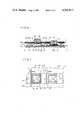
- FIG. 4is a sectional elevation view of a first example of a keyboard switch wherein, as a characteristic part of the present invention, the keyboard switch has a flexible printed circuit sheet 11, which comprises a soft flexible plastic sheet 11c, such as for example a 0.1 mm thick polyester sheet, with coatings of thermoplastic bond layers 11b and 11d. Bond layers 11b and 11d are, for example, 30 ⁇ m thick. Switch keys or buttons 11a are bonded on the upper surface of the plastic sheet 11c by means of the upper bond layer 11b, and spacers 11e are bonded on the lower surface of the plastic sheet 11c by means of the lower bond layer 11d.
- a soft flexible plastic sheet 11csuch as for example a 0.1 mm thick polyester sheet
- Bond layers 11b and 11dare, for example, 30 ⁇ m thick.
- Switch keys or buttons 11aare bonded on the upper surface of the plastic sheet 11c by means of the upper bond layer 11b
- spacers 11eare bonded on the lower surface of the plastic sheet 11c by means
- a snap action sheet 12which biases switch keys 11a upward by a resilient hemispherical convex part 12a, is provided under the plastic sheet 11c.
- Each convex part 12aincludes holes 12b through which contacts (14, 15) touch.
- the snap action sheet 12is, for example, made of a polyester insulation sheet having a resiliency by means of a number of hemispherical protrusions 12a formed by vacuum molding at positions corresponding to switch keys 11a.
- the flexible plastic sheet 11chas a second printed circuit pattern and a moving contact 14 connected thereto on the lower face thereof.
- the second printed circuit pattern and the moving contact 14are formed on the flexible plastic sheet using known conductive ink comprising metal powder, such as silver powder, and an adhesive or by means of known sputtering process.
- the switch keys 11a and the spacers 11eare simultaneously and efficiently formed by means of a specially designed mold shown in FIG. 5, wherein the mold consists of a first block 101 and a second block 102, between which the flexible plastic sheet 11c is placed (together with bonding layers 11b, and 11d).
- the first mold 101has cavities 101a for forming switch keys 11a
- the second mold 102has cavities 102a for forming spacers 11e and injecting gates 102b' connecting thereto.
- Mold 102also provides injecting gates 102b connected to the cavities 101a via through-holes 11g of the plastic sheet 11c.
- the through-holes 11gare formed beforehand, for example by a punching machine linked to an open-and-close mechanism for the mold blocks 101 and 102.
- thermoplastic materialfor example hot (about 250° C.) melted ABS is injected through the gates 102b and 102b' into cavities 101a and 102a, respectively. Since the injected melted ABS retains a temperature of around 200° C. for a short time, the portions of thermoplastic bond layers 11b and 11d contacting the injected resin in the cavities 101a and 102a are melted and bond the injected switch keys 11a and spacers 11e to flexible plastic sheet 11c. The other parts, that is, the portions of bonding layers 11b and 11d contacting the face of the mold blocks 101 and 102, are not melted.
- the integrated flexible plastic sheet 11c, switch keys 11a and spacers 11eare removed from the molds 101, 102.
- a crystalline polymer type plastic bondwhich has a nature of rapid melting over the temperature of about 130° C., is suitable as the material for the bond layers 11b and 11d.
- the bond material layers 11b and 11dselectively melt only in the vicinity of cavities 101a and 102a, respectively, wherein the high temperature plastic, (such as melted ABS) is injected, and therefore bond layers 11b and 11d do not melt and adhere to the mold blocks 101 and 102, respectively.
- plastic sheet 11cis not melted by the heat of the injected plastic, since the plastic sheet 11c is made of a high melting point plastic such as rigid saturated polyester resin. Then the hardened plastic in the gates 102b and 102b' is cut away. The plastic sheet 11c with the switch keys 11a and spacers 11e is then used in fabricating the keyboard switch of FIG. 4.
- the flexible plastic sheet 11cbends down and hence the snap action sheet 12 is pressed down.
- the pressing force on the hemispherical protrusion 12a of the snap action sheet 12exceeds a certain level, the top part of the protrusion 12a is suddenly inverted downwards, thereby allowing the switch key 11a to descend with a snap action.
- moving contact 14touches the fixed contact 15 through the opening 12b of the protrusion 12a to close a switch circuit.
- the snap action sheet 12 of insulating plastic materialserves to prevent undesirable electrical contact between portions of the first printed circuit on the flexible plastic sheet 11c and the second printed circuit on the printed circuit board 13 other than switch contacts 14 and 15.
- the snap action sheet 12By forming the snap action sheet 12 using a relatively hard, resilient plastic such as a rigid saturated polyester sheet, a distinct snap action for the switch key operation is obtainable, thereby increasing reliability of the switches.
- the end tips of the spacers 11ehave fixing pins 11f which are to be inserted through fixing holes 12d of the snap action sheet 12 and further into fixing holes 13a of the printed circuit board 13.
- the position of the snap action sheetis accurately defined with respect to the plastic sheet 11c, i.e., the upper printed circuit having moving contacts 14 and the printed circuit board 13 having the fixed contacts 15 thereon. Therefore, the relative positions of the contacts 14, 15 and the through-holes 12b of the snap action sheet 12 are accurately defined, thereby assuring reliable switching operations.
- the abovementioned structure and methodenable (1) designing very thin keyboard switches because there is no need for collar parts, (2) low manufacturing cost keyboard switches through use of a cheap resilient sheet such as polyester, (3) manufacturing the switch with a smaller number of steps and less skill because a large number of switch keys or buttons 11a are simultaneously fixed on accurate positions at the flexible plastic sheet 11c, and (4) reducing manufacturing cost by use of simple single-face printed circuit board 13 together with the flexible plastic sheet 11c with a printed circuit thereon instead of the hitherto used expensive double-face printed circuit board 3 and silicon rubber sheet 2 with contact 4 as of FIG. 1.
- FIG. 6 and FIG. 7show a second example in accordance with the present invention, wherein FIG. 6 is a sectional elevation view and FIG. 7 is a bottom view of a flexible plastic sheet 11c of FIG. 6.
- the flexible plastic sheet 11c, the switch keys 11a and spacers 11eare made in the manner elucidated in the first example referring to FIG. 5.
- the conductor of the moving contact 17 and the printed circuit formed on the lower face of the flexible plastic sheet 11care formed by a conductive rubber sheet, i.e. a thin rubber sheet containing conductive particles such as carbon black or a stable metal.
- the conductive rubber sheet 17is shaped in a circuit pattern as shown in FIG. 7 and bonded by pressing to the bond layer 11c when the latter is heated at a temperature of about 150° C.
- the bonding of the conductive rubber sheet 17can be made simultaneously with the injection molding of the switch keys 11a and spacers 11e.
- two U-shaped slits 11h and 11h'are formed on the sheet 11c in a manner to surround the area beneath the switch key 11a. Slit 11h provides greater flexibility compliance for the area bearing the moving contact 17, thereby improving the sharpness of the snap action switch operation.
- This second exampleis more economical in using the conductive rubber sheet 17 instead of silver paint as the printed circuit on the flexible plastic sheet 11c, and manifests a sharp snap action feeling.
Landscapes
- Engineering & Computer Science (AREA)
- Manufacturing & Machinery (AREA)
- Mechanical Engineering (AREA)
- Push-Button Switches (AREA)
- Manufacture Of Switches (AREA)
- Input From Keyboards Or The Like (AREA)
Abstract
Description
Claims (8)
Applications Claiming Priority (2)
| Application Number | Priority Date | Filing Date | Title |
|---|---|---|---|
| JP3119880AJPS56128523A (en) | 1980-03-11 | 1980-03-11 | Method of producing keyboard switch |
| JP55-31198 | 1980-03-11 |
Publications (1)
| Publication Number | Publication Date |
|---|---|
| US4395817Atrue US4395817A (en) | 1983-08-02 |
Family
ID=12324714
Family Applications (1)
| Application Number | Title | Priority Date | Filing Date |
|---|---|---|---|
| US06/241,040Expired - Fee RelatedUS4395817A (en) | 1980-03-11 | 1981-03-06 | Method of making keyboard switches |
Country Status (3)
| Country | Link |
|---|---|
| US (1) | US4395817A (en) |
| JP (1) | JPS56128523A (en) |
| DE (1) | DE3108183C2 (en) |
Cited By (24)
| Publication number | Priority date | Publication date | Assignee | Title |
|---|---|---|---|---|
| US4464325A (en)* | 1981-04-14 | 1984-08-07 | Nippon Gakki Seizo Kabushiki Kaisha | Method of producing multi-key structure for keyboard musical instruments |
| US4499662A (en)* | 1980-12-27 | 1985-02-19 | Sony Corporation | Injection molding method for making a switch |
| US4611261A (en)* | 1982-09-21 | 1986-09-09 | Canon Kabushiki Kaisha | Electronic equipment |
| US4764327A (en)* | 1986-01-14 | 1988-08-16 | Mitsubishi Gas Chemical Company, Inc. | Process of producing plastic-molded printed circuit boards |
| US5762852A (en)* | 1991-09-13 | 1998-06-09 | Hettinga; Siebolt | Process for making molded-in lamina hinge |
| US5811175A (en)* | 1996-01-05 | 1998-09-22 | The Grigoleit Company | Method of manufacturing a composite article having a high clarity icon and the product produced by the method |
| WO1998054045A1 (en)* | 1997-05-29 | 1998-12-03 | Yates Paul M | Bicycle seat and method of manufacture |
| US5873454A (en)* | 1996-12-06 | 1999-02-23 | Plymatech Co., Ltd. | Sheet type key top |
| US6023033A (en)* | 1996-11-29 | 2000-02-08 | Teikoku Tsushin Kogyo Co., Ltd. | Keytop plate and method for producing the same |
| US6158867A (en)* | 1996-01-16 | 2000-12-12 | Lumitex, Inc. | Light emitting panel assemblies for use in automotive applications and the like |
| USRE37687E1 (en) | 1996-01-05 | 2002-05-07 | The Grigoleit Company | Method for manufacturing an indicator knob and a knob |
| US20030043995A1 (en)* | 2001-08-31 | 2003-03-06 | Multi-National Resources | Thin film keypad and method of making same |
| US20030152660A1 (en)* | 2001-12-28 | 2003-08-14 | Webasto Vehicle Systems International Gmbh | Process and device for reinforcing a convertible soft top |
| US6667004B2 (en)* | 1995-01-26 | 2003-12-23 | La Francaise Des Plastiques | Method of forming a box or box element of plastic material |
| US20040165364A1 (en)* | 2003-02-20 | 2004-08-26 | Lg Electronics Inc. | Keypad of portable wireless terminal and fabrication method thereof |
| US7036188B1 (en) | 2004-03-24 | 2006-05-02 | The Grigoleit Company | Composite knob with light pipe leakage barrier |
| US20070221490A1 (en)* | 2006-03-23 | 2007-09-27 | Wistron Corp. | Keyboard and method for applying in-mold decoration technology to manufacture the keyboard with more key height and less key spacing |
| US20090174111A1 (en)* | 2006-04-26 | 2009-07-09 | Sunarrow Limited | Method of Manufacturing Key Top for Push Button Switch |
| EP1918953A4 (en)* | 2005-08-25 | 2011-05-04 | Nec Corp | Key inputting device and electronic device |
| US20120084966A1 (en)* | 2010-10-07 | 2012-04-12 | Microsoft Corporation | Method of making an interactive keyboard |
| EP2472544A1 (en)* | 2010-12-30 | 2012-07-04 | Research In Motion Limited | Keypad apparatus and method |
| US20120258279A1 (en)* | 2010-01-25 | 2012-10-11 | Koninklijke Philips Electronics N.V. | Method of producing a device comprising at least one displaceable operating member as well as such a device |
| US9029723B2 (en) | 2010-12-30 | 2015-05-12 | Blackberry Limited | Keypad apparatus and methods |
| US10265896B2 (en)* | 2015-04-16 | 2019-04-23 | Magna Exteriors Gmbh | Method for manufacturing a longitudinal member cladding, and a longitudinal member cladding |
Families Citing this family (8)
| Publication number | Priority date | Publication date | Assignee | Title |
|---|---|---|---|---|
| JPS6170247U (en)* | 1984-10-05 | 1986-05-14 | ||
| JPS61202830U (en)* | 1985-06-10 | 1986-12-19 | ||
| DE8610553U1 (en)* | 1986-04-17 | 1986-05-28 | Wilhelm Ruf Kg, 8000 Muenchen | Membrane keyboard |
| JPH02146725U (en)* | 1989-05-16 | 1990-12-13 | ||
| CA2022667A1 (en)* | 1989-08-09 | 1991-02-10 | Yoichi Ebina | Polybutylene terephthalate resin molded article having pictorial pattern formed thereon and process for preparing thereof |
| EP0441993A1 (en)* | 1990-02-12 | 1991-08-21 | Lexmark International, Inc. | Actuator plate for keyboard |
| DE69133364T2 (en)* | 1990-10-30 | 2004-12-09 | Teikoku Tsushin Kogyo Co. Ltd., Kawasaki | Method of making a button |
| WO2004051685A1 (en)* | 2002-12-02 | 2004-06-17 | Nissha Printing Co., Ltd. | Key sheet, method of manufacturing the key sheet, and switch product |
Citations (7)
| Publication number | Priority date | Publication date | Assignee | Title |
|---|---|---|---|---|
| US3890679A (en)* | 1973-11-09 | 1975-06-24 | Athlone Ind Inc | Garment fastener subassembly and method for making the same |
| US4033030A (en)* | 1974-09-12 | 1977-07-05 | Mohawk Data Sciences Corporation | Method of manufacturing keyswitch assemblies |
| US4057710A (en)* | 1976-03-29 | 1977-11-08 | Willmott Arthur S | Keyboard assembly |
| US4067102A (en)* | 1973-10-31 | 1978-01-10 | Essex International, Inc. | Methods of manufacturing tactile switch for keyboards and the like |
| US4131991A (en)* | 1975-10-09 | 1979-01-02 | Northern Engraving Company, Inc. | Method of making flexible pressure sensitive switch |
| GB2018024A (en) | 1978-03-17 | 1979-10-10 | Mikado Precision Ind Ltd | Electric switch |
| US4311893A (en)* | 1979-06-22 | 1982-01-19 | Citizen Watch Co., Ltd. | Push button assembly |
Family Cites Families (6)
| Publication number | Priority date | Publication date | Assignee | Title |
|---|---|---|---|---|
| JPS5322067B1 (en)* | 1967-12-08 | 1978-07-06 | ||
| JPS5137275B1 (en)* | 1971-03-11 | 1976-10-14 | ||
| JPS5024770A (en)* | 1973-07-05 | 1975-03-17 | ||
| DE2704886B2 (en)* | 1977-02-05 | 1979-04-12 | Bizerba-Werke Wilhelm Kraut Kg, 7460 Balingen | Keyboard for operating pressure switches |
| US4128744A (en)* | 1977-02-22 | 1978-12-05 | Chomerics, Inc. | Keyboard with concave and convex domes |
| JPS54101176A (en)* | 1978-01-26 | 1979-08-09 | Shinetsu Polymer Co | Contact member for push switch |
- 1980
- 1980-03-11JPJP3119880Apatent/JPS56128523A/enactivePending
- 1981
- 1981-03-04DEDE3108183Apatent/DE3108183C2/ennot_activeExpired
- 1981-03-06USUS06/241,040patent/US4395817A/ennot_activeExpired - Fee Related
Patent Citations (7)
| Publication number | Priority date | Publication date | Assignee | Title |
|---|---|---|---|---|
| US4067102A (en)* | 1973-10-31 | 1978-01-10 | Essex International, Inc. | Methods of manufacturing tactile switch for keyboards and the like |
| US3890679A (en)* | 1973-11-09 | 1975-06-24 | Athlone Ind Inc | Garment fastener subassembly and method for making the same |
| US4033030A (en)* | 1974-09-12 | 1977-07-05 | Mohawk Data Sciences Corporation | Method of manufacturing keyswitch assemblies |
| US4131991A (en)* | 1975-10-09 | 1979-01-02 | Northern Engraving Company, Inc. | Method of making flexible pressure sensitive switch |
| US4057710A (en)* | 1976-03-29 | 1977-11-08 | Willmott Arthur S | Keyboard assembly |
| GB2018024A (en) | 1978-03-17 | 1979-10-10 | Mikado Precision Ind Ltd | Electric switch |
| US4311893A (en)* | 1979-06-22 | 1982-01-19 | Citizen Watch Co., Ltd. | Push button assembly |
Cited By (36)
| Publication number | Priority date | Publication date | Assignee | Title |
|---|---|---|---|---|
| US4499662A (en)* | 1980-12-27 | 1985-02-19 | Sony Corporation | Injection molding method for making a switch |
| US4464325A (en)* | 1981-04-14 | 1984-08-07 | Nippon Gakki Seizo Kabushiki Kaisha | Method of producing multi-key structure for keyboard musical instruments |
| US4611261A (en)* | 1982-09-21 | 1986-09-09 | Canon Kabushiki Kaisha | Electronic equipment |
| US4764327A (en)* | 1986-01-14 | 1988-08-16 | Mitsubishi Gas Chemical Company, Inc. | Process of producing plastic-molded printed circuit boards |
| US5762852A (en)* | 1991-09-13 | 1998-06-09 | Hettinga; Siebolt | Process for making molded-in lamina hinge |
| US6667004B2 (en)* | 1995-01-26 | 2003-12-23 | La Francaise Des Plastiques | Method of forming a box or box element of plastic material |
| US5811175A (en)* | 1996-01-05 | 1998-09-22 | The Grigoleit Company | Method of manufacturing a composite article having a high clarity icon and the product produced by the method |
| US6568036B1 (en) | 1996-01-05 | 2003-05-27 | The Grigoleit Company | Composite indicator knob and a method for manufacturing a knob |
| US5942313A (en)* | 1996-01-05 | 1999-08-24 | The Grigoleit Company | Method of manufacturing a composite article having a high clarity icon and the product produced by the method |
| US6391243B1 (en) | 1996-01-05 | 2002-05-21 | The Grigoleit Company | Method for manufacturing an indicator knob |
| USRE37687E1 (en) | 1996-01-05 | 2002-05-07 | The Grigoleit Company | Method for manufacturing an indicator knob and a knob |
| US6158867A (en)* | 1996-01-16 | 2000-12-12 | Lumitex, Inc. | Light emitting panel assemblies for use in automotive applications and the like |
| US6367940B1 (en)* | 1996-01-16 | 2002-04-09 | Solid State Opto Limited | Light emitting panel assemblies for use in automotive applications and the like |
| US6139097A (en)* | 1996-10-16 | 2000-10-31 | Yates; Paul M. | No slip bicycle seat |
| US6023033A (en)* | 1996-11-29 | 2000-02-08 | Teikoku Tsushin Kogyo Co., Ltd. | Keytop plate and method for producing the same |
| US5873454A (en)* | 1996-12-06 | 1999-02-23 | Plymatech Co., Ltd. | Sheet type key top |
| WO1998054045A1 (en)* | 1997-05-29 | 1998-12-03 | Yates Paul M | Bicycle seat and method of manufacture |
| US20030043995A1 (en)* | 2001-08-31 | 2003-03-06 | Multi-National Resources | Thin film keypad and method of making same |
| US6821467B2 (en)* | 2001-08-31 | 2004-11-23 | Multi-National Resources | Method of making a thin film keypad |
| CN100425047C (en)* | 2001-08-31 | 2008-10-08 | 跨国资源公司 | Thin film keypad and method of making same |
| US20030152660A1 (en)* | 2001-12-28 | 2003-08-14 | Webasto Vehicle Systems International Gmbh | Process and device for reinforcing a convertible soft top |
| US20040165364A1 (en)* | 2003-02-20 | 2004-08-26 | Lg Electronics Inc. | Keypad of portable wireless terminal and fabrication method thereof |
| EP1450385A3 (en)* | 2003-02-20 | 2006-05-10 | LG Electronics Inc. | Keypad of portable wireless terminal and fabrication method thereof |
| US7277274B2 (en) | 2003-02-20 | 2007-10-02 | Lg Electronics Inc. | Keypad of portable wireless terminal and fabrication method thereof |
| US7036188B1 (en) | 2004-03-24 | 2006-05-02 | The Grigoleit Company | Composite knob with light pipe leakage barrier |
| US7203998B2 (en)* | 2004-03-24 | 2007-04-17 | The Grigoleit Company | Composite knob with light pipe leakage barrier |
| US20060156515A1 (en)* | 2004-03-24 | 2006-07-20 | Howie Robert K Jr | Composite knob with light pipe leakage barrier |
| EP1918953A4 (en)* | 2005-08-25 | 2011-05-04 | Nec Corp | Key inputting device and electronic device |
| US20070221490A1 (en)* | 2006-03-23 | 2007-09-27 | Wistron Corp. | Keyboard and method for applying in-mold decoration technology to manufacture the keyboard with more key height and less key spacing |
| US20090174111A1 (en)* | 2006-04-26 | 2009-07-09 | Sunarrow Limited | Method of Manufacturing Key Top for Push Button Switch |
| US20120258279A1 (en)* | 2010-01-25 | 2012-10-11 | Koninklijke Philips Electronics N.V. | Method of producing a device comprising at least one displaceable operating member as well as such a device |
| US9126359B2 (en)* | 2010-01-25 | 2015-09-08 | Koninklijke Philips N.V. | Method of producing a device comprising at least one displaceable operating member as well as such a device |
| US20120084966A1 (en)* | 2010-10-07 | 2012-04-12 | Microsoft Corporation | Method of making an interactive keyboard |
| EP2472544A1 (en)* | 2010-12-30 | 2012-07-04 | Research In Motion Limited | Keypad apparatus and method |
| US9029723B2 (en) | 2010-12-30 | 2015-05-12 | Blackberry Limited | Keypad apparatus and methods |
| US10265896B2 (en)* | 2015-04-16 | 2019-04-23 | Magna Exteriors Gmbh | Method for manufacturing a longitudinal member cladding, and a longitudinal member cladding |
Also Published As
| Publication number | Publication date |
|---|---|
| JPS56128523A (en) | 1981-10-08 |
| DE3108183A1 (en) | 1982-02-04 |
| DE3108183C2 (en) | 1985-09-26 |
Similar Documents
| Publication | Publication Date | Title |
|---|---|---|
| US4395817A (en) | Method of making keyboard switches | |
| KR100362027B1 (en) | Keytop plate and method for producing the same | |
| CA1154810A (en) | Tactile element and keyboard including the tactile element | |
| CN101171654B (en) | Electrically conducting contact and method for production thereof | |
| US4068369A (en) | Method of making pushbutton keyboard system | |
| CA1173480A (en) | Membrane keyboard and method of formation thereof | |
| US4929804A (en) | Push button switch | |
| US3705276A (en) | Keyboard switch assembly with conductive plastic contactor and actuator spring sleeve biasing means | |
| US4402131A (en) | Electrical switch assembly and method of manufacture | |
| US6924448B2 (en) | Movable contact unit with operating projections, method of mounting operating projections and operating panel switch using movable contact unit with operating projections | |
| JPS6220206A (en) | Push button switch and manufacture thereof | |
| US4471176A (en) | Keyboard switch | |
| EP0220275A1 (en) | Capacitance-type switch | |
| KR100463909B1 (en) | Miniaturized tact switch | |
| EP0055053B1 (en) | Electrical switch assembly and method of manufacture | |
| JP2553773Y2 (en) | Push button switch structure | |
| JP3012109U (en) | Molten resin flow confirmation device by transfer molding | |
| JP3063437B2 (en) | Push switch and method of manufacturing the same | |
| JPS61237312A (en) | Push button switch | |
| JPH0325886B2 (en) | ||
| JPH0531042U (en) | Push button switch key top | |
| KR200393119Y1 (en) | Structure of terminal of tact switch | |
| JPS63299026A (en) | Keyboard switch and its manufacture | |
| JPH031413A (en) | Push button switch | |
| JPH0448583Y2 (en) |
Legal Events
| Date | Code | Title | Description |
|---|---|---|---|
| AS | Assignment | Owner name:MATSUSHITA ELECTRIC INDUSTRIAL CO., LTD., 1006, OA Free format text:ASSIGNMENT OF ASSIGNORS INTEREST.;ASSIGNORS:ASADA TAKAFUMI;SHINOHARA KAZUYOSHI;KIYOHARA KANJI;AND OTHERS;REEL/FRAME:003875/0855 Effective date:19810224 | |
| MAFP | Maintenance fee payment | Free format text:PAYMENT OF MAINTENANCE FEE, 4TH YEAR, PL 96-517 (ORIGINAL EVENT CODE: M170); ENTITY STATUS OF PATENT OWNER: LARGE ENTITY Year of fee payment:4 | |
| MAFP | Maintenance fee payment | Free format text:PAYMENT OF MAINTENANCE FEE, 8TH YEAR, PL 96-517 (ORIGINAL EVENT CODE: M171); ENTITY STATUS OF PATENT OWNER: LARGE ENTITY Year of fee payment:8 | |
| FEPP | Fee payment procedure | Free format text:PAYOR NUMBER ASSIGNED (ORIGINAL EVENT CODE: ASPN); ENTITY STATUS OF PATENT OWNER: LARGE ENTITY | |
| FEPP | Fee payment procedure | Free format text:PAYOR NUMBER ASSIGNED (ORIGINAL EVENT CODE: ASPN); ENTITY STATUS OF PATENT OWNER: LARGE ENTITY Free format text:PAYER NUMBER DE-ASSIGNED (ORIGINAL EVENT CODE: RMPN); ENTITY STATUS OF PATENT OWNER: LARGE ENTITY | |
| FEPP | Fee payment procedure | Free format text:MAINTENANCE FEE REMINDER MAILED (ORIGINAL EVENT CODE: REM.); ENTITY STATUS OF PATENT OWNER: LARGE ENTITY | |
| LAPS | Lapse for failure to pay maintenance fees | ||
| FP | Lapsed due to failure to pay maintenance fee | Effective date:19950802 | |
| STCH | Information on status: patent discontinuation | Free format text:PATENT EXPIRED DUE TO NONPAYMENT OF MAINTENANCE FEES UNDER 37 CFR 1.362 |