US4394401A - Method of plasma enhanced chemical vapor deposition of phosphosilicate glass film - Google Patents
Method of plasma enhanced chemical vapor deposition of phosphosilicate glass filmDownload PDFInfo
- Publication number
- US4394401A US4394401AUS06/290,978US29097881AUS4394401AUS 4394401 AUS4394401 AUS 4394401AUS 29097881 AUS29097881 AUS 29097881AUS 4394401 AUS4394401 AUS 4394401A
- Authority
- US
- United States
- Prior art keywords
- sih
- mol ratio
- gas mixture
- reaction gas
- deposited
- Prior art date
- Legal status (The legal status is an assumption and is not a legal conclusion. Google has not performed a legal analysis and makes no representation as to the accuracy of the status listed.)
- Expired - Lifetime
Links
Images


Classifications
- H—ELECTRICITY
- H01—ELECTRIC ELEMENTS
- H01L—SEMICONDUCTOR DEVICES NOT COVERED BY CLASS H10
- H01L21/00—Processes or apparatus adapted for the manufacture or treatment of semiconductor or solid state devices or of parts thereof
- H01L21/02—Manufacture or treatment of semiconductor devices or of parts thereof
- H01L21/02104—Forming layers
- H01L21/02107—Forming insulating materials on a substrate
- H01L21/02109—Forming insulating materials on a substrate characterised by the type of layer, e.g. type of material, porous/non-porous, pre-cursors, mixtures or laminates
- H01L21/02112—Forming insulating materials on a substrate characterised by the type of layer, e.g. type of material, porous/non-porous, pre-cursors, mixtures or laminates characterised by the material of the layer
- H01L21/02123—Forming insulating materials on a substrate characterised by the type of layer, e.g. type of material, porous/non-porous, pre-cursors, mixtures or laminates characterised by the material of the layer the material containing silicon
- H01L21/02126—Forming insulating materials on a substrate characterised by the type of layer, e.g. type of material, porous/non-porous, pre-cursors, mixtures or laminates characterised by the material of the layer the material containing silicon the material containing Si, O, and at least one of H, N, C, F, or other non-metal elements, e.g. SiOC, SiOC:H or SiONC
- H01L21/02129—Forming insulating materials on a substrate characterised by the type of layer, e.g. type of material, porous/non-porous, pre-cursors, mixtures or laminates characterised by the material of the layer the material containing silicon the material containing Si, O, and at least one of H, N, C, F, or other non-metal elements, e.g. SiOC, SiOC:H or SiONC the material being boron or phosphorus doped silicon oxides, e.g. BPSG, BSG or PSG
- C—CHEMISTRY; METALLURGY
- C23—COATING METALLIC MATERIAL; COATING MATERIAL WITH METALLIC MATERIAL; CHEMICAL SURFACE TREATMENT; DIFFUSION TREATMENT OF METALLIC MATERIAL; COATING BY VACUUM EVAPORATION, BY SPUTTERING, BY ION IMPLANTATION OR BY CHEMICAL VAPOUR DEPOSITION, IN GENERAL; INHIBITING CORROSION OF METALLIC MATERIAL OR INCRUSTATION IN GENERAL
- C23C—COATING METALLIC MATERIAL; COATING MATERIAL WITH METALLIC MATERIAL; SURFACE TREATMENT OF METALLIC MATERIAL BY DIFFUSION INTO THE SURFACE, BY CHEMICAL CONVERSION OR SUBSTITUTION; COATING BY VACUUM EVAPORATION, BY SPUTTERING, BY ION IMPLANTATION OR BY CHEMICAL VAPOUR DEPOSITION, IN GENERAL
- C23C16/00—Chemical coating by decomposition of gaseous compounds, without leaving reaction products of surface material in the coating, i.e. chemical vapour deposition [CVD] processes
- C23C16/22—Chemical coating by decomposition of gaseous compounds, without leaving reaction products of surface material in the coating, i.e. chemical vapour deposition [CVD] processes characterised by the deposition of inorganic material, other than metallic material
- C23C16/30—Deposition of compounds, mixtures or solid solutions, e.g. borides, carbides, nitrides
- C23C16/40—Oxides
- C23C16/401—Oxides containing silicon
- C—CHEMISTRY; METALLURGY
- C23—COATING METALLIC MATERIAL; COATING MATERIAL WITH METALLIC MATERIAL; CHEMICAL SURFACE TREATMENT; DIFFUSION TREATMENT OF METALLIC MATERIAL; COATING BY VACUUM EVAPORATION, BY SPUTTERING, BY ION IMPLANTATION OR BY CHEMICAL VAPOUR DEPOSITION, IN GENERAL; INHIBITING CORROSION OF METALLIC MATERIAL OR INCRUSTATION IN GENERAL
- C23C—COATING METALLIC MATERIAL; COATING MATERIAL WITH METALLIC MATERIAL; SURFACE TREATMENT OF METALLIC MATERIAL BY DIFFUSION INTO THE SURFACE, BY CHEMICAL CONVERSION OR SUBSTITUTION; COATING BY VACUUM EVAPORATION, BY SPUTTERING, BY ION IMPLANTATION OR BY CHEMICAL VAPOUR DEPOSITION, IN GENERAL
- C23C16/00—Chemical coating by decomposition of gaseous compounds, without leaving reaction products of surface material in the coating, i.e. chemical vapour deposition [CVD] processes
- C23C16/44—Chemical coating by decomposition of gaseous compounds, without leaving reaction products of surface material in the coating, i.e. chemical vapour deposition [CVD] processes characterised by the method of coating
- C23C16/50—Chemical coating by decomposition of gaseous compounds, without leaving reaction products of surface material in the coating, i.e. chemical vapour deposition [CVD] processes characterised by the method of coating using electric discharges
- C23C16/505—Chemical coating by decomposition of gaseous compounds, without leaving reaction products of surface material in the coating, i.e. chemical vapour deposition [CVD] processes characterised by the method of coating using electric discharges using radio frequency discharges
- C23C16/509—Chemical coating by decomposition of gaseous compounds, without leaving reaction products of surface material in the coating, i.e. chemical vapour deposition [CVD] processes characterised by the method of coating using electric discharges using radio frequency discharges using internal electrodes
- C23C16/5096—Flat-bed apparatus
- H—ELECTRICITY
- H01—ELECTRIC ELEMENTS
- H01L—SEMICONDUCTOR DEVICES NOT COVERED BY CLASS H10
- H01L21/00—Processes or apparatus adapted for the manufacture or treatment of semiconductor or solid state devices or of parts thereof
- H01L21/02—Manufacture or treatment of semiconductor devices or of parts thereof
- H01L21/02104—Forming layers
- H01L21/02107—Forming insulating materials on a substrate
- H01L21/02109—Forming insulating materials on a substrate characterised by the type of layer, e.g. type of material, porous/non-porous, pre-cursors, mixtures or laminates
- H01L21/02112—Forming insulating materials on a substrate characterised by the type of layer, e.g. type of material, porous/non-porous, pre-cursors, mixtures or laminates characterised by the material of the layer
- H01L21/02123—Forming insulating materials on a substrate characterised by the type of layer, e.g. type of material, porous/non-porous, pre-cursors, mixtures or laminates characterised by the material of the layer the material containing silicon
- H01L21/02126—Forming insulating materials on a substrate characterised by the type of layer, e.g. type of material, porous/non-porous, pre-cursors, mixtures or laminates characterised by the material of the layer the material containing silicon the material containing Si, O, and at least one of H, N, C, F, or other non-metal elements, e.g. SiOC, SiOC:H or SiONC
- H—ELECTRICITY
- H01—ELECTRIC ELEMENTS
- H01L—SEMICONDUCTOR DEVICES NOT COVERED BY CLASS H10
- H01L21/00—Processes or apparatus adapted for the manufacture or treatment of semiconductor or solid state devices or of parts thereof
- H01L21/02—Manufacture or treatment of semiconductor devices or of parts thereof
- H01L21/02104—Forming layers
- H01L21/02107—Forming insulating materials on a substrate
- H01L21/02109—Forming insulating materials on a substrate characterised by the type of layer, e.g. type of material, porous/non-porous, pre-cursors, mixtures or laminates
- H01L21/02112—Forming insulating materials on a substrate characterised by the type of layer, e.g. type of material, porous/non-porous, pre-cursors, mixtures or laminates characterised by the material of the layer
- H01L21/02123—Forming insulating materials on a substrate characterised by the type of layer, e.g. type of material, porous/non-porous, pre-cursors, mixtures or laminates characterised by the material of the layer the material containing silicon
- H01L21/02164—Forming insulating materials on a substrate characterised by the type of layer, e.g. type of material, porous/non-porous, pre-cursors, mixtures or laminates characterised by the material of the layer the material containing silicon the material being a silicon oxide, e.g. SiO2
- H—ELECTRICITY
- H01—ELECTRIC ELEMENTS
- H01L—SEMICONDUCTOR DEVICES NOT COVERED BY CLASS H10
- H01L21/00—Processes or apparatus adapted for the manufacture or treatment of semiconductor or solid state devices or of parts thereof
- H01L21/02—Manufacture or treatment of semiconductor devices or of parts thereof
- H01L21/02104—Forming layers
- H01L21/02107—Forming insulating materials on a substrate
- H01L21/02225—Forming insulating materials on a substrate characterised by the process for the formation of the insulating layer
- H01L21/0226—Forming insulating materials on a substrate characterised by the process for the formation of the insulating layer formation by a deposition process
- H01L21/02263—Forming insulating materials on a substrate characterised by the process for the formation of the insulating layer formation by a deposition process deposition from the gas or vapour phase
- H01L21/02271—Forming insulating materials on a substrate characterised by the process for the formation of the insulating layer formation by a deposition process deposition from the gas or vapour phase deposition by decomposition or reaction of gaseous or vapour phase compounds, i.e. chemical vapour deposition
- H01L21/02274—Forming insulating materials on a substrate characterised by the process for the formation of the insulating layer formation by a deposition process deposition from the gas or vapour phase deposition by decomposition or reaction of gaseous or vapour phase compounds, i.e. chemical vapour deposition in the presence of a plasma [PECVD]
Definitions
- the present inventionrelates to a method of plasma enhanced chemical vapor deposition (C.V.D.) of a phosphosilicate glass (P.S.G.) film on a substrate and, more specifically, it relates to a method of plasma enhanced C.V.D of a phosphosilicate glass film on a substrate such as a silicon substrate or an aluminum wire pattern on a silicon substrate.
- C.V.D.plasma enhanced chemical vapor deposition
- P.S.G.phosphosilicate glass
- a phosphosilicate glass filmis used as a protective coating (or a cover film) or an interlaminar insulation film for wire pattern layers.
- Conventional chemical deposition methods for depositing these films on substratesare mainly classified as a so-called “atmospheric pressure method” and a so-called “low pressure method”.
- a phosphosilicate glass filmis deposited on a substrate from a reaction gas mixture including SiH 4 , PH 3 and O 2 under atmospheric pressure (i.e. 760 Torr) and at a temperature of from 350° to 450° C.
- a phosphosilicate glass filmis deposited on a substrate from a reaction gas mixture including SiH 4 , PH 3 and O 2 under a low pressure (e.g. 1 Torr) and at a temperature of from 350° to 450° C.
- a low pressuree.g. 1 Torr
- a so-called “plasma enhanced (or assisted) chemical vapor deposition method”is proposed.
- a silicon nitride film or amorphous silicon filmis deposited at a relatively low temperature (e.g. 20°-450° C.) by applying a radio frequency signal between parallel flat plate electrodes to generate plasma gas (e.g. see Electrochemical Society Meeting “Extended Abstract” 79-1, 262(1979) and Journal of Electrochemical Society 125, 601(1978)).
- an object of the present inventionis to obviate the above-mentioned problems in the conventional deposition of phosphosilicate glass films, by providing a method of plasma enhanced chemical vapor deposition of a phosphosilicate glass film on a substrate, in which phosphosilicate glass films are deposited without the generation of cracking due to a high temperature heat-treatment and without the generation of cracking due to the stress caused by cooling the deposited films to room temperature.
- a method of plasma enhanced chemical vapor deposition of a phosphosilicate glass film on a substrate from a reaction gas mixture including SiH 4 , N 2 O and PH 3is effected under conditions that the mol ratio of N 2 O to SiH 4 (N 2 O/SiH 4 ) in the reaction gas mixture is 50 or more and the mol ratio of PH 3 to SiH 4 (PH 3 /SiH 4 ) in the reaction gas mixture is 0.08 or less.
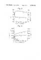
- FIG. 1is a schematic sectional view illustrating one embodiment of an apparatus for carrying out the plasma enhanced chemical vapor deposition method of the present invention
- FIG. 2is a graph illustrating a correlation between the stress of the silicon oxide and the mol ratio of N 2 O/SiH 4 in the plasma chemical vapor deposition of Example 1;
- FIG. 3is a graph illustrating a correlation between a reflection index (R.I.) of the plasma enhanced C.V.D silicon oxide films (see curve A) or the density of the silicon oxide films (see curve B) and the mol ratio of N 2 O/SiH 4 in the plasma chemical vapor deposition of Example 1;
- R.I.reflection index
- FIG. 4is a graph illustrating the correlation between an infrared absorption coefficient ⁇ of the silicon oxide film obtained in Example 1 and thermal ratio of N 2 O/SiH 4 in the plasma chemical vapor deposition of Example 1;
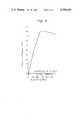
- FIG. 5is a graph illustrating the correlation between the stress of the phosphosilicate glass films deposited according to the plasma enhanced chemical vapor deposition method in Example 2 and the mol ratio of PH 3 /SiH 4 , wherein the correlation of the film according to the present invention is shown in curve A and the correlation of the film according to the conventional atmospheric pressure method is shown in curve B.
- a plasma enhanced chemical vapor deposition method of a phosphosilicate glass film (i.e. PSG film) on a substrate 11 in a bell-jar type plasma enhanced chemical vapor deposition apparatus 10will be explained in detail.
- silicon oxide filmsSi x O y , typically SiO 2
- the following procedurecan also be applied, except that a reaction gas mixture including SiH 4 , N 2 O and Ar is used in lieu of a reaction gas mixture including SiH 4 , N 2 O, PH 3 and Ar.
- a reaction gas mixture including SiH 4 , N 2 O and Aris used in lieu of a reaction gas mixture including SiH 4 , N 2 O, PH 3 and Ar.
- B 2 H 6 gas or AsH 3 gasin lieu of PH 3 gas
- a borosilicate glass film or an arsenosilicate glass filmcan be deposited on a substrate, respectively.
- a substrate 11, on which a PSG film is to be depositedis placed in a bell-jar 10 made of, for example, quartz.
- the system within the ball-jar 10is evacuated through a line 12 and the temperature of the atmosphere in the bell-jar 10 is heated to a temperature of from 20° to 450° C., preferably from 300° to 450° C., by means of a heater 13, while the pressure of the system is maintained under a vacuum pressure of from 0.1 to 2 Torr, preferably from 0.5 to 1 Torr.
- a reaction gas mixture of SiH 4 , N 2 O, PH 3 and Ar(for example, a gas mixture of 1% SiH 4 in Ar, 1% PH 3 in Ar and N 2 O) is fed through a line 14 into the bell-jar 10. Then, a PSG film is deposited on the substrate 11 by applying a radio-frequency power of from 50 KHz to 2.45 GHz (most preferably 500 KHz) by using an oscillator 15.
- the mol ratio of N 2 O/SiH 4must be 50 or more, preferably 50 through 100 and the mol ratio of PH 3 /SiH 4 must be 0.08 or less, preferably 0.03 through 0.06.
- the mol ratio of N 2 O/SiH 4is less than 50, cracking is undesirably generated in the deposited PSG film when the film is heat-treated at a high temperature.
- the mol ratio of PH 3 /SiH 4is greater than 0.08, cracking is undesirably generated in the deposited PSG film when the film is subjected to a heat-treatment at a high temperature.
- a silicon oxide film having a thickness of 1 micronwas deposited on a silicon substrate by using a plasma enhanced chemical vapor deposition apparatus as illustrated in FIG. 1.
- the plasma deposition runswere carried out by using a reaction gas mixture of SiH 4 , N 2 O and Ar under the following conditions.
- Radio frequency13.56 MHz ⁇ 40 W
- the stress of each silicon oxide film deposited at the above-mentioned N 2 O/SiH 4 ratioswas determined.
- the correlation between the determined stress values ⁇ ( ⁇ 10 8 dyne/cm) and the mol ratio of N 2 O/SiH 4is shown in FIG. 2.
- the stresswas determined according to a so-called Newton ring method.
- Samples of the silicon oxide films having a thickness of 1 micron obtained from the above-mentioned plasma enhanced chemical vapor deposition at the N 2 O/SiH 4 ratios of 5, 50 and 100were subjected to a heat-treatment at a temperature of 600° C., 800° C. or 1000° C. in a nitrogen atmosphere to observe the generation of crackin in the films.
- the resultsare shown in the following Table 1.
- the compressive stress of the deposited filmcan be offset by the tension due to the difference in the thermal expansion coefficients between the silicon substrate and the deposited silicon oxide film. As a result, no cracking is generated in the deposited silicon oxide film.
- curve Ashows the absorption coefficient (at 2240 cm -1 ) of SiH
- curve Bthe absorption coefficient (at 880 cm -1 ) of (SiH 2 )n or Si 2 O 3
- curve Cthe absorption coefficient (at 810 cm -1 ) of SiO
- curve Dthe absorption coefficient (at 1070-1090 cm -1 ) of SiO (expansion and contraction).
- the silicon oxide film obtained from the plasma enhanced chemical vapor deposition at the mol ratio of N 2 O/SiH 4 of 50 or morehas a smaller content of H 2 compared to a mol ratio which is N 2 O/SiH 4 of less than 50.
- SiH 4is thoroughly reacted with O 2 at the mol ratio of N 2 O/SiH 4 of 50 or more, whereby a silicon oxide film having good film properties can be formed.
- a phosphosilicate glass (PSG) film having a thickness of 1 micronwas deposited on a silicon substrate by using a plasma enhanced chemical vapor deposition apparatus as illustrated in FIG. 1.
- the plasma deposition runswere carried out by using a reaction gas mixture of SiH 4 , PH 3 , N 2 O and Ar under the following conditions.
- Radio-frequency13.56 MHz ⁇ 40 W
- a phosphosilicate glass film having a thickness of 1 micronwas deposited on a silicon substrate according to a conventional atmospheric pressure method.
- the deposition temperaturewas 425° C. and the deposition pressure was 760 Torr.
- the compositions of the reaction gas mixturewere SiH 4 , PH 3 , O 2 and Ar.
- the stress of each PSG film depositedwas determined in a manner as described above. The correlation between the stress ⁇ ( ⁇ 10 8 dyne/cm) and the mol ratio of PH 3 /SiH 4 is shown in curve B of FIG. 5.
- the PSG films which are under compressive stresscan be deposited on a substrate by using the mol ratio of PH 3 /SiH 4 of 0.08 or less, even in the case where the PSG film having a small concentration of phosphorous P is deposited.
- the deposited filmsare resistant to cracking.
- the PSG films having a small concentration of P and deposited by the conventional atmospheric pressure methodare under large tensile stress, cracking is likely to occur in the deposited films.
- the present inventionin the case where a PSG film having a low concentration of P and an excellent water vapor resistance (i.e. in the case where the concentration of P in the deposited film is large, phosphoric acid is formed in the film due to the absorption of H 2 O from the outside, whereby the water vapor resistance is decreased), is desired to be formed, the present invention can be effectively used.
- This type of filmis useful as a cover film, an interlaminar insulation film or the like.
Landscapes
- Chemical & Material Sciences (AREA)
- Engineering & Computer Science (AREA)
- Physics & Mathematics (AREA)
- Condensed Matter Physics & Semiconductors (AREA)
- General Physics & Mathematics (AREA)
- Manufacturing & Machinery (AREA)
- Computer Hardware Design (AREA)
- Microelectronics & Electronic Packaging (AREA)
- Power Engineering (AREA)
- General Chemical & Material Sciences (AREA)
- Chemical Kinetics & Catalysis (AREA)
- Materials Engineering (AREA)
- Mechanical Engineering (AREA)
- Metallurgy (AREA)
- Organic Chemistry (AREA)
- Plasma & Fusion (AREA)
- Inorganic Chemistry (AREA)
- Formation Of Insulating Films (AREA)
- Surface Treatment Of Glass (AREA)
- Silicon Compounds (AREA)
- Crystals, And After-Treatments Of Crystals (AREA)
- Chemical Vapour Deposition (AREA)
Abstract
Description
TABLE 1 ______________________________________ N.sub.2 O/SiH.sub.4 Heat-Treatment Temperature Ratio 600° C. 800° C. 1000° C. ______________________________________ 5 Cracking Cracking Cracking 50 No Cracking No Cracking No Cracking 100 No Cracking No Cracking No Cracking ______________________________________
Claims (10)
Applications Claiming Priority (2)
| Application Number | Priority Date | Filing Date | Title |
|---|---|---|---|
| JP55-108164 | 1980-08-08 | ||
| JP55108164AJPS5747711A (en) | 1980-08-08 | 1980-08-08 | Chemical plasma growing method in vapor phase |
Publications (1)
| Publication Number | Publication Date |
|---|---|
| US4394401Atrue US4394401A (en) | 1983-07-19 |
Family
ID=14477587
Family Applications (1)
| Application Number | Title | Priority Date | Filing Date |
|---|---|---|---|
| US06/290,978Expired - LifetimeUS4394401A (en) | 1980-08-08 | 1981-08-07 | Method of plasma enhanced chemical vapor deposition of phosphosilicate glass film |
Country Status (4)
| Country | Link |
|---|---|
| US (1) | US4394401A (en) |
| EP (1) | EP0046059B1 (en) |
| JP (1) | JPS5747711A (en) |
| DE (1) | DE3172827D1 (en) |
Cited By (29)
| Publication number | Priority date | Publication date | Assignee | Title |
|---|---|---|---|---|
| US4557950A (en)* | 1984-05-18 | 1985-12-10 | Thermco Systems, Inc. | Process for deposition of borophosphosilicate glass |
| US4612207A (en)* | 1985-01-14 | 1986-09-16 | Xerox Corporation | Apparatus and process for the fabrication of large area thin film multilayers |
| US4620986A (en)* | 1984-11-09 | 1986-11-04 | Intel Corporation | MOS rear end processing |
| US4651674A (en)* | 1984-11-16 | 1987-03-24 | Sony Corporation | Apparatus for vapor deposition |
| WO1987002828A1 (en)* | 1985-11-04 | 1987-05-07 | Motorola, Inc. | Glass intermetal dielectric |
| US5300444A (en)* | 1988-09-14 | 1994-04-05 | Mitsubishi Denki Kabushiki Kaisha | Method of manufacturing a semiconductor device having a stacked structure formed of polycrystalline silicon film and silicon oxide film |
| US5858476A (en)* | 1994-01-11 | 1999-01-12 | Siess; Harold E. | Method and apparatus for making and depositing compounds |
| US6013584A (en)* | 1997-02-19 | 2000-01-11 | Applied Materials, Inc. | Methods and apparatus for forming HDP-CVD PSG film used for advanced pre-metal dielectric layer applications |
| US6127261A (en)* | 1995-11-16 | 2000-10-03 | Advanced Micro Devices, Inc. | Method of fabricating an integrated circuit including a tri-layer pre-metal interlayer dielectric compatible with advanced CMOS technologies |
| US6194037B1 (en)* | 1995-12-28 | 2001-02-27 | Kokusai Electric Co., Ltd. | Method of plasma processing a substrate placed on a substrate table |
| US6323141B1 (en)* | 2000-04-03 | 2001-11-27 | Taiwan Semiconductor Manufacturing Company | Method for forming anti-reflective coating layer with enhanced film thickness uniformity |
| US6345589B1 (en) | 1996-03-29 | 2002-02-12 | Applied Materials, Inc. | Method and apparatus for forming a borophosphosilicate film |
| US20020182342A1 (en)* | 2001-04-13 | 2002-12-05 | Luc Ouellet | Optical quality silica films |
| US20020192393A1 (en)* | 2001-05-31 | 2002-12-19 | Luc Ouellet | Method of depositing optical films |
| US6508885B1 (en) | 1997-11-25 | 2003-01-21 | Cvc Products, Inc. | Edge sealing structure for substrate in low-pressure processing environment |
| US20030092284A1 (en)* | 2001-11-13 | 2003-05-15 | Chartered Semiconductor Manufactured Limited | Preventing plasma induced damage resulting from high density plasma deposition |
| US6627305B1 (en)* | 1997-07-16 | 2003-09-30 | Koninklijke Philips Electronics N.V. | Substrates for large area electronic devices |
| US6682981B2 (en) | 1992-04-08 | 2004-01-27 | Elm Technology Corporation | Stress controlled dielectric integrated circuit fabrication |
| US20040108071A1 (en)* | 2001-04-11 | 2004-06-10 | Thomas Wien | Label applicator and system |
| US20040192045A1 (en)* | 1992-04-08 | 2004-09-30 | Elm Technology Corporation. | Apparatus and methods for maskless pattern generation |
| US20050023656A1 (en)* | 2002-08-08 | 2005-02-03 | Leedy Glenn J. | Vertical system integration |
| US20050112806A1 (en)* | 1998-10-29 | 2005-05-26 | Kim Kwang N. | Method of forming silicon oxide layer and method of manufacturing thin film transistor thereby |
| US7138295B2 (en) | 1997-04-04 | 2006-11-21 | Elm Technology Corporation | Method of information processing using three dimensional integrated circuits |
| US7193239B2 (en) | 1997-04-04 | 2007-03-20 | Elm Technology Corporation | Three dimensional structure integrated circuit |
| US20070187803A1 (en)* | 2004-06-30 | 2007-08-16 | Intersil Americas Inc. | Plasma Enhanced Deposited, Fully Oxidized PSG Film |
| US20090215281A1 (en)* | 2008-02-22 | 2009-08-27 | Applied Materials, Inc. | Hdp-cvd sion films for gap-fill |
| CN102584019A (en)* | 2012-01-31 | 2012-07-18 | 绥中滨海经济区红杉科技有限公司 | Equipment and method for plating glass antireflective film through chemical vapor deposition process |
| US20180069119A1 (en)* | 2002-11-20 | 2018-03-08 | Renesas Electronics Corporation | Semiconductor device including gate electrode for applying tensile stress to silicon substrate, and method of manufacturing the same |
| CN108290779A (en)* | 2015-12-09 | 2018-07-17 | 法国圣戈班玻璃厂 | The method and apparatus for obtaining pane of tinted glass |
Families Citing this family (11)
| Publication number | Priority date | Publication date | Assignee | Title |
|---|---|---|---|---|
| CA1208162A (en)* | 1982-10-14 | 1986-07-22 | Dilip K. Nath | Plasma processed sinterable ceramics |
| JPH0614552B2 (en)* | 1983-02-02 | 1994-02-23 | 富士ゼロックス株式会社 | Method for manufacturing photoelectric conversion element |
| US4759993A (en)* | 1985-04-25 | 1988-07-26 | Ovonic Synthetic Materials Co., Inc. | Plasma chemical vapor deposition SiO2-x coated articles and plasma assisted chemical vapor deposition method of applying the coating |
| CA1289512C (en)* | 1985-07-29 | 1991-09-24 | Vincent D. Cannella | Depositing an electrical insulator with unidirectional gas flow in series of chambers |
| JPS6260871A (en)* | 1985-09-11 | 1987-03-17 | Anelva Corp | Vacuum chemical reaction equipment |
| JPS6362879A (en)* | 1986-09-02 | 1988-03-19 | Anelva Corp | Vacuum chemical reaction equipment |
| JPH0339475A (en)* | 1989-07-05 | 1991-02-20 | Hitachi Electron Eng Co Ltd | Method for strengthening oxide film produced in plasma CVD equipment |
| CA2006174A1 (en)* | 1989-12-20 | 1991-06-20 | Luc Ouellet | Method of making crack-free insulating films with sog interlayer |
| JPH0395922U (en)* | 1990-01-22 | 1991-09-30 | ||
| JP4711781B2 (en)* | 2005-08-29 | 2011-06-29 | 京セラ株式会社 | Thin film capacitor manufacturing method |
| JP6125176B2 (en)* | 2012-08-27 | 2017-05-10 | シャープ株式会社 | High transmittance protective film manufacturing method and semiconductor light emitting device manufacturing method |
Citations (2)
| Publication number | Priority date | Publication date | Assignee | Title |
|---|---|---|---|---|
| US4223048A (en)* | 1978-08-07 | 1980-09-16 | Pacific Western Systems | Plasma enhanced chemical vapor processing of semiconductive wafers |
| US4289797A (en)* | 1979-10-11 | 1981-09-15 | Western Electric Co., Incorporated | Method of depositing uniform films of Six Ny or Six Oy in a plasma reactor |
- 1980
- 1980-08-08JPJP55108164Apatent/JPS5747711A/enactiveGranted
- 1981
- 1981-08-05EPEP81303589Apatent/EP0046059B1/ennot_activeExpired
- 1981-08-05DEDE8181303589Tpatent/DE3172827D1/ennot_activeExpired
- 1981-08-07USUS06/290,978patent/US4394401A/ennot_activeExpired - Lifetime
Patent Citations (2)
| Publication number | Priority date | Publication date | Assignee | Title |
|---|---|---|---|---|
| US4223048A (en)* | 1978-08-07 | 1980-09-16 | Pacific Western Systems | Plasma enhanced chemical vapor processing of semiconductive wafers |
| US4289797A (en)* | 1979-10-11 | 1981-09-15 | Western Electric Co., Incorporated | Method of depositing uniform films of Six Ny or Six Oy in a plasma reactor |
Non-Patent Citations (5)
| Title |
|---|
| Electrochemical Society Meeting, "Extended Abstract", Properties of Plasma Deposited Silicon Oxide, 1979, pp. 262-265.* |
| Hallahan, "Deposition of Plasma Silicon Oxide Thin Films in a Production Planar Reactor", J. Electrochem. Soc.: Electrochemical Science and Technology, vol. 126, No. 6, Jun. 1979, pp. 930-934.* |
| Kern et al., "Advances in Deposition Processes for Passivation Films", J. Val. Sci. Technol, vol. 14, No. 5, Sep./Oct. 1977, pp. 1082-1099.* |
| Rosler et al., "Plasma Enhanced CVD in a Novel LPCVD-Type System", Solid State Technology, vol. 24, No. 4, Apr. 1981, pp. 172-177.* |
| Sinha et al., "Reactive Plasma Deposited Si-N Films for MOS-LSI Passivation", Journal of Electrochemical Society, Apr. 1978, pp. 601-608.* |
Cited By (77)
| Publication number | Priority date | Publication date | Assignee | Title |
|---|---|---|---|---|
| US4557950A (en)* | 1984-05-18 | 1985-12-10 | Thermco Systems, Inc. | Process for deposition of borophosphosilicate glass |
| US4620986A (en)* | 1984-11-09 | 1986-11-04 | Intel Corporation | MOS rear end processing |
| US4651674A (en)* | 1984-11-16 | 1987-03-24 | Sony Corporation | Apparatus for vapor deposition |
| US4612207A (en)* | 1985-01-14 | 1986-09-16 | Xerox Corporation | Apparatus and process for the fabrication of large area thin film multilayers |
| WO1987002828A1 (en)* | 1985-11-04 | 1987-05-07 | Motorola, Inc. | Glass intermetal dielectric |
| US5300444A (en)* | 1988-09-14 | 1994-04-05 | Mitsubishi Denki Kabushiki Kaisha | Method of manufacturing a semiconductor device having a stacked structure formed of polycrystalline silicon film and silicon oxide film |
| US7307020B2 (en) | 1992-04-08 | 2007-12-11 | Elm Technology Corporation | Membrane 3D IC fabrication |
| US6682981B2 (en) | 1992-04-08 | 2004-01-27 | Elm Technology Corporation | Stress controlled dielectric integrated circuit fabrication |
| US7223696B2 (en) | 1992-04-08 | 2007-05-29 | Elm Technology Corporation | Methods for maskless lithography |
| US20050156265A1 (en)* | 1992-04-08 | 2005-07-21 | Elm Technology Corporation | Lithography device for semiconductor circuit pattern generation |
| US7763948B2 (en) | 1992-04-08 | 2010-07-27 | Taiwan Semiconductor Manufacturing Co., Ltd. | Flexible and elastic dielectric integrated circuit |
| US7242012B2 (en) | 1992-04-08 | 2007-07-10 | Elm Technology Corporation | Lithography device for semiconductor circuit pattern generator |
| US7911012B2 (en) | 1992-04-08 | 2011-03-22 | Taiwan Semiconductor Manufacturing Co., Ltd. | Flexible and elastic dielectric integrated circuit |
| US7670893B2 (en) | 1992-04-08 | 2010-03-02 | Taiwan Semiconductor Manufacturing Co., Ltd. | Membrane IC fabrication |
| US7615837B2 (en) | 1992-04-08 | 2009-11-10 | Taiwan Semiconductor Manufacturing Company | Lithography device for semiconductor circuit pattern generation |
| US7550805B2 (en) | 1992-04-08 | 2009-06-23 | Elm Technology Corporation | Stress-controlled dielectric integrated circuit |
| US7485571B2 (en) | 1992-04-08 | 2009-02-03 | Elm Technology Corporation | Method of making an integrated circuit |
| US7479694B2 (en) | 1992-04-08 | 2009-01-20 | Elm Technology Corporation | Membrane 3D IC fabrication |
| US7820469B2 (en) | 1992-04-08 | 2010-10-26 | Taiwan Semiconductor Manufacturing Co., Ltd. | Stress-controlled dielectric integrated circuit |
| US7176545B2 (en) | 1992-04-08 | 2007-02-13 | Elm Technology Corporation | Apparatus and methods for maskless pattern generation |
| US6713327B2 (en)* | 1992-04-08 | 2004-03-30 | Elm Technology Corporation | Stress controlled dielectric integrated circuit fabrication |
| US7385835B2 (en) | 1992-04-08 | 2008-06-10 | Elm Technology Corporation | Membrane 3D IC fabrication |
| US20040132303A1 (en)* | 1992-04-08 | 2004-07-08 | Elm Technology Corporation | Membrane 3D IC fabrication |
| US6765279B2 (en) | 1992-04-08 | 2004-07-20 | Elm Technology Corporation | Membrane 3D IC fabrication |
| US20040150068A1 (en)* | 1992-04-08 | 2004-08-05 | Elm Technology Corporation | Membrane 3D IC fabrication |
| US20040192045A1 (en)* | 1992-04-08 | 2004-09-30 | Elm Technology Corporation. | Apparatus and methods for maskless pattern generation |
| US20050082641A1 (en)* | 1992-04-08 | 2005-04-21 | Elm Technology Corporation | Flexible and elastic dielectric integrated circuit |
| US5858476A (en)* | 1994-01-11 | 1999-01-12 | Siess; Harold E. | Method and apparatus for making and depositing compounds |
| US6127261A (en)* | 1995-11-16 | 2000-10-03 | Advanced Micro Devices, Inc. | Method of fabricating an integrated circuit including a tri-layer pre-metal interlayer dielectric compatible with advanced CMOS technologies |
| US6194037B1 (en)* | 1995-12-28 | 2001-02-27 | Kokusai Electric Co., Ltd. | Method of plasma processing a substrate placed on a substrate table |
| US6345589B1 (en) | 1996-03-29 | 2002-02-12 | Applied Materials, Inc. | Method and apparatus for forming a borophosphosilicate film |
| US6013584A (en)* | 1997-02-19 | 2000-01-11 | Applied Materials, Inc. | Methods and apparatus for forming HDP-CVD PSG film used for advanced pre-metal dielectric layer applications |
| US8841778B2 (en) | 1997-04-04 | 2014-09-23 | Glenn J Leedy | Three dimensional memory structure |
| US8928119B2 (en) | 1997-04-04 | 2015-01-06 | Glenn J. Leedy | Three dimensional structure memory |
| US7138295B2 (en) | 1997-04-04 | 2006-11-21 | Elm Technology Corporation | Method of information processing using three dimensional integrated circuits |
| US8629542B2 (en) | 1997-04-04 | 2014-01-14 | Glenn J. Leedy | Three dimensional structure memory |
| US8410617B2 (en) | 1997-04-04 | 2013-04-02 | Elm Technology | Three dimensional structure memory |
| US8318538B2 (en) | 1997-04-04 | 2012-11-27 | Elm Technology Corp. | Three dimensional structure memory |
| US8791581B2 (en) | 1997-04-04 | 2014-07-29 | Glenn J Leedy | Three dimensional structure memory |
| US8796862B2 (en) | 1997-04-04 | 2014-08-05 | Glenn J Leedy | Three dimensional memory structure |
| US8824159B2 (en) | 1997-04-04 | 2014-09-02 | Glenn J. Leedy | Three dimensional structure memory |
| US8288206B2 (en) | 1997-04-04 | 2012-10-16 | Elm Technology Corp | Three dimensional structure memory |
| US7474004B2 (en) | 1997-04-04 | 2009-01-06 | Elm Technology Corporation | Three dimensional structure memory |
| US9401183B2 (en) | 1997-04-04 | 2016-07-26 | Glenn J. Leedy | Stacked integrated memory device |
| US8907499B2 (en) | 1997-04-04 | 2014-12-09 | Glenn J Leedy | Three dimensional structure memory |
| US7504732B2 (en) | 1997-04-04 | 2009-03-17 | Elm Technology Corporation | Three dimensional structure memory |
| US9087556B2 (en) | 1997-04-04 | 2015-07-21 | Glenn J Leedy | Three dimension structure memory |
| US8035233B2 (en) | 1997-04-04 | 2011-10-11 | Elm Technology Corporation | Adjacent substantially flexible substrates having integrated circuits that are bonded together by non-polymeric layer |
| US7193239B2 (en) | 1997-04-04 | 2007-03-20 | Elm Technology Corporation | Three dimensional structure integrated circuit |
| US8933570B2 (en) | 1997-04-04 | 2015-01-13 | Elm Technology Corp. | Three dimensional structure memory |
| US7705466B2 (en) | 1997-04-04 | 2010-04-27 | Elm Technology Corporation | Three dimensional multi layer memory and control logic integrated circuit structure |
| US6627305B1 (en)* | 1997-07-16 | 2003-09-30 | Koninklijke Philips Electronics N.V. | Substrates for large area electronic devices |
| US6508885B1 (en) | 1997-11-25 | 2003-01-21 | Cvc Products, Inc. | Edge sealing structure for substrate in low-pressure processing environment |
| US7378304B2 (en)* | 1998-10-29 | 2008-05-27 | Lg.Philips Lcd Co., Ltd. | Method of forming silicon oxide layer and method of manufacturing thin film transistor thereby |
| US20050112806A1 (en)* | 1998-10-29 | 2005-05-26 | Kim Kwang N. | Method of forming silicon oxide layer and method of manufacturing thin film transistor thereby |
| US6323141B1 (en)* | 2000-04-03 | 2001-11-27 | Taiwan Semiconductor Manufacturing Company | Method for forming anti-reflective coating layer with enhanced film thickness uniformity |
| US7302982B2 (en) | 2001-04-11 | 2007-12-04 | Avery Dennison Corporation | Label applicator and system |
| US20040108071A1 (en)* | 2001-04-11 | 2004-06-10 | Thomas Wien | Label applicator and system |
| US20020182342A1 (en)* | 2001-04-13 | 2002-12-05 | Luc Ouellet | Optical quality silica films |
| EP1270762A1 (en)* | 2001-04-13 | 2003-01-02 | DALSA Semiconductor Inc. | PECVD of optical quality silica films |
| US6887514B2 (en)* | 2001-05-31 | 2005-05-03 | Dalsa Semiconductor Inc. | Method of depositing optical films |
| US20020192393A1 (en)* | 2001-05-31 | 2002-12-19 | Luc Ouellet | Method of depositing optical films |
| EP1273677A3 (en)* | 2001-05-31 | 2004-01-07 | DALSA Semiconductor Inc. | Method of depositing optical films |
| US20030092284A1 (en)* | 2001-11-13 | 2003-05-15 | Chartered Semiconductor Manufactured Limited | Preventing plasma induced damage resulting from high density plasma deposition |
| US7402897B2 (en) | 2002-08-08 | 2008-07-22 | Elm Technology Corporation | Vertical system integration |
| US20050023656A1 (en)* | 2002-08-08 | 2005-02-03 | Leedy Glenn J. | Vertical system integration |
| US8587102B2 (en) | 2002-08-08 | 2013-11-19 | Glenn J Leedy | Vertical system integration |
| US8269327B2 (en) | 2002-08-08 | 2012-09-18 | Glenn J Leedy | Vertical system integration |
| US8080442B2 (en) | 2002-08-08 | 2011-12-20 | Elm Technology Corporation | Vertical system integration |
| US20180069119A1 (en)* | 2002-11-20 | 2018-03-08 | Renesas Electronics Corporation | Semiconductor device including gate electrode for applying tensile stress to silicon substrate, and method of manufacturing the same |
| US12198987B2 (en) | 2002-11-20 | 2025-01-14 | Renesas Electronics Corporation | Semiconductor device including gate electrode for applying tensile stress to silicon substrate, and method of manufacturing the same |
| US20070187803A1 (en)* | 2004-06-30 | 2007-08-16 | Intersil Americas Inc. | Plasma Enhanced Deposited, Fully Oxidized PSG Film |
| US7704897B2 (en)* | 2008-02-22 | 2010-04-27 | Applied Materials, Inc. | HDP-CVD SiON films for gap-fill |
| US20090215281A1 (en)* | 2008-02-22 | 2009-08-27 | Applied Materials, Inc. | Hdp-cvd sion films for gap-fill |
| CN102584019B (en)* | 2012-01-31 | 2014-07-02 | 绥中滨海经济区红杉科技有限公司 | Equipment and method for plating glass antireflective film through chemical vapor deposition process |
| CN102584019A (en)* | 2012-01-31 | 2012-07-18 | 绥中滨海经济区红杉科技有限公司 | Equipment and method for plating glass antireflective film through chemical vapor deposition process |
| CN108290779A (en)* | 2015-12-09 | 2018-07-17 | 法国圣戈班玻璃厂 | The method and apparatus for obtaining pane of tinted glass |
Also Published As
| Publication number | Publication date |
|---|---|
| JPS5747711A (en) | 1982-03-18 |
| EP0046059A3 (en) | 1983-01-05 |
| DE3172827D1 (en) | 1985-12-12 |
| JPS625230B2 (en) | 1987-02-03 |
| EP0046059A2 (en) | 1982-02-17 |
| EP0046059B1 (en) | 1985-11-06 |
Similar Documents
| Publication | Publication Date | Title |
|---|---|---|
| US4394401A (en) | Method of plasma enhanced chemical vapor deposition of phosphosilicate glass film | |
| US5098865A (en) | High step coverage silicon oxide thin films | |
| Primeau et al. | The effect of thermal annealing on aerosol-gel deposited SiO2 films: a FTIR deconvolution study | |
| EP0517548B1 (en) | Chemical vapor deposition method for forming silicon oxide film | |
| US5166101A (en) | Method for forming a boron phosphorus silicate glass composite layer on a semiconductor wafer | |
| Blaauw | Stress in chemical‐vapor‐deposited SiO2 and plasma‐SiNx films on GaAs and Si | |
| KR970007839B1 (en) | Semiconductor device manufacturing method | |
| US6150258A (en) | Plasma deposited fluorinated amorphous carbon films | |
| EP0421203B1 (en) | An integrated circuit structure with a boron phosphorus silicate glass composite layer on semiconductor wafer and improved method for forming same | |
| US4795679A (en) | Monocrystalline silicon layers on substrates | |
| US4513026A (en) | Method for coating a semiconductor device with a phosphosilicate glass | |
| Hoffman et al. | Plasma‐enhanced chemical vapor deposition of silicon, germanium, and tin nitride thin films from metalorganic precursors | |
| CA2067145C (en) | Process for forming crack-free pyrolytic boron nitride on a carbon structure and article | |
| US3558348A (en) | Dielectric films for semiconductor devices | |
| US5569499A (en) | Method for reforming insulating film | |
| JPH03243770A (en) | Composite member and its production | |
| EP0794569A2 (en) | Amorphous carbon film, formation process thereof, and semiconductor device making use of the film | |
| US5786278A (en) | Method of stress-relieving silicon oxide films | |
| Templier et al. | Millitorr range PECVD of a-SiO2 films using TEOS and oxygen | |
| JPH04299515A (en) | X-ray lithography - X-ray transparent membrane for mask and method for manufacturing the same | |
| US4940851A (en) | Membrane for use in X-ray mask and method for preparing the same | |
| US4597985A (en) | Low temperature deposition of silicon oxides for device fabrication | |
| Katz et al. | Rapid thermal low‐pressure chemical vapor deposition of SiO x films onto InP | |
| JPH04362017A (en) | Formation of oriented ta2o5 thin film | |
| US5840374A (en) | Method of forming a SiO2 passivation film on a plastic substrate |
Legal Events
| Date | Code | Title | Description |
|---|---|---|---|
| AS | Assignment | Owner name:FUJITSU LIMITED, 1015, KAMIKODANAKA, NAKAHARA-KU, Free format text:ASSIGNMENT OF ASSIGNORS INTEREST.;ASSIGNORS:SHIOYA, YOSHIMI;MAEDA, MAMORU;TAKASAKI, KANETAKE;AND OTHERS;REEL/FRAME:003909/0504 Effective date:19810709 Owner name:FUJITSU LIMITED, 1015, KAMIKODANAKA, NAKAHARA-KU, Free format text:ASSIGNMENT OF ASSIGNORS INTEREST;ASSIGNORS:SHIOYA, YOSHIMI;MAEDA, MAMORU;TAKASAKI, KANETAKE;AND OTHERS;REEL/FRAME:003909/0504 Effective date:19810709 | |
| STCF | Information on status: patent grant | Free format text:PATENTED CASE | |
| CC | Certificate of correction | ||
| MAFP | Maintenance fee payment | Free format text:PAYMENT OF MAINTENANCE FEE, 4TH YEAR, PL 96-517 (ORIGINAL EVENT CODE: M170); ENTITY STATUS OF PATENT OWNER: LARGE ENTITY Year of fee payment:4 | |
| MAFP | Maintenance fee payment | Free format text:PAYMENT OF MAINTENANCE FEE, 8TH YEAR, PL 96-517 (ORIGINAL EVENT CODE: M171); ENTITY STATUS OF PATENT OWNER: LARGE ENTITY Year of fee payment:8 | |
| FEPP | Fee payment procedure | Free format text:PAYOR NUMBER ASSIGNED (ORIGINAL EVENT CODE: ASPN); ENTITY STATUS OF PATENT OWNER: LARGE ENTITY | |
| FEPP | Fee payment procedure | Free format text:PAYOR NUMBER ASSIGNED (ORIGINAL EVENT CODE: ASPN); ENTITY STATUS OF PATENT OWNER: LARGE ENTITY Free format text:PAYER NUMBER DE-ASSIGNED (ORIGINAL EVENT CODE: RMPN); ENTITY STATUS OF PATENT OWNER: LARGE ENTITY | |
| MAFP | Maintenance fee payment | Free format text:PAYMENT OF MAINTENANCE FEE, 12TH YEAR, LARGE ENTITY (ORIGINAL EVENT CODE: M185); ENTITY STATUS OF PATENT OWNER: LARGE ENTITY Year of fee payment:12 |