US4390939A - Electric power source device - Google Patents
Electric power source deviceDownload PDFInfo
- Publication number
- US4390939A US4390939AUS06/281,085US28108581AUS4390939AUS 4390939 AUS4390939 AUS 4390939AUS 28108581 AUS28108581 AUS 28108581AUS 4390939 AUS4390939 AUS 4390939A
- Authority
- US
- United States
- Prior art keywords
- circuit
- thyristors
- pulses
- circuits
- output
- Prior art date
- Legal status (The legal status is an assumption and is not a legal conclusion. Google has not performed a legal analysis and makes no representation as to the accuracy of the status listed.)
- Expired - Fee Related
Links
- 238000004804windingMethods0.000claimsdescription12
- 238000004040coloringMethods0.000abstractdescription3
- 238000004519manufacturing processMethods0.000abstractdescription3
- 230000000630rising effectEffects0.000abstract1
- 230000004044responseEffects0.000description6
- MUBZPKHOEPUJKR-UHFFFAOYSA-NOxalic acidChemical compoundOC(=O)C(O)=OMUBZPKHOEPUJKR-UHFFFAOYSA-N0.000description3
- 238000005868electrolysis reactionMethods0.000description3
- 230000016507interphaseEffects0.000description3
- PNEYBMLMFCGWSK-UHFFFAOYSA-NAluminaChemical compound[O-2].[O-2].[O-2].[Al+3].[Al+3]PNEYBMLMFCGWSK-UHFFFAOYSA-N0.000description1
- 230000004075alterationEffects0.000description1
- XAGFODPZIPBFFR-UHFFFAOYSA-NaluminiumChemical compound[Al]XAGFODPZIPBFFR-UHFFFAOYSA-N0.000description1
- 229910052782aluminiumInorganic materials0.000description1
- 230000003321amplificationEffects0.000description1
- 239000007864aqueous solutionSubstances0.000description1
- 230000015572biosynthetic processEffects0.000description1
- KRVSOGSZCMJSLX-UHFFFAOYSA-Lchromic acidSubstancesO[Cr](O)(=O)=OKRVSOGSZCMJSLX-UHFFFAOYSA-L0.000description1
- 238000010586diagramMethods0.000description1
- 230000002349favourable effectEffects0.000description1
- 238000010304firingMethods0.000description1
- AWJWCTOOIBYHON-UHFFFAOYSA-Nfuro[3,4-b]pyrazine-5,7-dioneChemical compoundC1=CN=C2C(=O)OC(=O)C2=N1AWJWCTOOIBYHON-UHFFFAOYSA-N0.000description1
- 230000004048modificationEffects0.000description1
- 238000012986modificationMethods0.000description1
- 238000003199nucleic acid amplification methodMethods0.000description1
- 235000006408oxalic acidNutrition0.000description1
Images


Classifications
- H—ELECTRICITY
- H02—GENERATION; CONVERSION OR DISTRIBUTION OF ELECTRIC POWER
- H02M—APPARATUS FOR CONVERSION BETWEEN AC AND AC, BETWEEN AC AND DC, OR BETWEEN DC AND DC, AND FOR USE WITH MAINS OR SIMILAR POWER SUPPLY SYSTEMS; CONVERSION OF DC OR AC INPUT POWER INTO SURGE OUTPUT POWER; CONTROL OR REGULATION THEREOF
- H02M1/00—Details of apparatus for conversion
- H02M1/08—Circuits specially adapted for the generation of control voltages for semiconductor devices incorporated in static converters
- H02M1/084—Circuits specially adapted for the generation of control voltages for semiconductor devices incorporated in static converters using a control circuit common to several phases of a multi-phase system
- H—ELECTRICITY
- H02—GENERATION; CONVERSION OR DISTRIBUTION OF ELECTRIC POWER
- H02M—APPARATUS FOR CONVERSION BETWEEN AC AND AC, BETWEEN AC AND DC, OR BETWEEN DC AND DC, AND FOR USE WITH MAINS OR SIMILAR POWER SUPPLY SYSTEMS; CONVERSION OF DC OR AC INPUT POWER INTO SURGE OUTPUT POWER; CONTROL OR REGULATION THEREOF
- H02M7/00—Conversion of AC power input into DC power output; Conversion of DC power input into AC power output
- H02M7/02—Conversion of AC power input into DC power output without possibility of reversal
- H02M7/04—Conversion of AC power input into DC power output without possibility of reversal by static converters
- H02M7/12—Conversion of AC power input into DC power output without possibility of reversal by static converters using discharge tubes with control electrode or semiconductor devices with control electrode
- H02M7/145—Conversion of AC power input into DC power output without possibility of reversal by static converters using discharge tubes with control electrode or semiconductor devices with control electrode using devices of a thyratron or thyristor type requiring extinguishing means
- H02M7/155—Conversion of AC power input into DC power output without possibility of reversal by static converters using discharge tubes with control electrode or semiconductor devices with control electrode using devices of a thyratron or thyristor type requiring extinguishing means using semiconductor devices only
- H02M7/162—Conversion of AC power input into DC power output without possibility of reversal by static converters using discharge tubes with control electrode or semiconductor devices with control electrode using devices of a thyratron or thyristor type requiring extinguishing means using semiconductor devices only in a bridge configuration
- H02M7/1623—Conversion of AC power input into DC power output without possibility of reversal by static converters using discharge tubes with control electrode or semiconductor devices with control electrode using devices of a thyratron or thyristor type requiring extinguishing means using semiconductor devices only in a bridge configuration with control circuit
- H02M7/1626—Conversion of AC power input into DC power output without possibility of reversal by static converters using discharge tubes with control electrode or semiconductor devices with control electrode using devices of a thyratron or thyristor type requiring extinguishing means using semiconductor devices only in a bridge configuration with control circuit with automatic control of the output voltage or current
Definitions
- This inventionrelates to electric power source devices adapted to electrolytical production or coloring of almite.
- alumiliteis produced by an electrolysis using aluminum as an anode in an aqueous solution of oxalic acid or chromic acid. It has been known in this connection that, in order to achieve a favorable film thickness or color tone of alumilite, it is necessary to reverse the direct current voltage used in the electrolysis at such comparatively high speed as, for example, 10 to 40 Hz, and the power source device must be adapted to such high speed voltage reversing.
- FIGS. 1 and 2typically such circuit as shown in FIGS. 1 and 2 has been suggested, wherein an output end is formed through a reverse parallel circuit of thyristors SCR 1 ' and SCR 2 ' in the secondary winding of a transformer T' of which the primary winding is connected to an alternating current source.
- thyristors SCR 1 ' and SCR 2 'are made to alternately conduct responsive to output pulses S 1 ' and S 2 ' of respective igniting pulse generating circuits DRV 1 ' and DRV 2 ', and high level periods T 1 ' and T 2 ' of the output pulses S 1 ' and S 2 ' are set respectively by outputs of timers TM 1 ' and TM 2 '.
- a time limiting means TM 1 "is inserted between the timer TM 1 ' and the igniting pulse generating circuit DRV 1 ' so that, after a falling of the output of the timer TM 2 ', the output of the timer TM 1 ' will not be given to the igniting pulse generating circuit DRV 1 ' during a time t 1 '.
- a time limiting means TM 2 "is inserted also between the timer TM 2 ' and the igniting pulse generating circuit DRV 2 ' so that, after a falling of the output of the timer TM 1 ', the output of the timer TM 2 ' will not be given to the igniting pulse generating circuit DRV 2 ' for a time t 2 '.
- the thyristors SCR 1 ' and SCR 2 'are made to alternately conduct with safety periods of the times t 1 ' and t 2 ' interposed and such voltage V' as shown in FIG. 2 is provided out of the output end so as to be an electric power source for the electrolysis.
- the timers, time limiting means and the likeare of a formation having contacts, so that their function as being an electric power source device has been limited, the trouble rate has been unable to be reduced and the life could not be elongated.
- the time of turning on and off the thyristors SCR 1 ' and SCR 2 'has been unable to be made shorter beyond the unit of second and thus to be more precise, they have been insufficient to be the power source device for electrolyzing alumilite.
- a primary object of the present inventionis, therefore, to provide an electric power source device wherein a control circuit having no contact is used for controlling thyristors to reduce the trouble rate and elongate the life of the device.
- Another object of the present inventionis to provide an electric power source device wherein the turning on and off operations of thyristors are made quicker and more precise so as to generate the optimum voltage for electrolytically producing alumilite.
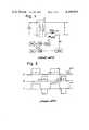
- FIG. 1, labeled PRIOR ART,shows in block diagram an example of conventional electric power source devices
- FIG. 2labeled PRIOR ART, shows voltage wave forms at respective parts in the device of FIG. 1;
- FIG. 3shows an embodiment of the electric power source device of the present invention.
- FIG. 4shows voltage wave forms at respective parts of the device shown in FIG. 3.
- Tis a transformer in which primary windings t 11 , t 12 and t 13 are inserted respectively between phases R and S, between phases S and T and between phases T and R. Secondary windings t 21 , t 22 and t 23 of the first set of the transformer T are connected at their first end with one another, and the transformer T has a second set of secondary windings t 31 , t 32 and t 33 which are also mutually connected at first end to each other.
- An interphase reactor lis inserted between respective junctions of the mutually connected first ends of the two sets of the secondary windings t 21 , t 22 and t 23 and t 31 , t 32 and t 33 .
- S 1 to S 6are rectifying units inserted respectively between second ends of the respective secondary windings t 21 , t 22 , t 23 , t 31 , t 32 and t 33 and an output terminal OT 1 , while another output terminal OT 2 is connected to the respective junctions of the first ends of the two sets of the secondary windings t 21 , t 22 and t 23 and t 31 , t 32 and t 33 respectively through the upper half part and lower half part of the interphase reactor l.
- the rectifying units S 1 to S 6respectively comprise each of reverse parallel circuits of thyristors SCR 11 and SCR 12 , SCR 21 and SCR 22 , SCR 31 and SCR 32 , SCR 41 and SCR 42 , SCR 51 and SCR 52 , and SCR 61 and SCR 62 .
- a clock signal generating circuit CLOC having an OR circuit OR 1is connected at its input ends through reversing circuits respectively to direct current ends of the respective phases of a rectifying circuit REC connected at the alternating current terminals to a three-phase alternating current source.
- a timer circuit TM including AND circuits AND 1 , AND 2 and AND 3is connected at respective one of input ends to output ends of the OR circuit OR 1 .
- An OR circuit OR 2is included in the timer circuit TM and connected at respective input ends to the output ends of the AND circuits AND 1 , AND 2 and AND 3 respectively through counters CN 1 , CN 2 and CN 3 .
- a two-stage binary counter CN 4is connected to the output end of the OR circuit OR 2 , a decoder DEC is connected at its input end to the two-stage binary counter CN 4 , at output end Q 0 to the other input end of the AND circuit AND 1 , at output ends Q 1 and Q 3 to the other input end of the AND circuit AND 2 through an OR circuit OR 3 and at output end Q 2 to the other input end of the AND circuit AND 3 .
- a phase controlling circuit CONis connected at the input end to the three-phase alternating current source and at the output end to respective gate ends of the thyristors SCR 11 through SCR 61 and of the thyristors SCR 12 through SCR 62 respectively through each of analogue switches SW 1 and SW 2 which perform an amplification of received signal and open and close operation. These switches SW 1 and SW 2 are connected at their controlling ends respectively to the output ends Q 2 and Q 0 of the decoder DEC.
- a clock signal ais provided out of the OR circuit OR 1 of the clock signal generating circuit CLOC in response to outputs of the respective phases R, S and T of the three-phase alternating current source.
- the AND circuits AND 1 , AND 2 and AND 3pass the clock signal a and provide it to the counters CN 1 , CN 2 and CN 3 during the high level periods of output signals A, B and C from the decoder DEC.
- the counters CN 1 , CN 2 and CN 3generate pulses respectively at predetermined numbers of pulses of the clock signal a.
- the pulses thus generated by the counters CN 1 , CN 2 and CN 3are added together by the OR circuit OR 2 and are given as a clock signal b to the two-stage binary counter CN 4 .
- the outputs from the output ends Q 0 and Q 1 of the two-stage binary counter CN 4are given respectively to the input ends Q A and Q B of the decoder DEC.
- the signals given to the input ends Q A and Q Bare indicated as Q A and Q B in FIG. 4.
- signals Q 0 , Q 1 , Q 2 and Q 3 as in FIG. 4are provided out of the output ends Q 0 , Q 1 , Q 2 and Q 3 of the decoder DEC.
- the decoder DECis a binary state decoder having two binary inputs Q A , Q B , wherein only the respective output Q 0 , Q 1 , Q 2 , or Q 3 , corresponding to the binary counter state or value of the binary number specified by the ordered pair (Q B , Q A ), is enabled.
- the combination of the two-state binary counter CN 4 and the binary state decoder DECfunctions as a modulo-4 counter having four decoded outputs sequentially counting from 0 to 3 with only the respectove output Q 0 , Q 1 , Q 2 , or Q 3 having a logical 1 or enabling output.
- the signals Q 1 and Q 2are added together to be the signal B in the OR circuit OR 3 and the signals Q 0 and Q 2 are directly made to be the signals A and C, respectively.
- These signals A, B and Care given respectively to the AND circuits AND.sub. 1, AND 2 and AND 3 as described above and the timer circuit TM repeats the same operation.
- the signals A and Bopen and close respectively the analogue switches SW 2 and SW 1 and give the outputs of the phase controlling circuit CON to the rectifying units S 1 to S 6 in response to the high level periods of the signals A and C.
- the thyristors SCR 11 , SCR 21 , SCR 31 , SCR 41 , SCR 51 and SCR 61 of the rectifying units S 1 to S 6are ignited sequentially by the analogue switch SW 1 while the thyristors SCR 12 , SCR 22 , SCR 32 , SCR 42 , SCR 52 and SCR 62 are ignited sequentially by the other analogue switch SW 2 .
- the thyristors SCR 11 , SCR 21 , SCR 31 , SCR 41 , SCR 51 and SCR 61are sequentially ignited in response to the high level period of the signal C and the thyristors SCR 12 , SCR 22 , SCR 32 , SCR 42 , SCR 52 and SCR 62 are sequentially ignited in response to the high level period of the signal A.
- the voltage induced in the secondary windings t 21 , t 22 , t 23 , t 31 , t 32 and t 33 of the transformer T having the primary windings t 11 , t 12 and t 13 which are connected to the three-phase alternating current sourcewill be provided as an output voltage V out of the output ends OT 1 and OT 2 through the interphase reactor l.
- the output voltage Vis a voltage of less ripples and alternately different in the polarity for the times T 1 and T 2 through the safety time t.
- the driving circuit of rectifying unitis made to have no contact so that the operation can be made quick and precise and the life can be elongated. Consequently, when the device is utilized in the electrolytic production of alumilite, the polarity reversing can be increased in number and, therefore, a high quality can be attained. In addition, in coloring alumilite, the color tone can be well secured. Further according to the present invention, the rectifying unit can be made small and light.
Landscapes
- Engineering & Computer Science (AREA)
- Power Engineering (AREA)
- Rectifiers (AREA)
Abstract
Description
Claims (4)
Applications Claiming Priority (2)
| Application Number | Priority Date | Filing Date | Title |
|---|---|---|---|
| JP55/142387 | 1980-10-14 | ||
| JP55142387AJPS5768667A (en) | 1980-10-14 | 1980-10-14 | Polarity reversal type rectifying circuit |
Publications (1)
| Publication Number | Publication Date |
|---|---|
| US4390939Atrue US4390939A (en) | 1983-06-28 |
Family
ID=15314173
Family Applications (1)
| Application Number | Title | Priority Date | Filing Date |
|---|---|---|---|
| US06/281,085Expired - Fee RelatedUS4390939A (en) | 1980-10-14 | 1981-07-07 | Electric power source device |
Country Status (5)
| Country | Link |
|---|---|
| US (1) | US4390939A (en) |
| JP (1) | JPS5768667A (en) |
| AU (1) | AU529606B2 (en) |
| CA (1) | CA1191893A (en) |
| GB (1) | GB2086154B (en) |
Cited By (2)
| Publication number | Priority date | Publication date | Assignee | Title |
|---|---|---|---|---|
| CN100336150C (en)* | 2004-11-21 | 2007-09-05 | 中国铝业股份有限公司 | Operation plate 220 V power source trip protection device |
| WO2013055455A1 (en)* | 2011-10-12 | 2013-04-18 | Thermo King Corporation | Buck-boost rectifier, refrigeration system including a buck-boost rectifier, and method of providing power to a refrigeration unit via a buck-boost rectifier |
Families Citing this family (2)
| Publication number | Priority date | Publication date | Assignee | Title |
|---|---|---|---|---|
| US5115156A (en)* | 1990-10-01 | 1992-05-19 | Tsui Huai Chou | Apparatus for triggering a plurality of thyristor devices |
| JPH04271281A (en)* | 1991-02-25 | 1992-09-28 | Sansha Electric Mfg Co Ltd | Power supply |
Citations (4)
| Publication number | Priority date | Publication date | Assignee | Title |
|---|---|---|---|---|
| US3447061A (en)* | 1965-07-12 | 1969-05-27 | Basic Inc | Multi-phase rectifier with inherent phase balance |
| US3562625A (en)* | 1965-05-04 | 1971-02-09 | Automatisme Cie Gle | Apparatus for controlling the mean value of current supplied by an alternating current source to an electric apparatus |
| US3611097A (en)* | 1970-02-05 | 1971-10-05 | Gen Electric | Digital control system for ac to dc power conversion apparatus |
| US3735241A (en)* | 1971-12-28 | 1973-05-22 | Engineering Inc T | Poly-phase digital controller |
Family Cites Families (1)
| Publication number | Priority date | Publication date | Assignee | Title |
|---|---|---|---|---|
| JPS5218376B2 (en)* | 1972-11-15 | 1977-05-21 |
- 1980
- 1980-10-14JPJP55142387Apatent/JPS5768667A/enactiveGranted
- 1981
- 1981-07-07USUS06/281,085patent/US4390939A/ennot_activeExpired - Fee Related
- 1981-07-08AUAU72648/81Apatent/AU529606B2/ennot_activeCeased
- 1981-07-15GBGB8121962Apatent/GB2086154B/ennot_activeExpired
- 1981-08-14CACA000383906Apatent/CA1191893A/ennot_activeExpired
Patent Citations (4)
| Publication number | Priority date | Publication date | Assignee | Title |
|---|---|---|---|---|
| US3562625A (en)* | 1965-05-04 | 1971-02-09 | Automatisme Cie Gle | Apparatus for controlling the mean value of current supplied by an alternating current source to an electric apparatus |
| US3447061A (en)* | 1965-07-12 | 1969-05-27 | Basic Inc | Multi-phase rectifier with inherent phase balance |
| US3611097A (en)* | 1970-02-05 | 1971-10-05 | Gen Electric | Digital control system for ac to dc power conversion apparatus |
| US3735241A (en)* | 1971-12-28 | 1973-05-22 | Engineering Inc T | Poly-phase digital controller |
Non-Patent Citations (1)
| Title |
|---|
| Oliver, "Digitally Controlled Thyristor Current Source", IEEE Transactions on Industrial Electronics and Control Instrumentation, vol. IECI-26, No. 3, Aug. 1979, pp. 185-191.* |
Cited By (3)
| Publication number | Priority date | Publication date | Assignee | Title |
|---|---|---|---|---|
| CN100336150C (en)* | 2004-11-21 | 2007-09-05 | 中国铝业股份有限公司 | Operation plate 220 V power source trip protection device |
| WO2013055455A1 (en)* | 2011-10-12 | 2013-04-18 | Thermo King Corporation | Buck-boost rectifier, refrigeration system including a buck-boost rectifier, and method of providing power to a refrigeration unit via a buck-boost rectifier |
| US8605472B2 (en) | 2011-10-12 | 2013-12-10 | Thermo King Corporation | Buck-boost rectifier, refrigeration system including a buck-boost rectifier, and method of providing power to a refrigeration unit via a buck-boost rectifier |
Also Published As
| Publication number | Publication date |
|---|---|
| GB2086154B (en) | 1984-06-20 |
| GB2086154A (en) | 1982-05-06 |
| AU7264881A (en) | 1982-06-10 |
| AU529606B2 (en) | 1983-06-16 |
| JPS5768667A (en) | 1982-04-27 |
| JPH0526430B2 (en) | 1993-04-16 |
| CA1191893A (en) | 1985-08-13 |
Similar Documents
| Publication | Publication Date | Title |
|---|---|---|
| US3950657A (en) | Timer circuits | |
| US3805141A (en) | Bimodal inverter | |
| GB1083530A (en) | Improvements in or relating to an inverter | |
| US4390939A (en) | Electric power source device | |
| US4833284A (en) | Power relay switching control device for microwave oven | |
| US4030019A (en) | Static inverter control circuit | |
| RU17383U1 (en) | DEVICE FOR CONTROL OF VIBRATOR ELECTRIC MOTOR | |
| SU1307521A1 (en) | Multimotor a.c.electric drive | |
| US3406329A (en) | Parallel inverter with rapid response time to changes in pulse durations | |
| RU2296457C2 (en) | Apparatus for magnetic-pulsed treatment of plants | |
| SU512547A1 (en) | Constant voltage to ac converter | |
| SU875580A1 (en) | Method of starting thyristorized voltage inverter | |
| SU1107234A1 (en) | A.c. voltage-to-a.c. voltage converter for testing installations | |
| KR100274471B1 (en) | Current Inverting Rectifier | |
| SU1307515A1 (en) | Variable a.c.voltage-to-a.c.voltage converter | |
| SU1511831A1 (en) | Method and apparatus for switching over control windings of reactor | |
| SU1464270A1 (en) | Power regulating device | |
| SU811484A1 (en) | Method of control of reversible thyristorized pulse power amplifier | |
| SU1658364A1 (en) | Device for controlling multiphase stepped motor | |
| SU1672566A1 (en) | Converter of digital code to pulse sequence | |
| SU1181096A1 (en) | A.c.voltage-to-d.c.voltage converter | |
| SU596664A1 (en) | Device for electrochemical processing of articles with asymmetric current | |
| US3486121A (en) | Timing circuit providing prearranged sequences of output pulses | |
| SU1465989A1 (en) | Electronic switching unit for a.c. network | |
| SU1735991A1 (en) | Control gear for three-phase induction motor |
Legal Events
| Date | Code | Title | Description |
|---|---|---|---|
| AS | Assignment | Owner name:KABUSHIKI KAISHA CHIYODA,TOKYO, JAPAN A CORP. OF J Free format text:ASSIGNMENT OF ASSIGNORS INTEREST.;ASSIGNOR:SUGAWARA, ISAO;REEL/FRAME:003923/0440 Effective date:19810624 | |
| AS | Assignment | Owner name:KABUSHIKI KAISHA CHIYODA 24-10, CHUO 4-CHOME, WARA Free format text:STATEMENT BY ASSIGNEE SHOWING CHANGE OF ADDRESS;ASSIGNOR:KABUSHIKI KAISHA CHIYODA 17-4, NAKAZATO 3-CHOME, KITA-KU, TOKYO, JAPAN;REEL/FRAME:004316/0897 Effective date:19841003 Owner name:KABUSHIKI KAISHA CHIYODA,JAPAN Free format text:STATEMENT BY ASSIGNEE SHOWING CHANGE OF ADDRESS;ASSIGNOR:KABUSHIKI KAISHA CHIYODA 17-4, NAKAZATO 3-CHOME, KITA-KU, TOKYO, JAPAN;REEL/FRAME:004316/0897 Effective date:19841003 | |
| MAFP | Maintenance fee payment | Free format text:PAYMENT OF MAINTENANCE FEE, 4TH YEAR, PL 96-517 (ORIGINAL EVENT CODE: M170); ENTITY STATUS OF PATENT OWNER: LARGE ENTITY Year of fee payment:4 | |
| FEPP | Fee payment procedure | Free format text:PAYOR NUMBER ASSIGNED (ORIGINAL EVENT CODE: ASPN); ENTITY STATUS OF PATENT OWNER: LARGE ENTITY | |
| MAFP | Maintenance fee payment | Free format text:PAYMENT OF MAINTENANCE FEE, 8TH YEAR, PL 96-517 (ORIGINAL EVENT CODE: M171); ENTITY STATUS OF PATENT OWNER: LARGE ENTITY Year of fee payment:8 | |
| FEPP | Fee payment procedure | Free format text:MAINTENANCE FEE REMINDER MAILED (ORIGINAL EVENT CODE: REM.); ENTITY STATUS OF PATENT OWNER: LARGE ENTITY | |
| LAPS | Lapse for failure to pay maintenance fees | ||
| FP | Lapsed due to failure to pay maintenance fee | Effective date:19950628 | |
| STCH | Information on status: patent discontinuation | Free format text:PATENT EXPIRED DUE TO NONPAYMENT OF MAINTENANCE FEES UNDER 37 CFR 1.362 |