US4389429A - Method of forming integrated circuit chip transmission line - Google Patents
Method of forming integrated circuit chip transmission lineDownload PDFInfo
- Publication number
- US4389429A US4389429AUS06/393,149US39314982AUS4389429AUS 4389429 AUS4389429 AUS 4389429AUS 39314982 AUS39314982 AUS 39314982AUS 4389429 AUS4389429 AUS 4389429A
- Authority
- US
- United States
- Prior art keywords
- substrate
- conductor
- layer
- silicon
- etch
- Prior art date
- Legal status (The legal status is an assumption and is not a legal conclusion. Google has not performed a legal analysis and makes no representation as to the accuracy of the status listed.)
- Expired - Lifetime
Links
Images


Classifications
- H—ELECTRICITY
- H01—ELECTRIC ELEMENTS
- H01L—SEMICONDUCTOR DEVICES NOT COVERED BY CLASS H10
- H01L23/00—Details of semiconductor or other solid state devices
- H01L23/52—Arrangements for conducting electric current within the device in operation from one component to another, i.e. interconnections, e.g. wires, lead frames
- H01L23/522—Arrangements for conducting electric current within the device in operation from one component to another, i.e. interconnections, e.g. wires, lead frames including external interconnections consisting of a multilayer structure of conductive and insulating layers inseparably formed on the semiconductor body
- H01L23/5221—Crossover interconnections
- H—ELECTRICITY
- H01—ELECTRIC ELEMENTS
- H01L—SEMICONDUCTOR DEVICES NOT COVERED BY CLASS H10
- H01L21/00—Processes or apparatus adapted for the manufacture or treatment of semiconductor or solid state devices or of parts thereof
- H01L21/70—Manufacture or treatment of devices consisting of a plurality of solid state components formed in or on a common substrate or of parts thereof; Manufacture of integrated circuit devices or of parts thereof
- H01L21/71—Manufacture of specific parts of devices defined in group H01L21/70
- H01L21/768—Applying interconnections to be used for carrying current between separate components within a device comprising conductors and dielectrics
- H01L21/76801—Applying interconnections to be used for carrying current between separate components within a device comprising conductors and dielectrics characterised by the formation and the after-treatment of the dielectrics, e.g. smoothing
- H01L21/7682—Applying interconnections to be used for carrying current between separate components within a device comprising conductors and dielectrics characterised by the formation and the after-treatment of the dielectrics, e.g. smoothing the dielectric comprising air gaps
- H—ELECTRICITY
- H01—ELECTRIC ELEMENTS
- H01L—SEMICONDUCTOR DEVICES NOT COVERED BY CLASS H10
- H01L23/00—Details of semiconductor or other solid state devices
- H01L23/52—Arrangements for conducting electric current within the device in operation from one component to another, i.e. interconnections, e.g. wires, lead frames
- H01L23/535—Arrangements for conducting electric current within the device in operation from one component to another, i.e. interconnections, e.g. wires, lead frames including internal interconnections, e.g. cross-under constructions
- H—ELECTRICITY
- H01—ELECTRIC ELEMENTS
- H01L—SEMICONDUCTOR DEVICES NOT COVERED BY CLASS H10
- H01L2924/00—Indexing scheme for arrangements or methods for connecting or disconnecting semiconductor or solid-state bodies as covered by H01L24/00
- H01L2924/0001—Technical content checked by a classifier
- H01L2924/0002—Not covered by any one of groups H01L24/00, H01L24/00 and H01L2224/00
Definitions
- This inventionrelates to the field of establishing relatively long interconnections on integrated chips while reducing the RC time constant of such connections over present day connections.
- the methodrelates to the selective etching into a semiconductor substrate to isolate at least one elongated portion of a conductive coating to define a first conductor, and applying a further conductive coating to the etched substrate to comprise a second conductor in spaced relation to the first conductor.
- Thismay be achieved by using an orientation dependent etchant to provide a V-shaped groove with the first conductor in the mouth of the V.
- the substratemay have an elongated cavity etched therein from one side with a first conductor disposed in the mouth of the cavity and a second conductor coating the cavity; with the first conductor extending via a pyramidal pit through an etched hole to make contact with a metallization pattern.
- the apparatuscomprises the completed product.
- FIG. 1shows the metallization of the silicon
- FIG. 2discloses patterning of the photo resist
- FIG. 3shows the removal of the metal from the unprotected areas
- FIG. 4shows an etching step which removes silicon to leave a metal conductor in the mouth of the cavity so formed
- FIG. 5shows the addition of metallization to the cavity
- FIG. 6shows a similar patterning step for a silicon substrate which has been metallized and patterned with photoresist
- FIG. 7shows the etching of a V-shaped groove or cavity through the use of orientation dependent etchant
- FIG. 8shows the structure with a metallization coating applied to the V-shaped groove
- FIG. 9shows the structure in perspective, better to illustrate the supporting of the central conductor
- FIG. 10shows the initial doping of a substrate for use in an arrangement utilizing both sides of the substrate for the transmission lines
- FIG. 11shows the addition of an epi-layer for the integrated circuit processing in normal manner
- FIG. 12shows the back side of the wafer as a P+ diffused layer
- FIG. 13shows the use of an orientation dependent etchant to develop the V groove from the reverse side of the substrate
- FIG. 14shows metallization applied to both sides of the substrate and in connection therewith through the etch pit.
- FIG. 15is a perspective view from the rear side of the substrate, showing the center conductor connected via the pyramidal metallized etch pit to the front side of the substrate.
- the purpose of the inventionis to avoid the serious circuit performance problems due to the relatively large capacitance per unit area and the large resistant per unit length encountered in the longer interconnections used in high speed integrated circuit chips.
- the large resistance per unit lengthis in part the result of the current return path in the silicon substrate.
- the combination of the large resistance and capacitanceresults in a large circuit time constant. This produces a large amount of signal attenuation, signal distortion, and a long propagation delay time.
- the subject arrangementproduces long range innerconnections on an integrated chip having a much lower capacitance and resistance per unit length.
- the primary loss mechanism for the conventional MOS type of innerconnection on silicon integrated chipsis due to the RC time constant, wherein the capacitance can be reduced as well as the resistance by use of the constructions shown in the ensuing figures.
- the capacitanceis reduced as a result of the change from the silicon dioxide/silicon dielectric structure with dielectric constants of 3.8 and 11.8, respectively to air with the dielectric constant of 1. Also, the spacing is increased between the effective "plates.”
- the resistanceis decreased i.e. series resistance by changing from silicon for the bottom (substrate) conductor with 0.01 to 1 ohm-centimeter resistivity to aluminum with approximately 3 micro ohms-centimeter resistivity.
- the shunt conductanceis reduced from that due to the conductivity of silicon down to essentially zero i.e. the air dielectric.
- the short range metallization innerconnectionsi.e., approximately 10 mils or less are accomplished in the usual processing of the IC side of the wafer.
- the long range metallizationi.e. about 100 mils or greater may be accomplished on the back side of the wafer as described herein.
- groovesare etched on the back side of the wafer for the long range metallization.
- the back sideis then subjected to a second metallization plus photoresist operation to produce a metallic coating inside the grooves and to build up the thickness of the center conductor.
- the back sidemay be almost fully metallized except for the small gaps required in the region of the etched through pyramid etched pits for electrical separation of contacts to the beam conductors from the substrate ground-plane. The latter reduces the parasitic substrate resistance, which is a problem in conventional structure due to the RC time constants, feedback effects and crosstalk when there is all top contacts and no back surface metallization.
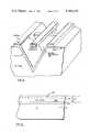
- FIG. 1a silicon substrate 11 is covered with a layer of metal (e.g.) aluminum 13.
- a patterned photoresist 15is applied over the aluminum 13, as shown in FIG. 2 and etching takes place in FIG. 3. It will be seen that not only is the aluminum layer 13 etched but also slots are etched into the silicon 11. Alternately, of course, ion milling could be employed in lieu of the etching. From FIG. 4 it may be seen that the process step of FIG. 3 merely defined the central aluminum conductor 17 which appears to be floating above the cavity 19 formed in the silicon 11 by etching the silicon further and then removing the photoresist 15.
- FIG. 5shows the structure of FIG. 4 with further aluminum deposited to coat the cavity 19 boundaries and also build up the conductor 17.
- a slight depression 21is shown beneath the aluminum beneath 17 due to the shielding of the beam 17 from the source of aluminum for deposit.
- one conductormay be beam 17 and the other coating 20 with an air dielectric therebetween, thereby reducing both the capacitive and resistive effects of this transmission line.
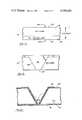
- FIGS. 6 through 8A second embodiment of the invention is shown in FIGS. 6 through 8 wherein again the photoresist pattern is laid down on the silicon substrate 11 with the photoresist shown at 15 and the aluminum coating at 13.
- FIG. 8the photoresist 15 has been removed and metallization, including such material as aluminum has been deposited to line the V-shaped groove, as shown at 20.
- the aluminum depositionis done in an evaporator in which the aluminum evaporant flux is incident on the silicon wafers over a wide angular spread. This provides for a more uniform coating 20.
- the aluminum beam 17may be supported by silicon ridges at the ends or by intermediate webs of silicon.
- FIG. 9This is better shown in FIG. 9 in the perspective view wherein the beam 17 is shown atop a silicon supporting web 31.
- the web 31was protected by photoresist in the processing previously described.
- the structure of FIG. 9may be rotated about the source of aluminum in order to provide more uniform coating.
- the V groove coaxial metallizationcan be placed on the back side of the chip.
- the starting materialis a (100) silicon substrate 101 e.g. P-type 1 of FIG. 10. This is of light to moderate doping and typically about 5 to 10 mils thick. A high concentration P+ diffusion is performed into this substrate and P+ layer on one side will be etched off, leaving a P+ over P structure, as shown.
- the P siliconremains and is shown at 101, and the P+ at 103.
- the P+ regionmay have a thickness of approximately 1 to 10 micrometers whereas the overall substrate thickness may be of the order of 5 to 10 mils.
- an epi-layer about 10 to 20 micrometers thick as shown at 105is deposited on the P+ over P substrate and the normal I.C. processing is then undertaken to produce the I.C. circuit in the epi-layer as indicated at 105'.
- the region 105'is the complete I.C. circuitry but excluding the long range metallization pattern.
- the I.C. waferis then subjected to a concentration dependent etchant with the I.C. side of the wafer coated with an etch resistant layer.
- a concentration dependent etchantwith the I.C. side of the wafer coated with an etch resistant layer.
- the P type substrate 101is etched away but the P+ diffused layer serves as an etch stop, as seen in FIG. 12.
- the resulting wafer 111is thinned down as shown in FIG. 12.
- the processingtakes place on the back side of the wafer 111 and includes a conventional photoresist step using infrared illumination registration purposes to provide a series of square shaped openings in the P.R. layer.
- the front side of the wafer 105"is coated with an etch resistant layer.
- the back side 103' of wafer 112is subjected to an orientation dependent etchant which etches the (111) planes at a rate much slower than the (100) planes.
- the etchingproceeds through the wafer thickness to the top side, as shown in FIG. 13.
- FIG. 13A cross section of such a pit 121 is shown in FIG. 13. It includes a square opening 123 in the bottom of the wafer 112 and a square opening 125 in the top of the wafer 112.
- An oxide layer 129is then grown (or deposited) on both sides of the wafer, as shown in FIG. 14.
- the metallization layer 131is then deposited and defined by a photoresist process on both sides of the wafer so that contact is made through the etch hole 123 between the two sides of the wafer, as shown in FIG. 14. Thus contact is made through the etch hole 123 between the two sides of the wafer.
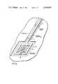
- FIG. 15a perspective view shows the overall structure including the central conductor 17 supported by the silicon webs 31.
- Conductor 17extends in metallization contact down through pyramidal etch pit 125 and out the lower square opening 123 to join the front conductor metallization. In this manner, the conductors may penetrate the wafer and the return path may extend along the back side of the wafer but not in silicon form rather in metallization form.
Landscapes
- Engineering & Computer Science (AREA)
- Physics & Mathematics (AREA)
- Condensed Matter Physics & Semiconductors (AREA)
- General Physics & Mathematics (AREA)
- Computer Hardware Design (AREA)
- Microelectronics & Electronic Packaging (AREA)
- Power Engineering (AREA)
- Manufacturing & Machinery (AREA)
- Weting (AREA)
Abstract
Description
Claims (5)
Priority Applications (1)
| Application Number | Priority Date | Filing Date | Title |
|---|---|---|---|
| US06/393,149US4389429A (en) | 1980-06-16 | 1982-06-28 | Method of forming integrated circuit chip transmission line |
Applications Claiming Priority (2)
| Application Number | Priority Date | Filing Date | Title |
|---|---|---|---|
| US06/160,031US4379307A (en) | 1980-06-16 | 1980-06-16 | Integrated circuit chip transmission line |
| US06/393,149US4389429A (en) | 1980-06-16 | 1982-06-28 | Method of forming integrated circuit chip transmission line |
Related Parent Applications (1)
| Application Number | Title | Priority Date | Filing Date |
|---|---|---|---|
| US06/160,031DivisionUS4379307A (en) | 1980-06-16 | 1980-06-16 | Integrated circuit chip transmission line |
Publications (1)
| Publication Number | Publication Date |
|---|---|
| US4389429Atrue US4389429A (en) | 1983-06-21 |
Family
ID=26856541
Family Applications (1)
| Application Number | Title | Priority Date | Filing Date |
|---|---|---|---|
| US06/393,149Expired - LifetimeUS4389429A (en) | 1980-06-16 | 1982-06-28 | Method of forming integrated circuit chip transmission line |
Country Status (1)
| Country | Link |
|---|---|
| US (1) | US4389429A (en) |
Cited By (32)
| Publication number | Priority date | Publication date | Assignee | Title |
|---|---|---|---|---|
| US4472239A (en)* | 1981-10-09 | 1984-09-18 | Honeywell, Inc. | Method of making semiconductor device |
| EP0181600A3 (en)* | 1984-11-14 | 1987-03-11 | Kabushiki Kaisha Toshiba | Signal transmission circuit in a semiconductor integrated circuit |
| US4682503A (en)* | 1986-05-16 | 1987-07-28 | Honeywell Inc. | Microscopic size, thermal conductivity type, air or gas absolute pressure sensor |
| US4724356A (en)* | 1986-10-10 | 1988-02-09 | Lockheed Missiles & Space Co., Inc. | Infrared display device |
| US4776087A (en)* | 1987-04-27 | 1988-10-11 | International Business Machines Corporation | VLSI coaxial wiring structure |
| US4849069A (en)* | 1986-12-13 | 1989-07-18 | Spectrol Reliance Limited | Method of producing filaments |
| US4875971A (en)* | 1987-04-05 | 1989-10-24 | Elron Electronic Industries, Ltd. | Fabrication of customized integrated circuits |
| US4924287A (en)* | 1985-01-20 | 1990-05-08 | Avner Pdahtzur | Personalizable CMOS gate array device and technique |
| US5053105A (en)* | 1990-07-19 | 1991-10-01 | Micron Technology, Inc. | Process for creating an etch mask suitable for deep plasma etches employing self-aligned silicidation of a metal layer masked with a silicon dioxide template |
| US5348617A (en)* | 1991-12-23 | 1994-09-20 | Iowa State University Research Foundation, Inc. | Selective etching process |
| US5601687A (en)* | 1995-09-11 | 1997-02-11 | The United States Of America As Represented By The Secretary Of The Air Force | Mask design |
| US5891797A (en)* | 1997-10-20 | 1999-04-06 | Micron Technology, Inc. | Method of forming a support structure for air bridge wiring of an integrated circuit |
| US20020037603A1 (en)* | 2000-08-16 | 2002-03-28 | Eldridge Jerome M. | Microelectronic device package with conductive elements and associated method of manufacture |
| US20020098677A1 (en)* | 2000-05-31 | 2002-07-25 | Micron Technology, Inc. | Multilevel copper interconnects with low-k dielectrics and air gaps |
| US6509590B1 (en) | 1998-07-20 | 2003-01-21 | Micron Technology, Inc. | Aluminum-beryllium alloys for air bridges |
| US6620638B1 (en) | 2002-06-05 | 2003-09-16 | Micron Technology, Inc. | Testing of multi-chip electronic modules |
| US6670719B2 (en) | 1999-08-25 | 2003-12-30 | Micron Technology, Inc. | Microelectronic device package filled with liquid or pressurized gas and associated method of manufacture |
| US6686654B2 (en) | 2001-08-31 | 2004-02-03 | Micron Technology, Inc. | Multiple chip stack structure and cooling system |
| US6747347B2 (en) | 2001-08-30 | 2004-06-08 | Micron Technology, Inc. | Multi-chip electronic package and cooling system |
| US20040113385A1 (en)* | 2002-11-28 | 2004-06-17 | Shimano, Inc. | Bicycle electronic control device with a reset function |
| US20040206308A1 (en)* | 2000-01-18 | 2004-10-21 | Micron Technologies, Inc. | Methods and apparatus for making integrated-circuit wiring from copper, silver, gold, and other metals |
| US20050026351A1 (en)* | 1999-08-25 | 2005-02-03 | Micron Technology, Inc. | Packaging of electronic chips with air-bridge structures |
| US20050112871A1 (en)* | 2000-05-31 | 2005-05-26 | Micron Technology, Inc. | Multilevel copper interconnect with double passivation |
| US20050181392A1 (en)* | 2000-02-29 | 2005-08-18 | Stmicroelectronics S.R.L. | Integrated chemical microreactor with large area channels and manufacturing process thereof |
| US20060046322A1 (en)* | 2004-08-31 | 2006-03-02 | Micron Technology, Inc. | Integrated circuit cooling and insulating device and method |
| US7262505B2 (en) | 2000-01-18 | 2007-08-28 | Micron Technology, Inc. | Selective electroless-plated copper metallization |
| US20070252224A1 (en)* | 2000-02-29 | 2007-11-01 | Stmicroelectronics S.R.L. | Integrated Chemical Microreactor With Large Area Channels and Manufacturing Process Thereof |
| US7402516B2 (en) | 2000-01-18 | 2008-07-22 | Micron Technology, Inc. | Method for making integrated circuits |
| US7465608B1 (en) | 2001-08-17 | 2008-12-16 | Micron Technology, Inc. | Three-dimensional multichip module |
| WO2012125898A1 (en)* | 2011-03-17 | 2012-09-20 | Georgia Tech Research Corporation | Patterned graphene structures on silicon carbide |
| US8779596B2 (en) | 2000-01-18 | 2014-07-15 | Micron Technology, Inc. | Structures and methods to enhance copper metallization |
| US9171907B2 (en) | 2011-09-27 | 2015-10-27 | Georgia Tech Research Corporation | Graphene transistor |
Citations (2)
| Publication number | Priority date | Publication date | Assignee | Title |
|---|---|---|---|---|
| US3813585A (en)* | 1970-04-28 | 1974-05-28 | Agency Ind Science Techn | Compound semiconductor device having undercut oriented groove |
| US4312117A (en)* | 1977-09-01 | 1982-01-26 | Raytheon Company | Integrated test and assembly device |
- 1982
- 1982-06-28USUS06/393,149patent/US4389429A/ennot_activeExpired - Lifetime
Patent Citations (2)
| Publication number | Priority date | Publication date | Assignee | Title |
|---|---|---|---|---|
| US3813585A (en)* | 1970-04-28 | 1974-05-28 | Agency Ind Science Techn | Compound semiconductor device having undercut oriented groove |
| US4312117A (en)* | 1977-09-01 | 1982-01-26 | Raytheon Company | Integrated test and assembly device |
Cited By (67)
| Publication number | Priority date | Publication date | Assignee | Title |
|---|---|---|---|---|
| US4472239A (en)* | 1981-10-09 | 1984-09-18 | Honeywell, Inc. | Method of making semiconductor device |
| EP0181600A3 (en)* | 1984-11-14 | 1987-03-11 | Kabushiki Kaisha Toshiba | Signal transmission circuit in a semiconductor integrated circuit |
| US4687949A (en)* | 1984-11-14 | 1987-08-18 | Kabushiki Kaisha Toshiba | Signal transmission circuit in a semiconductor integrated circuit |
| US4924287A (en)* | 1985-01-20 | 1990-05-08 | Avner Pdahtzur | Personalizable CMOS gate array device and technique |
| US4682503A (en)* | 1986-05-16 | 1987-07-28 | Honeywell Inc. | Microscopic size, thermal conductivity type, air or gas absolute pressure sensor |
| US4724356A (en)* | 1986-10-10 | 1988-02-09 | Lockheed Missiles & Space Co., Inc. | Infrared display device |
| US4849069A (en)* | 1986-12-13 | 1989-07-18 | Spectrol Reliance Limited | Method of producing filaments |
| US4875971A (en)* | 1987-04-05 | 1989-10-24 | Elron Electronic Industries, Ltd. | Fabrication of customized integrated circuits |
| US4776087A (en)* | 1987-04-27 | 1988-10-11 | International Business Machines Corporation | VLSI coaxial wiring structure |
| US5053105A (en)* | 1990-07-19 | 1991-10-01 | Micron Technology, Inc. | Process for creating an etch mask suitable for deep plasma etches employing self-aligned silicidation of a metal layer masked with a silicon dioxide template |
| US5348617A (en)* | 1991-12-23 | 1994-09-20 | Iowa State University Research Foundation, Inc. | Selective etching process |
| US5601687A (en)* | 1995-09-11 | 1997-02-11 | The United States Of America As Represented By The Secretary Of The Air Force | Mask design |
| US5891797A (en)* | 1997-10-20 | 1999-04-06 | Micron Technology, Inc. | Method of forming a support structure for air bridge wiring of an integrated circuit |
| US5994777A (en)* | 1997-10-20 | 1999-11-30 | Micron Technology, Inc. | Method and support structure for air bridge wiring of an integrated circuit |
| US20030127741A1 (en)* | 1998-07-20 | 2003-07-10 | Micron Technology, Inc. | Aluminum-beryllium alloys for air bridges |
| US6509590B1 (en) | 1998-07-20 | 2003-01-21 | Micron Technology, Inc. | Aluminum-beryllium alloys for air bridges |
| US20040192020A1 (en)* | 1998-07-20 | 2004-09-30 | Micron Technology, Inc. | Aluminum-beryllium alloys for air bridges |
| US6943090B2 (en) | 1998-07-20 | 2005-09-13 | Micron Technology, Inc. | Aluminum-beryllium alloys for air bridges |
| US6717191B2 (en) | 1998-07-20 | 2004-04-06 | Micron Technology, Inc. | Aluminum-beryllium alloys for air bridges |
| US7335965B2 (en) | 1999-08-25 | 2008-02-26 | Micron Technology, Inc. | Packaging of electronic chips with air-bridge structures |
| US7387912B2 (en) | 1999-08-25 | 2008-06-17 | Micron Technology, Inc. | Packaging of electronic chips with air-bridge structures |
| US20070042595A1 (en)* | 1999-08-25 | 2007-02-22 | Micron Technology, Inc. | Packaging of electronic chips with air-bridge structures |
| US6670719B2 (en) | 1999-08-25 | 2003-12-30 | Micron Technology, Inc. | Microelectronic device package filled with liquid or pressurized gas and associated method of manufacture |
| US20060244112A1 (en)* | 1999-08-25 | 2006-11-02 | Micron Technology, Inc. | Packaging of electronic chips with air-bridge structures |
| US20050285220A1 (en)* | 1999-08-25 | 2005-12-29 | Micron Technology, Inc. | Packaging of electronic chips with air-bridge structures |
| US6909171B2 (en) | 1999-08-25 | 2005-06-21 | Micron Technology, Inc. | Microelectronic device package filled with liquid or pressurized gas and associated method of manufacture |
| US20050026351A1 (en)* | 1999-08-25 | 2005-02-03 | Micron Technology, Inc. | Packaging of electronic chips with air-bridge structures |
| US7285196B2 (en) | 2000-01-18 | 2007-10-23 | Micron Technology, Inc. | Methods and apparatus for making integrated-circuit wiring from copper, silver, gold, and other metals |
| US7402516B2 (en) | 2000-01-18 | 2008-07-22 | Micron Technology, Inc. | Method for making integrated circuits |
| US20040206308A1 (en)* | 2000-01-18 | 2004-10-21 | Micron Technologies, Inc. | Methods and apparatus for making integrated-circuit wiring from copper, silver, gold, and other metals |
| US8779596B2 (en) | 2000-01-18 | 2014-07-15 | Micron Technology, Inc. | Structures and methods to enhance copper metallization |
| US7262505B2 (en) | 2000-01-18 | 2007-08-28 | Micron Technology, Inc. | Selective electroless-plated copper metallization |
| US7732192B2 (en) | 2000-02-29 | 2010-06-08 | Stmicroelectronics S.R.L. | Integrated chemical microreactor with large area channels and manufacturing process thereof |
| US20070252224A1 (en)* | 2000-02-29 | 2007-11-01 | Stmicroelectronics S.R.L. | Integrated Chemical Microreactor With Large Area Channels and Manufacturing Process Thereof |
| US7230315B2 (en)* | 2000-02-29 | 2007-06-12 | Stmicroelectronics S.R.L. | Integrated chemical microreactor with large area channels and manufacturing process thereof |
| US20050181392A1 (en)* | 2000-02-29 | 2005-08-18 | Stmicroelectronics S.R.L. | Integrated chemical microreactor with large area channels and manufacturing process thereof |
| US20040164419A1 (en)* | 2000-05-31 | 2004-08-26 | Micron Technology, Inc. | Multilevel copper interconnects with low-k dielectrics and air gaps |
| US6995470B2 (en) | 2000-05-31 | 2006-02-07 | Micron Technology, Inc. | Multilevel copper interconnects with low-k dielectrics and air gaps |
| US20020098677A1 (en)* | 2000-05-31 | 2002-07-25 | Micron Technology, Inc. | Multilevel copper interconnects with low-k dielectrics and air gaps |
| US7067421B2 (en) | 2000-05-31 | 2006-06-27 | Micron Technology, Inc. | Multilevel copper interconnect with double passivation |
| US7091611B2 (en) | 2000-05-31 | 2006-08-15 | Micron Technology, Inc. | Multilevel copper interconnects with low-k dielectrics and air gaps |
| US20050112871A1 (en)* | 2000-05-31 | 2005-05-26 | Micron Technology, Inc. | Multilevel copper interconnect with double passivation |
| US20020037603A1 (en)* | 2000-08-16 | 2002-03-28 | Eldridge Jerome M. | Microelectronic device package with conductive elements and associated method of manufacture |
| US6709968B1 (en) | 2000-08-16 | 2004-03-23 | Micron Technology, Inc. | Microelectronic device with package with conductive elements and associated method of manufacture |
| US6614092B2 (en) | 2000-08-16 | 2003-09-02 | Micron Technology, Inc. | Microelectronic device package with conductive elements and associated method of manufacture |
| US7465608B1 (en) | 2001-08-17 | 2008-12-16 | Micron Technology, Inc. | Three-dimensional multichip module |
| US20060103015A1 (en)* | 2001-08-30 | 2006-05-18 | Farrar Paul A | Multi-chip electronic package and cooling system |
| US6747347B2 (en) | 2001-08-30 | 2004-06-08 | Micron Technology, Inc. | Multi-chip electronic package and cooling system |
| US7626252B2 (en) | 2001-08-30 | 2009-12-01 | Micron Technology, Inc. | Multi-chip electronic package and cooling system |
| US6975027B2 (en) | 2001-08-30 | 2005-12-13 | Micron Technology, Inc. | Multi-chip electronic package and cooling system |
| US20040207061A1 (en)* | 2001-08-30 | 2004-10-21 | Farrar Paul A. | Multi-chip electronic package and cooling system |
| US6686654B2 (en) | 2001-08-31 | 2004-02-03 | Micron Technology, Inc. | Multiple chip stack structure and cooling system |
| US6861287B2 (en) | 2001-08-31 | 2005-03-01 | Micron Technology, Inc. | Multiple chip stack structure and cooling system |
| US20040063248A1 (en)* | 2001-08-31 | 2004-04-01 | Farrar Paul A. | Multiple chip stack structure and cooling system |
| US6620638B1 (en) | 2002-06-05 | 2003-09-16 | Micron Technology, Inc. | Testing of multi-chip electronic modules |
| US20040113385A1 (en)* | 2002-11-28 | 2004-06-17 | Shimano, Inc. | Bicycle electronic control device with a reset function |
| US20080057629A1 (en)* | 2004-08-31 | 2008-03-06 | Micron Technology, Inc. | Integrated circuit cooling and insulating device and method |
| US20080048314A1 (en)* | 2004-08-31 | 2008-02-28 | Micron Technology, Inc. | Integrated circuit cooling and insulating device and method |
| US7304380B2 (en) | 2004-08-31 | 2007-12-04 | Micron Technology, Inc. | Integrated circuit cooling and insulating device and method |
| US7300821B2 (en) | 2004-08-31 | 2007-11-27 | Micron Technology, Inc. | Integrated circuit cooling and insulating device and method |
| US7485497B2 (en) | 2004-08-31 | 2009-02-03 | Micron Technology, Inc. | Integrated circuit cooling and insulating device and method |
| US7492042B2 (en) | 2004-08-31 | 2009-02-17 | Micron Technology, Inc. | Integrated circuit cooling and insulating device and method |
| US20060249837A1 (en)* | 2004-08-31 | 2006-11-09 | Micron Technology, Inc. | Integrated circuit cooling and insulating device and method |
| US20060046322A1 (en)* | 2004-08-31 | 2006-03-02 | Micron Technology, Inc. | Integrated circuit cooling and insulating device and method |
| WO2012125898A1 (en)* | 2011-03-17 | 2012-09-20 | Georgia Tech Research Corporation | Patterned graphene structures on silicon carbide |
| US9018101B2 (en) | 2011-03-17 | 2015-04-28 | Georgia Tech Research Corporation | Patterned graphene structures on silicon carbide |
| US9171907B2 (en) | 2011-09-27 | 2015-10-27 | Georgia Tech Research Corporation | Graphene transistor |
Similar Documents
| Publication | Publication Date | Title |
|---|---|---|
| US4389429A (en) | Method of forming integrated circuit chip transmission line | |
| US4379307A (en) | Integrated circuit chip transmission line | |
| US4677735A (en) | Method of providing buried contacts for N and P channel devices in an SOI-CMOS process using a single N+polycrystalline silicon layer | |
| US5025303A (en) | Product of pillar alignment and formation process | |
| EP0398834A3 (en) | Method of forming contacts to a semiconductor device | |
| JPH0136250B2 (en) | ||
| US4575700A (en) | Parallel plate transmission lines integrated with coplanar waveguides or slot lines and method of making same | |
| JPS5669844A (en) | Manufacture of semiconductor device | |
| US4520554A (en) | Method of making a multi-level metallization structure for semiconductor device | |
| EP0307671A3 (en) | Method of making an electrically programmable integrated circuit with meltable contact bridges | |
| US5607872A (en) | Method of fabricating charge coupled device | |
| KR890011035A (en) | Integrated circuit manufacturing method and electrical connection forming method | |
| JP2734027B2 (en) | Wiring formation method | |
| US4023258A (en) | Method of manufacturing semiconductor diodes for use in millimeter-wave circuits | |
| JPS57145340A (en) | Manufacture of semiconductor device | |
| US4849805A (en) | Radiation hardened integrated circuit and method of making the same | |
| CA1088382A (en) | Method of making a large scale integrated device having a planar surface | |
| GB2207395A (en) | Producing a pattern in a material | |
| KR0147716B1 (en) | Self-aligned contact formation method | |
| JPS5874037A (en) | Preparation of semiconductor device | |
| KR0162144B1 (en) | Formation method of contact hole in semiconductor device | |
| JPS56165339A (en) | Semiconductor device | |
| JP2685488B2 (en) | Method for manufacturing semiconductor device | |
| US4693783A (en) | Method of producing interconnections in a semiconductor integrated circuit structure | |
| US4979012A (en) | Semiconductor device with bonding pad contacts |
Legal Events
| Date | Code | Title | Description |
|---|---|---|---|
| STCF | Information on status: patent grant | Free format text:PATENTED CASE | |
| MAFP | Maintenance fee payment | Free format text:PAYMENT OF MAINTENANCE FEE, 4TH YEAR, PL 96-517 (ORIGINAL EVENT CODE: M170); ENTITY STATUS OF PATENT OWNER: LARGE ENTITY Year of fee payment:4 | |
| MAFP | Maintenance fee payment | Free format text:PAYMENT OF MAINTENANCE FEE, 8TH YEAR, PL 96-517 (ORIGINAL EVENT CODE: M171); ENTITY STATUS OF PATENT OWNER: LARGE ENTITY Year of fee payment:8 | |
| FEPP | Fee payment procedure | Free format text:PAYER NUMBER DE-ASSIGNED (ORIGINAL EVENT CODE: RMPN); ENTITY STATUS OF PATENT OWNER: LARGE ENTITY Free format text:PAYOR NUMBER ASSIGNED (ORIGINAL EVENT CODE: ASPN); ENTITY STATUS OF PATENT OWNER: LARGE ENTITY | |
| MAFP | Maintenance fee payment | Free format text:PAYMENT OF MAINTENANCE FEE, 12TH YEAR, LARGE ENTITY (ORIGINAL EVENT CODE: M185); ENTITY STATUS OF PATENT OWNER: LARGE ENTITY Year of fee payment:12 | |
| FEPP | Fee payment procedure | Free format text:PAYOR NUMBER ASSIGNED (ORIGINAL EVENT CODE: ASPN); ENTITY STATUS OF PATENT OWNER: LARGE ENTITY | |
| AS | Assignment | Owner name:CREDIT SUISSE FIRST BOSTON, NEW YORK Free format text:SECURITY INTEREST;ASSIGNORS:CONEXANT SYSTEMS, INC.;BROOKTREE CORPORATION;BROOKTREE WORLDWIDE SALES CORPORATION;AND OTHERS;REEL/FRAME:009719/0537 Effective date:19981221 | |
| AS | Assignment | Owner name:CONEXANT SYSTEMS, INC., CALIFORNIA Free format text:ASSIGNMENT OF ASSIGNORS INTEREST;ASSIGNOR:ROCKWELL SCIENCE CENTER, LLC;REEL/FRAME:010415/0761 Effective date:19981210 | |
| AS | Assignment | Owner name:CONEXANT SYSTEMS, INC., CALIFORNIA Free format text:RELEASE OF SECURITY INTEREST;ASSIGNOR:CREDIT SUISSE FIRST BOSTON;REEL/FRAME:012252/0413 Effective date:20011018 Owner name:BROOKTREE CORPORATION, CALIFORNIA Free format text:RELEASE OF SECURITY INTEREST;ASSIGNOR:CREDIT SUISSE FIRST BOSTON;REEL/FRAME:012252/0413 Effective date:20011018 Owner name:BROOKTREE WORLDWIDE SALES CORPORATION, CALIFORNIA Free format text:RELEASE OF SECURITY INTEREST;ASSIGNOR:CREDIT SUISSE FIRST BOSTON;REEL/FRAME:012252/0413 Effective date:20011018 Owner name:CONEXANT SYSTEMS WORLDWIDE, INC., CALIFORNIA Free format text:RELEASE OF SECURITY INTEREST;ASSIGNOR:CREDIT SUISSE FIRST BOSTON;REEL/FRAME:012252/0413 Effective date:20011018 |