US4380115A - Method of making a semiconductor device with a seal - Google Patents
Method of making a semiconductor device with a sealDownload PDFInfo
- Publication number
- US4380115A US4380115AUS06/293,200US29320081AUS4380115AUS 4380115 AUS4380115 AUS 4380115AUS 29320081 AUS29320081 AUS 29320081AUS 4380115 AUS4380115 AUS 4380115A
- Authority
- US
- United States
- Prior art keywords
- layer
- silicon
- semiconductor device
- overlying
- silicon layer
- Prior art date
- Legal status (The legal status is an assumption and is not a legal conclusion. Google has not performed a legal analysis and makes no representation as to the accuracy of the status listed.)
- Expired - Fee Related
Links
Images

Classifications
- H—ELECTRICITY
- H01—ELECTRIC ELEMENTS
- H01L—SEMICONDUCTOR DEVICES NOT COVERED BY CLASS H10
- H01L23/00—Details of semiconductor or other solid state devices
- H01L23/28—Encapsulations, e.g. encapsulating layers, coatings, e.g. for protection
- H01L23/31—Encapsulations, e.g. encapsulating layers, coatings, e.g. for protection characterised by the arrangement or shape
- H01L23/3157—Partial encapsulation or coating
- H01L23/3192—Multilayer coating
- H—ELECTRICITY
- H01—ELECTRIC ELEMENTS
- H01L—SEMICONDUCTOR DEVICES NOT COVERED BY CLASS H10
- H01L21/00—Processes or apparatus adapted for the manufacture or treatment of semiconductor or solid state devices or of parts thereof
- H01L21/02—Manufacture or treatment of semiconductor devices or of parts thereof
- H01L21/04—Manufacture or treatment of semiconductor devices or of parts thereof the devices having potential barriers, e.g. a PN junction, depletion layer or carrier concentration layer
- H01L21/50—Assembly of semiconductor devices using processes or apparatus not provided for in a single one of the groups H01L21/18 - H01L21/326 or H10D48/04 - H10D48/07 e.g. sealing of a cap to a base of a container
- H01L21/56—Encapsulations, e.g. encapsulation layers, coatings
- H—ELECTRICITY
- H01—ELECTRIC ELEMENTS
- H01L—SEMICONDUCTOR DEVICES NOT COVERED BY CLASS H10
- H01L2924/00—Indexing scheme for arrangements or methods for connecting or disconnecting semiconductor or solid-state bodies as covered by H01L24/00
- H01L2924/0001—Technical content checked by a classifier
- H01L2924/0002—Not covered by any one of groups H01L24/00, H01L24/00 and H01L2224/00
- H—ELECTRICITY
- H01—ELECTRIC ELEMENTS
- H01L—SEMICONDUCTOR DEVICES NOT COVERED BY CLASS H10
- H01L2924/00—Indexing scheme for arrangements or methods for connecting or disconnecting semiconductor or solid-state bodies as covered by H01L24/00
- H01L2924/30—Technical effects
- H01L2924/301—Electrical effects
- H01L2924/3025—Electromagnetic shielding
- Y—GENERAL TAGGING OF NEW TECHNOLOGICAL DEVELOPMENTS; GENERAL TAGGING OF CROSS-SECTIONAL TECHNOLOGIES SPANNING OVER SEVERAL SECTIONS OF THE IPC; TECHNICAL SUBJECTS COVERED BY FORMER USPC CROSS-REFERENCE ART COLLECTIONS [XRACs] AND DIGESTS
- Y10—TECHNICAL SUBJECTS COVERED BY FORMER USPC
- Y10S—TECHNICAL SUBJECTS COVERED BY FORMER USPC CROSS-REFERENCE ART COLLECTIONS [XRACs] AND DIGESTS
- Y10S438/00—Semiconductor device manufacturing: process
- Y10S438/958—Passivation layer
Definitions
- This inventionrelates to semiconductor devices and in particular to a sealing coating for protecting the device from contamination.
- a wafer of monocrystalline siliconis variously etched and subjected to diffusion or implantation of controlled concentrations of impurities to establish desired topology and various N-type, P-type and insulating regions which form the multiplicity of active and passive semiconductor structures.
- a final step in fabricating an operating deviceis the laying on of an aluminum film pattern to establish metallic interconnections between the structures such that a desired circuit is produced. Portions of this pattern are terminated at bonding pads to which wires are later attached; the wires extending to terminal pins of the completed package.
- the device at this stage of fabricationis functionally complete and could, with appropriate mechanical support and termination, operate as part of an electronic assembly such as a television receiver, calculator, etc. Its usefulness would be shortlived, however, because environmental contamination would profoundly affect the character of the semiconductor junctions and the regions abutting them. Specifically, sodium ions and moisture present in the atmosphere would easily diffuse into the silicon and radically change the electrical characteristics of the device. Such influences would cause the demise of the device in only hours at ordinary temperatures.
- SiO 2silicon dioxide
- This layerprotects the underlying silicon from contact with atmospheric gases and vapor. Furthermore, it protects the wafer surface and its metalization against abrasion and gross contaminants such as dust particles which might be introduced during the cutting of the wafer into individual chips.
- the SiO 2 passivating layerhas usually been sufficient.
- the chiphas remained protected against residual contamination within the enclosure which is in turn protected against further contamination by the seal.
- hermetic sealingis relatively costly and thus for most consumer and industrial products, the completed glass sealed chips are encapsulated in plastic following the bonding of the wire leads.
- the plasticoffers adequate mechanical protection and serves to exclude gross contaminants.
- the plasticis semi-permeable and moisture has diffused through it over periods of time. The moisture has also transported metallic ions, typically sodium.
- the layer of passivating glasshas protected the device as described above against these contaminants over a period ranging from weeks to years depending on temperature, electrical biases and the thickness and constitution of the glass itself.
- an object of the present inventionis protecting the major surface of a semiconductor device from moisture and metallic ions present in the atmosphere.
- a seal for a semiconductor device and a method therefor in which the semiconductor device has a major surfaceis formed overlying the major surface of the semiconductor body thereby to protect the device from contamination.
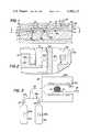
- FIG. 1is a cross-section of a portion of a semiconductor device having a layer of passivating glass and a sealing layer of silicon over the glass in accordance with one embodiment of the invention
- FIG. 2is a plan view of the elements shown in the cross-section of FIG. 1;
- FIG. 3is a schematic diagram of a diffusion furnace in which the sealing layer of silicon is formed on the semiconductor device of FIGS. 1 and 2;
- FIG. 4is a cross-sectional view of another embodiment of the invention in which a second layer of glass is applied over the sealing layer of silicon;
- FIG. 5is a cross-section of a third embodiment of the invention.
- FIG. 1there is shown a cross-section of a portion of a CMOS semiconductor device or integrated circuit 10.
- a circuitis fabricated starting with a body of silicon 11 having a major surface 11a and having a specified concentration of N-type impurities.
- the break shown in the representation of the wafer thicknessis present because the thickness is very large compared to the dimensions of the diffused and deposited regions which constitute the active portion of the circuit.
- the aluminum film 15is divided into many individual traces that interconnect specific regions. For circuit nodes which are to be connected externally, these traces lead to extended metallization areas such as indicated by 15a in FIGS. 1 and 2.
- the aluminumis "sintered” or "alloyed".
- sinteringtakes place ranging from about 400° C. to 500° C. for from about 20 to 40 minutes.
- the ambientis nitrogen or hydrogen or a mixture of nitrogen and hydrogen.
- alloyed regions 16a-cwhere the silicon is not protected by oxide layer 14. It will be understood that higher alloying temperatures much above about 500° C., for example, would result in rapid spreading of the alloyed regions to the point where regions 16a-c would extend completely through the N-regions 13a,b to thereby contact the underlying P-region 12. This would result in an undesirable shorting of the P-N junctions.
- an insulating layeris then deposited over the entire oxide layer 14 and aluminum layer 15 as well as metallized areas 15a.
- a passivating layer of amorphous glass, (SiO 2 )has been used as the insulating layer 17 where the amorphous glass has a phosphorous content, as previously described, in the range of about 3 to 10 percent, as operative limits, and about 5-7 percent preferred limits.
- the glasscannot be deposited at a temperature much above about 500° C. or there results the above described undesirable shorting of the P-N junctions.
- the insulating layeris formed of glass without phosphorous and is also formed of silicon nitride (Si 3 N 4 ).
- Diffusion furnace 30comprises a chamber 30a surrounded by refractory 30b within which thermostatically controlled electric heating coils 30c are embedded.
- the atmosphere within the chamber 30ais supplied with a mixture of silane (SiH 4 ) and nitrogen (N 2 ) gases.
- a tank 25 containing nitrogen 25a and a tank 26 containing 3% silane in nitrogen 26aare attached to a manifold 29 which leads to the furnace chamber 30a.
- the flow rates of the nitrogen and silane as indicated by flow meters 27a, 28aare controlled by valves 27 and 28 respectively and commensurate with the desired deposition rate.
- One or more wafers 10may be supported in an upright position on a quartz or silicon carrier 31 which is inserted into or removed from the furnace by a conventional manually or automatic or machine operated rod 32. Wafer 10 is heated in furnace 30 for the growth of a silicon layer.
- the temperature of furnace 30is in a range of 450° C. to 525° C., approximately, where a temperature of about 475° C. is a preferred temperature.
- the rate of growth of silicon layer 18goes up sharply with temperature and thus for temperatures below about 450° C. in furnace 30 a useful silicon layer may be deposited but the growth process is uneconomically long. For temperatures below about 425° C., from run to run, the silicon in some wafers 10 in some runs does not deposit at all.
- the degree of silicon aluminum alloyingalso increases sharply with temperature.
- the upper limit of the temperature rangeat about 525° C., from run to run, some of the wafers 10 in some runs may have their P-N junction regions near the aluminum-silicon contact points destroyed. Above about 525° C., there is an increase in the destruction of the wafers with temperature in furnace 30.
- depositions of passive sealing silicon layershave been made in the range of 500-1000 A, approximately. This range has been found to be a preferred range of silicon thickness and provides contamination protection with a compromise between a more costly thicker silicon layer while at the thinner limit, a lower device reliability. For silicon layers thinner than 500 A, the saving is only a relatively shorter duration of deposition time. In addition, for these layers thinner than 500 A, during fabrication the plus or minus variation in thickness from run to run may result in some undesirably thin silicon thicknesses on some of the wafers.
- the siliconis formed in the range of 500-3000 A, approximately.
- the silicon filmis desirably not very conductive and provides a high electrical resistivity of approximately 0.25 megohm-centimeter.
- a relatively thin passive silicon layer 18provides a very high resistance but as the film becomes thicker, the resistance decreases. If the silicon layer is of such a thickness that the resistance has substantially decreased, a problem may arise if wire 20 would accidentally touch the silicon layer.
- Examples of silicon layer deposition rates in furnace 30 at temperatures ranging from 450° C. to 525° C. at the indicated silane nitrogen flow rates in a 100 mm. diameter tubeare set forth in the following table.
- a window 19 as shown in FIGS. 1, 2is formed through layers 18 and 17 to allow passage of terminal wire 20 for connecting to node 15a.
- a semiconductor device 10having a silicon layer 18 for protecting the device from contamination from moisture and metallic ions. While device 10 is shown as a portion of a CMOS device, it will be understood that silicon layer 18 may be used in connection with other semiconductor devices requiring such protection from contamination.
- FIG. 4illustrates another embodiment of the invention in a CMOS semiconductor device 10a. All of the fabrication steps up to and including the selective etching of a window in silicon layer 18 and insulating SiO 2 layer 17 are the same as those described previously.
- an additional layer 35 of amorphous glassis deposited over the top of the device such that the edges of this layer at window 19a flow down to coat the sides of the window thus protecting silicon layer 18 from contact with wire 20.
- layer 35must be opened over the aluminum pad to allow wire 20 to be attached.
- the vertical section of layer 35 within window 19amay also be etched away leaving the edges of layers 17, 18 and 35 extending within window 19a.
- layer 35no longer completely protects layer 18 from contact with wire 20.
- FIG. 5illustrates yet another embodiment of the invention in CMOS device 10b. Fabrication of this embodiment is similar to that of the embodiment illustrated in FIGS. 1 and 2. However, in conventional manner, a thin film 36 of nichrome is disposed during the fabrication of the device, as illustrated in FIG. 5, on top of the active silicon regions 11, 12, and 13 prior to the deposition of aluminum layer 15. During the "sintering" or “alloying” process, trimetallic alloy regions 37a-c are formed where the aluminum meets the silicon due to the presence of the nichrome film 36.
- Alloyingcan also be inhibited by depositing aluminum silicon instead of pure aluminum for the interconnects.
- regions 15 in FIG. 1would be of an aluminum silicon composition as deposited.
- the aluminum now being partially saturated with siliconwill not consume as much silicon from the device contact areas when alloyed. This in turn would allow a higher deposition temperature for silicon layer 18.
- window 19bhas been etched wider in area 19c which is defined by silicon layer 18. In this manner, there is substantially decreased any possibility of contact between terminal wire 20 and layer 18.
- passive silicon layer 18can also be deposited by means of evaporation techniques, sputtering techniques and RF plasma methods.
- the waferis maintained at about room temperature or slightly higher and the silicon layer also results in a polycrystalline structure.
- the grain sizecan become so small so as to characterize the polycrystalline structure as amorphous.
Landscapes
- Engineering & Computer Science (AREA)
- Physics & Mathematics (AREA)
- Condensed Matter Physics & Semiconductors (AREA)
- General Physics & Mathematics (AREA)
- Computer Hardware Design (AREA)
- Microelectronics & Electronic Packaging (AREA)
- Power Engineering (AREA)
- Manufacturing & Machinery (AREA)
- Formation Of Insulating Films (AREA)
Abstract
Description
TABLE 1 ______________________________________ Furnace 3% Silane in Nitrogen Rate of Silicon Temperature Nitrogen Rate Rate Layer Growth °C. liter/min. liter/min. A/hr ______________________________________ 450 2.7 6.8 1,600 475 2.7 6.8 5,000 500 2.7 6.8 8,500 525 2.7 6.8 13,000 ______________________________________
Claims (11)
Priority Applications (1)
| Application Number | Priority Date | Filing Date | Title |
|---|---|---|---|
| US06/293,200US4380115A (en) | 1979-12-06 | 1981-08-17 | Method of making a semiconductor device with a seal |
Applications Claiming Priority (2)
| Application Number | Priority Date | Filing Date | Title |
|---|---|---|---|
| US10090579A | 1979-12-06 | 1979-12-06 | |
| US06/293,200US4380115A (en) | 1979-12-06 | 1981-08-17 | Method of making a semiconductor device with a seal |
Related Parent Applications (1)
| Application Number | Title | Priority Date | Filing Date |
|---|---|---|---|
| US10090579ADivision | 1979-12-06 | 1979-12-06 |
Publications (1)
| Publication Number | Publication Date |
|---|---|
| US4380115Atrue US4380115A (en) | 1983-04-19 |
Family
ID=26797678
Family Applications (1)
| Application Number | Title | Priority Date | Filing Date |
|---|---|---|---|
| US06/293,200Expired - Fee RelatedUS4380115A (en) | 1979-12-06 | 1981-08-17 | Method of making a semiconductor device with a seal |
Country Status (1)
| Country | Link |
|---|---|
| US (1) | US4380115A (en) |
Cited By (5)
| Publication number | Priority date | Publication date | Assignee | Title |
|---|---|---|---|---|
| US4680617A (en)* | 1984-05-23 | 1987-07-14 | Ross Milton I | Encapsulated electronic circuit device, and method and apparatus for making same |
| US4872825A (en)* | 1984-05-23 | 1989-10-10 | Ross Milton I | Method and apparatus for making encapsulated electronic circuit devices |
| US4920077A (en)* | 1987-10-09 | 1990-04-24 | Sgs-Thomson Microelectronics S.R.L. | Method of manufacturing monolythic integrated circuits |
| US20070262457A1 (en)* | 1998-12-21 | 2007-11-15 | Mou-Shiung Lin | Top layers of metal for high performance IC's |
| CN110246934A (en)* | 2019-04-28 | 2019-09-17 | 华灿光电(苏州)有限公司 | The production method and light-emitting diode chip for backlight unit of light-emitting diode chip for backlight unit |
Citations (4)
| Publication number | Priority date | Publication date | Assignee | Title |
|---|---|---|---|---|
| US3325586A (en)* | 1963-03-05 | 1967-06-13 | Fairchild Camera Instr Co | Circuit element totally encapsulated in glass |
| US3383568A (en)* | 1965-02-04 | 1968-05-14 | Texas Instruments Inc | Semiconductor device utilizing glass and oxides as an insulator for hermetically sealing the junctions |
| GB1204805A (en)* | 1967-07-07 | 1970-09-09 | Hitachi Ltd | Semiconductor device |
| US3710204A (en)* | 1967-05-20 | 1973-01-09 | Telefunken Patent | A semiconductor device having a screen electrode of intrinsic semiconductor material |
- 1981
- 1981-08-17USUS06/293,200patent/US4380115A/ennot_activeExpired - Fee Related
Patent Citations (4)
| Publication number | Priority date | Publication date | Assignee | Title |
|---|---|---|---|---|
| US3325586A (en)* | 1963-03-05 | 1967-06-13 | Fairchild Camera Instr Co | Circuit element totally encapsulated in glass |
| US3383568A (en)* | 1965-02-04 | 1968-05-14 | Texas Instruments Inc | Semiconductor device utilizing glass and oxides as an insulator for hermetically sealing the junctions |
| US3710204A (en)* | 1967-05-20 | 1973-01-09 | Telefunken Patent | A semiconductor device having a screen electrode of intrinsic semiconductor material |
| GB1204805A (en)* | 1967-07-07 | 1970-09-09 | Hitachi Ltd | Semiconductor device |
Non-Patent Citations (1)
| Title |
|---|
| Abbas et al.; "Doped Polycrystalline Field Shield Process", IBM Tech. Disclosure; vol. 15, No. 6; Nov. 1972.* |
Cited By (16)
| Publication number | Priority date | Publication date | Assignee | Title |
|---|---|---|---|---|
| US4680617A (en)* | 1984-05-23 | 1987-07-14 | Ross Milton I | Encapsulated electronic circuit device, and method and apparatus for making same |
| US4872825A (en)* | 1984-05-23 | 1989-10-10 | Ross Milton I | Method and apparatus for making encapsulated electronic circuit devices |
| US4920077A (en)* | 1987-10-09 | 1990-04-24 | Sgs-Thomson Microelectronics S.R.L. | Method of manufacturing monolythic integrated circuits |
| US20070262457A1 (en)* | 1998-12-21 | 2007-11-15 | Mou-Shiung Lin | Top layers of metal for high performance IC's |
| US20070284750A1 (en)* | 1998-12-21 | 2007-12-13 | Mou-Shiung Lin | Top layers of metal for high performance IC's |
| US20070290348A1 (en)* | 1998-12-21 | 2007-12-20 | Mou-Shiung Lin | Top layers of metal for high performance IC's |
| US20090045516A1 (en)* | 1998-12-21 | 2009-02-19 | Megica Corporation | TOP LAYERS OF METAL FOR HIGH PERFORMANCE IC's |
| US7863654B2 (en) | 1998-12-21 | 2011-01-04 | Megica Corporation | Top layers of metal for high performance IC's |
| US7884479B2 (en) | 1998-12-21 | 2011-02-08 | Megica Corporation | Top layers of metal for high performance IC's |
| US7999384B2 (en) | 1998-12-21 | 2011-08-16 | Megica Corporation | Top layers of metal for high performance IC's |
| US8022545B2 (en) | 1998-12-21 | 2011-09-20 | Megica Corporation | Top layers of metal for high performance IC's |
| US8415800B2 (en) | 1998-12-21 | 2013-04-09 | Megica Corporation | Top layers of metal for high performance IC's |
| US8471384B2 (en) | 1998-12-21 | 2013-06-25 | Megica Corporation | Top layers of metal for high performance IC's |
| US8531038B2 (en) | 1998-12-21 | 2013-09-10 | Megica Corporation | Top layers of metal for high performance IC's |
| CN110246934A (en)* | 2019-04-28 | 2019-09-17 | 华灿光电(苏州)有限公司 | The production method and light-emitting diode chip for backlight unit of light-emitting diode chip for backlight unit |
| CN110246934B (en)* | 2019-04-28 | 2020-04-07 | 华灿光电(苏州)有限公司 | Manufacturing method of light emitting diode chip and light emitting diode chip |
Similar Documents
| Publication | Publication Date | Title |
|---|---|---|
| US4097889A (en) | Combination glass/low temperature deposited Siw Nx Hy O.sub.z | |
| US4134125A (en) | Passivation of metallized semiconductor substrates | |
| US4091407A (en) | Combination glass/low temperature deposited Siw Nx Hy O.sub.z | |
| US3434020A (en) | Ohmic contacts consisting of a first level of molybdenum-gold mixture of gold and vanadium and a second level of molybdenum-gold | |
| CA1271270A (en) | Method of manufacturing a semiconductor device, in which a metallization with a thick connection electrode is provided on a semiconductor body | |
| US3484313A (en) | Method of manufacturing semiconductor devices | |
| US4110125A (en) | Method for fabricating semiconductor devices | |
| JPS62261155A (en) | Manufacture of board device | |
| EP0202240B1 (en) | Coating of iii-v and ii-vi compound semiconductors | |
| US3601888A (en) | Semiconductor fabrication technique and devices formed thereby utilizing a doped metal conductor | |
| JPS6025894B2 (en) | Method for manufacturing semiconductor devices using ion implantation | |
| US3728784A (en) | Fabrication of semiconductor devices | |
| US3837935A (en) | Semiconductor devices and method of manufacturing the same | |
| US3883889A (en) | Silicon-oxygen-nitrogen layers for semiconductor devices | |
| US4380115A (en) | Method of making a semiconductor device with a seal | |
| US5126825A (en) | Wiring structure of a semiconductor device with beta tungsten | |
| US4997794A (en) | Method of making semiconductor device comprising a capacitor and a buried passivation layer | |
| CA1070853A (en) | Seal for a semiconductor device and method therefor | |
| US3979768A (en) | Semiconductor element having surface coating comprising silicon nitride and silicon oxide films | |
| EP0015064B1 (en) | Process for producing bipolar semiconductor device | |
| US3698077A (en) | Method of producing a planar-transistor | |
| WO1993011558A1 (en) | Method of modifying contact resistance in semiconductor devices and articles produced thereby | |
| GB1572819A (en) | Semiconductor device | |
| JPH03191518A (en) | Semiconductor device and manufacture thereof | |
| US3397449A (en) | Making p-nu junction under glass |
Legal Events
| Date | Code | Title | Description |
|---|---|---|---|
| MAFP | Maintenance fee payment | Free format text:PAYMENT OF MAINTENANCE FEE, 4TH YEAR, PL 96-517 (ORIGINAL EVENT CODE: M170); ENTITY STATUS OF PATENT OWNER: LARGE ENTITY Year of fee payment:4 | |
| AS | Assignment | Owner name:SPRAGUE ELECTRIC COMPANY, A MASSACHUSETTS CORP. Free format text:ASSIGNMENT OF ASSIGNORS INTEREST.;ASSIGNOR:SOLID STATE SCIENTIFIC, INC.,;REEL/FRAME:004819/0744 Effective date:19870806 | |
| MAFP | Maintenance fee payment | Free format text:PAYMENT OF MAINTENANCE FEE, 8TH YEAR, PL 96-517 (ORIGINAL EVENT CODE: M171); ENTITY STATUS OF PATENT OWNER: LARGE ENTITY Year of fee payment:8 | |
| AS | Assignment | Owner name:ALLEGRO MICROSYSTEMS, INC., A CORP. OF DE Free format text:ASSIGNMENT OF ASSIGNORS INTEREST;ASSIGNOR:SPRAGUE ELECTRIC COMPANY, A CORP. OF MA;REEL/FRAME:005610/0139 Effective date:19910131 Owner name:ALLEGRO MICROSYSTEMS, INC., A CORP. OF DE Free format text:ASSIGNMENT OF ASSIGNORS INTEREST.;ASSIGNOR:SPRAGUE ELECTRIC COMPANY, A CORP. OF MA;REEL/FRAME:005610/0139 Effective date:19910131 | |
| FEPP | Fee payment procedure | Free format text:MAINTENANCE FEE REMINDER MAILED (ORIGINAL EVENT CODE: REM.); ENTITY STATUS OF PATENT OWNER: LARGE ENTITY | |
| LAPS | Lapse for failure to pay maintenance fees | ||
| FP | Lapsed due to failure to pay maintenance fee | Effective date:19950419 | |
| STCH | Information on status: patent discontinuation | Free format text:PATENT EXPIRED DUE TO NONPAYMENT OF MAINTENANCE FEES UNDER 37 CFR 1.362 |