US4365267A - Passive data monitor for use with polling pattern generator in CATV system - Google Patents
Passive data monitor for use with polling pattern generator in CATV systemDownload PDFInfo
- Publication number
- US4365267A US4365267AUS06/267,508US26750881AUS4365267AUS 4365267 AUS4365267 AUS 4365267AUS 26750881 AUS26750881 AUS 26750881AUS 4365267 AUS4365267 AUS 4365267A
- Authority
- US
- United States
- Prior art keywords
- output
- data
- address
- coupled
- signal
- Prior art date
- Legal status (The legal status is an assumption and is not a legal conclusion. Google has not performed a legal analysis and makes no representation as to the accuracy of the status listed.)
- Expired - Lifetime
Links
- 230000004044responseEffects0.000claimsabstractdescription7
- 238000007493shaping processMethods0.000claimsdescription6
- 238000002955isolationMethods0.000claimsdescription4
- 238000010586diagramMethods0.000description7
- 230000005540biological transmissionEffects0.000description5
- 238000010276constructionMethods0.000description3
- 238000004891communicationMethods0.000description2
- 238000009434installationMethods0.000description2
- 230000002093peripheral effectEffects0.000description2
- 230000008439repair processEffects0.000description2
- 101710186755Putative pterin-4-alpha-carbinolamine dehydratase 1Proteins0.000description1
- 230000008901benefitEffects0.000description1
- 230000002457bidirectional effectEffects0.000description1
- 230000000903blocking effectEffects0.000description1
- 239000003795chemical substances by applicationSubstances0.000description1
- 230000000994depressogenic effectEffects0.000description1
- 238000003780insertionMethods0.000description1
- 230000037431insertionEffects0.000description1
- 230000007257malfunctionEffects0.000description1
- 238000004519manufacturing processMethods0.000description1
- 230000004048modificationEffects0.000description1
- 238000012986modificationMethods0.000description1
- 230000010363phase shiftEffects0.000description1
- 238000012545processingMethods0.000description1
- 230000005236sound signalEffects0.000description1
- 239000000758substrateSubstances0.000description1
- 238000012360testing methodMethods0.000description1
Images


Classifications
- H—ELECTRICITY
- H04—ELECTRIC COMMUNICATION TECHNIQUE
- H04N—PICTORIAL COMMUNICATION, e.g. TELEVISION
- H04N7/00—Television systems
- H04N7/16—Analogue secrecy systems; Analogue subscription systems
- H04N7/173—Analogue secrecy systems; Analogue subscription systems with two-way working, e.g. subscriber sending a programme selection signal
- H04N7/17309—Transmission or handling of upstream communications
- H—ELECTRICITY
- H04—ELECTRIC COMMUNICATION TECHNIQUE
- H04H—BROADCAST COMMUNICATION
- H04H60/00—Arrangements for broadcast applications with a direct linking to broadcast information or broadcast space-time; Broadcast-related systems
- H04H60/09—Arrangements for device control with a direct linkage to broadcast information or to broadcast space-time; Arrangements for control of broadcast-related services
- H04H60/14—Arrangements for conditional access to broadcast information or to broadcast-related services
- H04H60/21—Billing for the use of broadcast information or broadcast-related information
- H—ELECTRICITY
- H04—ELECTRIC COMMUNICATION TECHNIQUE
- H04H—BROADCAST COMMUNICATION
- H04H60/00—Arrangements for broadcast applications with a direct linking to broadcast information or broadcast space-time; Broadcast-related systems
- H04H60/29—Arrangements for monitoring broadcast services or broadcast-related services
- H04H60/32—Arrangements for monitoring conditions of receiving stations, e.g. malfunction or breakdown of receiving stations
- H—ELECTRICITY
- H04—ELECTRIC COMMUNICATION TECHNIQUE
- H04H—BROADCAST COMMUNICATION
- H04H60/00—Arrangements for broadcast applications with a direct linking to broadcast information or broadcast space-time; Broadcast-related systems
- H04H60/35—Arrangements for identifying or recognising characteristics with a direct linkage to broadcast information or to broadcast space-time, e.g. for identifying broadcast stations or for identifying users
- H04H60/38—Arrangements for identifying or recognising characteristics with a direct linkage to broadcast information or to broadcast space-time, e.g. for identifying broadcast stations or for identifying users for identifying broadcast time or space
- H04H60/41—Arrangements for identifying or recognising characteristics with a direct linkage to broadcast information or to broadcast space-time, e.g. for identifying broadcast stations or for identifying users for identifying broadcast time or space for identifying broadcast space, i.e. broadcast channels, broadcast stations or broadcast areas
- H04H60/43—Arrangements for identifying or recognising characteristics with a direct linkage to broadcast information or to broadcast space-time, e.g. for identifying broadcast stations or for identifying users for identifying broadcast time or space for identifying broadcast space, i.e. broadcast channels, broadcast stations or broadcast areas for identifying broadcast channels
- H—ELECTRICITY
- H04—ELECTRIC COMMUNICATION TECHNIQUE
- H04H—BROADCAST COMMUNICATION
- H04H2201/00—Aspects of broadcast communication
- H04H2201/70—Aspects of broadcast communication characterised in that receivers can be addressed
- H—ELECTRICITY
- H04—ELECTRIC COMMUNICATION TECHNIQUE
- H04N—PICTORIAL COMMUNICATION, e.g. TELEVISION
- H04N7/00—Television systems
- H04N7/16—Analogue secrecy systems; Analogue subscription systems
- H04N7/173—Analogue secrecy systems; Analogue subscription systems with two-way working, e.g. subscriber sending a programme selection signal
- H04N2007/17372—Analogue secrecy systems; Analogue subscription systems with two-way working, e.g. subscriber sending a programme selection signal the upstream transmission being initiated or timed by a signal from upstream of the user terminal
Definitions
- the present inventionrelates to a CATV system. More specifically, the invention to a polling signal generator in a CATV system for periodically transmitting a polling signal to terminal units to initiate the transmission of specific data from the terminal units.
- a CATV systemserves to transmit a variety of programs to television sets of terminal units installed in subscriber's homes through coaxial cables.
- Many CATV systemsare capable of performing bidirectional simultaneous communications in addition to program transmission wherein the center simultaneously transmit information to a number of the terminal units and receives information back from them.
- predetermined functions in the terminal unitshave to be periodically or irregularly polled. This polling operation is conducted by transmitting a down data signal to the terminal units, receiving up signals in reply to the down data signal and comparing the command in the down data signal therewith.
- a large-sized computerhas heretofore been necessary. Such a computer cannot easily be transported around the system, as would be desirable.
- a passive data monitor for a CATV systemhaving a single center and a number of terminal units connected to the center for transmitting television programs through cables to the terminal units.
- Each of the terminal unitshas an address setting device capable of arbitrarily setting an address number therein which may be unique to the terminal unit.
- the passive data monitorincludes means for receiving a polling pattern signal having an address code for calling a corresponding terminal unit and a command code for requesting a designated answer from the called terminal unit, and means for comparing an output data signal outputted from the terminal unit in response to the command code with the designated answer requested by the command code and for judging an operational state of the terminal unit from a resultant comparison output.
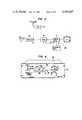
- FIG. 1is an explanatory view showing a CATV system to which the invention is applied;
- FIG. 2is a block diagram showing the installation of a polling pattern generator
- FIG. 3is a block diagram of a passive data monitor of the invention.
- FIG. 4is a front view showing the panel of the passive data monitor
- FIG. 5is a block diagram showing a polling pattern generator of the invention.
- FIG. 6is a front view of the panel of the polling pattern generator of FIG. 5;
- FIG. 7is a plan view showing data switch groups used in the polling pattern generator of FIG. 5;
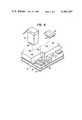
- FIG. 8is a perspective view of a portion of the interior of a terminal unit showing an address block and address setting unit installed in the terminal unit;
- FIG. 9is a structural view showing an alternate installation of the polling pattern generator.
- the CATV systemincludes a single center 1 and terminal units 28 which are provided, for example, in several tens of thousands of subscriber's homes.
- the center 1is connected through coaxial cables to the terminal units 28 in the subscribers' homes 2.
- a main cable 3extends from the center 1 and main cable amplifiers 4 and branching units 5 are provided at predetermined positions on the main cable 3.
- a plurality of branch cables 6extend from each branching unit 5. Extension amplifiers 7 and tap-off units 8 are provided at predetermined points on the branch cables 6.
- Each tap-off unit 8is connected to branch lines 9 which extend to the terminal units 28 in the subscribers' homes 2.
- Each terminal unit 28includes a main unit 10, a television set 11 and a control unit 12.
- the branch line 9is connected to the main unit 10 which is in turn connected to the television set 11 and to the control unit 12.
- the main cable extending from the centeris branched into a first plurality of branch cables which are further branched into a second plurality of branch lines which are finally connected to the terminal units 28.
- a signal receiving antenna 13is installed outside the center 1.
- the antenna 13is connected to a demodulator 15 in a source group 14 in the center 1.
- the source group 14further includes a video disc player 16, a video tape recorder 17 and a studio 18.
- the output signals of the source group 14are applied to a modulation output section 19 composed of two systems.
- One of the two systemsincludes an IF modulator circuit 20, a scramble circuit 21, and an up-converter circuit 22 while the other system includes an IF modulator circuit 23 and an up-converter circuit 34.
- the outputs of the up-converters 22 and 24are connected to the main cable 3 to which a data transceiver 25 is connected for data communication between the center 1 and each main unit 10.
- the data transceiver 25is connected to a computer 26 which is connected to a peripheral unit 27 such as a printer or a display unit.
- the power switch of the television set 11is turned on. With the television set 11 set to a particular unused channel, the control unit 12 is operated so that the frequency of a desired channel to be received is converted into that of the unused channel.
- the channels which can be selected by the control unit 12 as described abovecan be classified into three groups of channels for (A) retransmission programs in which television signals from local station are received without modification, (B) independent programs (free of charge), and (C) chargeable programs. Each group is allocated ten channels, and therefore any of thirty channels can be selected by operating the control unit 12.
- the signals received by the antenna 13are demodulated by the demodulator 15 and then applied to the modulation output section 19.
- the signal thus appliedis modulated by the IF modulator circuit 23.
- the frequency of the signal thus modulatedis increased to a predetermined frequency by the upconverter circuit 24 according to a determined frequency allocation scheme. That is, it is assigned to a predetermined channel.
- the resultant signalis applied through the main cable 3, the branch cable 6, and the branch line 9 to the television sets 11.
- the independent programsinclude weather forecast programs, news programs, and the like.
- the video signalis modulated by the IF modulator circuit 23 and the frequency of the signal thus modulated is increased to that of a predetermined channel by the up-converter circuit 24.
- the resultant signalis applied to the main cable 3. Reception of these programs is free of charge irrespective of the number of times of program reception and the period of time used for program reception. That is, the programs can be received for the basic monthly charge which is paid by the subscriber.
- the chargeable programsinclude new movie programs, special programs, and the like.
- the video signalis modulated by the IF modulator circuit and is then processed by the scrambler circuit 21 so that they cannot be reproduced without special signal processing. Then, the frequency of the signal is increased to that of a predetermined designated channel, and is then applied to the main cable 3.
- the video signalIn order to receive the chargeable programs, the video signal must be descrambled by the main unit 10 in the subscriber's home 2 so that a regular image appears in the television set 11. The subscriber is charged for the reception of the chargeable programs. That is, predetermined charges are summed, and he is requested to pay a special charge at a measured rate in addition to the monthly basic charge.
- the center 1is connected through the coaxial cables to the terminal units in the subscribers' homes 2.
- the data transceiver 25outputs a retrieving signal at predetermined time intervals so that the terminal units 28 are called with their assigned address numbers. That is, the channels received by the terminal units at the time of transmission of the retrieving signal are detected, this operation being referred to as "polling".
- each terminal unit 28answers the data transceiver 25 with data representative of the channel which was received by the terminal unit at the time of polling.
- reception and transmission data for the data transceiver 25are arranged and stored by the computer 26 and are displayed or printed out by the peripheral unit 27.
- the polling operationis carried out at predetermined time intervals of several seconds to several tens of second and therefore audience ratings can be readily calculated.
- the subscribersmay participate in the production of programs.
- theyby operating the control units 12, they can answer to the programs while watching the television sets 11.
- the answersare transmitted through the coaxial cables to the center 1.
- FIG. 2shows in block diagram form a preferred embodiment of a polling pattern generator of the invention.
- a trap 30 for blocking the down data signal but which passes the video signalhas an input connected to a branch line 9.
- a passive data monitor 32hereinafter abbreviated to "PDM”.
- the output of the PDM 32is connected to a main unit 10.
- An address setting unit 33which will be hereinafter described in greater detail, is detachably provided at the main unit 10, and is connected through a cable to the PDM 32.
- Reference numeral 34indicates a polling pattern generator, hereinafter abbreviated to "PPG".
- the output of the PPG 34is connected to the mixer 31.
- the PPG 34produces a polling down data signal either by itself or in response to an external data unit coupled in at an external data input terminal.
- the PPG 34can thus poll the respective terminal units 28 through the connection provided between the branch line 9 and the main unit 10 in FIG. 1.
- a down data signalwhich will hereinafter be termed an "FSK signal” as it is a frequency shift keyed signal, and video signals and the like are transmitted from the center 1 and are received at the trap 30. Only the video signals are transmitted through the trap 30, the PDM 32 and the main unit 10 to television sets 11. In this manner, the television set 11 can reproduce the video and audio signals in the ordinary manner even during polling.
- FSK signalfrequency shift keyed signal
- the PPG 34normally generates a polling pattern signal having in combination an address code and a command code in the same transmission mode as used by the center 1.
- the polling signalsincorporate all command codes in combination with respective address data which are repeatedly transmitted in sequence from the polling generator.
- the polling signalsare transmitted through the mixer 31 to the PDM 32.
- the terminal unit 28is set to select an address corresponding to a special command code. In this manner, the PDM 32 can determine the content of an answer from the terminal unit 28.
- the address for the PDM 32can be freely selected and set by the address setting unit 33 in the main unit 10. The construction and operation of the address setting unit 33 will be hereinafter described in greater detail.
- the main unit 10receives only the polling pattern of the address code code set by the address setting unit 33 of the polling patterns from the PPG 34 and outputs an answer corresponding to the command code followed by the address code to the PDM 32.
- the PDM 32compares the address code thus set with an answer signal from the main unit 10 and thus determines whether a normal operation or an erroneous operation has taken place according to whether or not the received address code agrees with the command code.
- FIG. 3is a block diagram of the PDM 32.
- the PDM 32has an input terminal 35 connected to the mixer, an output terminal 36 connected to the main unit 10, and an address output terminal 37 connected to the address setting unit 33.
- the output terminal of a signal splitter 38is connected to the output terminal 36 while the high side terminal thereof is connected to the input terminal 35 and the low side terminal to a bandpass filter 39.
- the output of the bandpass filter 39is connected to a signal detector 40.
- the output of the signal detector 40is connected to inputs of both a high-pass filter 41 and a low-pass filter 42.
- the output of the high-pass filter 41is connected through a wave shaping circuit 43 to a clock generator 44.
- a BPS-to-NRZ code converter circuit 45receives the output of the wave shaping circuit 43 and the output of the clock generator 44 converting the BPS code into the NRZ code.
- a serial-to-parallel converter circuit 46converts the output of the converter circuit 45 to a parallel signal.
- the output of the low-pass filter 42is connected to a latch control circuit 47.
- the output of the latch control circuit 47is connected to both a data latch circuit 48 and a comparator 49.
- the output of the converter circuit 46is connected to the data latch circuit 48.
- the output of the data latch circuit 48is connected to both the comparator 49 and a monitor circuit 50.
- the output of the comparator 49is connected to a display unit 41, which may be an LED device or the like.
- Reference numeral 52depicts a selector circuit which can be set manually.
- the output of the selector circuit 52is connected to the inputs of both a data ROM 53 and an address ROM 54 which store predetermined data and addresses, respectively.
- the output of the data ROM 53is connected to the comparator 49.
- the ouput of the address ROM 54is connected through an isolation buffer circuit 55 to the address output terminal 37.
- the address setting unit 33is connected to the address output terminal 37.
- FIG. 4shows a front panel of the PDM 32.
- the front panelhas connectors 57 and 58 for the input terminal 35 and the output terminal 36, respectively, on the upper leftside portion, a multiple pin connector 59 for the address output terminal 37 below the connector 58, and LEDs (light emission diodes) 60 through 65 as the monitor circuit 50 and the display unit 51 in the vicinity of the central portion.
- the LEDs 60 to 62 for the monitor circuitare aligned rectilinearly horizontally.
- the characters A through J placed above the LEDs 60indicate answer data from the terminal units.
- the character above the LED 61corresponds to a parity bit.
- AD designated above the LED 62indicates an additional bit.
- the LEDs 63 through 65 for displaying the terminal units conditionare arranged above the LEDs 60 through 62.
- the LED 63 identified by the characters RCPindicates that an up signal, hereinafter abbreviated as "PSK” as it is phase shift keyed signal, from the main unit 10 has been received.
- the LED 64identified with the characters GOOD, indicates that the PSK signal is normal.
- the LED 65 labeled NGindicates that the PSK signal is in error.
- the panel 56also incorporates a power switch 66 and a power lamp 67 for indicating the on or off state of the power switch 66 on the upper rightside portion.
- the panelalso has a check number knob 68, which is coupled to a rotary switch, positioned under the power switch 66. This rotary switch is used in the selector circuit 52.
- FIG. 5is a block diagram showing the circuit arrangement of the aforementioned PPG 34.
- the outputs of a data ROM 70 in which is stored a variety of address codes and command codes and outputs of a data switch 71 which is used to set the address code and the command code manuallyare connected to a selector circuit 72.
- a control signal from a timing control circuit 73 which determines the timing for producing datais connected to both the data ROM 70 and the data switch 71.
- the output of the selector circuit 72is connected to an NRZ-to-BPS code converter circuit 74 for converting the NRZ code to the BPS code.
- the output of the converter circuit 74is connected to an FSK signal transmitter circuit 75.
- the output of the transmitter circuit 75is connected to an FSK output terminal 76.
- An external data input terminal 77 for inputting data from an external deviceis connected directly to the converter circuit 74.
- FIG. 6shows the outer appearance of the PPG 34.
- a panel 78 at the front of this unithas a power switch 79 and a power lamp 80 for indicating the on or off state of the power switch 79 on the upper left portion thereof, connectors 81 and 82 forming respectively the external input terminal 77 and the output terminal 76, below the power switch 79, and a switch 83 for selecting one of the external input data and the internal data located on the right of the panel.
- the panel 78also incorporates attenuation switches 84 for setting output signal levels aligned in a row horizontally on the central portion. These attenuation switches 84 are a push-button type and are used for determining the output signal level.
- the panelalso has a polling lamp 85 for indicating polling and a function knob 86 for varying the polling speed on the right side.
- the PPG 35incorporates a detachable cover 87 on the upper central portion and switch groups for setting desired data under the cover 87.
- FIG. 7shows the construction of the switch groups to which access is made by opening the cover 87 of the PPG 34.
- the switch groupscorrespond to the aforementioned data switch 71.
- the individual switches of the four switch groups 88, 89, 90 and 91can set to either "H" or "L" corresponding to high and low logic levels.
- the switches 88 and 90have six individual switches corresponding to six digits while the switch groups 89 and 90 have five switches corresponding to five digits.
- the switch groups 88 and 89are used to set a group address and the switch 90 is used to set an individual address.
- the switch 91is used to set a command.
- FIG. 8shows the address setting section in the main unit 10 with the cover of the main unit 10 removed.
- a printed circuit board 93is secured in an insulating manner onto a metallic substrate 92.
- An address socket 94 for determining the address of the main unit 10is mounted at the corner of the printed circuit board 93.
- the address socket 94incorporates two rows of twelve socket holes 95 opening upwardly in two rows and aligned linearly.
- an address block 96 for setting the address of the main unit 10is engaged with the address socket 94.
- This address block 96which is formed of plastic or the like, has two rows of twelve pins 97 on the lower surface. By selectively making connection between designated ones of the pins 97 inside the address block 96, a desired address is determined.
- the pins 97are inserted into the socket holes 95.
- the address block 96is pulled out of the address socekt 74 and the address setting unit 33 is instead engaged with the address socket 94.
- Pins 98project from the lower portion of the address setting unit 33.
- the address setting unit 33is electrically connected to the address socket 94.
- the control signal from the PDM 32connects any of the pins 98 by a switching circuit built in the address setting unit 33 wherein the address is freely settable.
- the power switch 79When the power switch 79 is turned on, the power lamp 80 is lit, and power is coupled to the various operating circuits. If it is desired to use the built-in data ROM 70 or the data switch 71, the selector switch 83 is set to the "INT" position. To set the output signal level, the attenuation switches 84 are set so as to produce the desired level. For example, if an output signal level of -38 dB is desired, the push-button 20, 10, 5 and 3 of the attenuation switches 84 are depressed.
- the power switch 79When the power switch 79 is turned on as described above, the address code and the data code are sequentially produced periodically with predetermined period at the connector 82. Then, the polling operation is conducted. When this type of data is outputted, the polling lamp 85 is turned on. The polling speed (or period) can be varied by turning the function knob 86 (see FIG. 6).
- the timing control circuit 73When the power is on as described above, the timing control circuit 73 periodically outputs a timing pulse in a predetermined period to the data ROM 70.
- the data ROM 70thus applies the data stored therein at every timing pulse to the selector circuit 72.
- the selector circuit 72operates to cut off the inputting of the switch data 71 and to apply only the input from the data ROM 70 to the converter circuit 74 which converts the NRZ code from the data ROM 76 to BPS code.
- the data thus convertedis modulated with a predetermined frequency by the FSK signal transmitter circuit 75 and amplified.
- the data signal thus modulated and amplifiedis applied from the output terminal 76 and through the connector 82.
- the data ROM 70is stored a plurality of sets of combinations of an address code and a command code.
- the sets of dataare sequentially outputted, one set at every timing pulse.
- the datais repeatedly outputted starting from the initial data. Specific examples of the types of the data will be described. (The data ROM 70 is a 256 ⁇ 8 bit type.)
- the data of the address code and the command codeare sequentially read out from the data ROM 70.
- the datacontains steps sequentially numbered “00" to “29” steps. When step “29" of the data and this operation is repeated.
- the interval of generating the timing pulses from the timing control circuit 73is varied by operating the function knob 86, the polling speed or period varies.
- the built-in switch groups 88 through 91are accessible. With the cover 87 thus removed, the selector circuit 72 is simultaneously automatically selected and only the signal of the data switch 71 is applied to the converter circuit 74.
- the switches 88 through 91can be manually set to the "H” or "L” position and the switches 88 and 89 are used to freely select the group address code, the switch 90 to set the individual code and the switch 91 to freely set the command code. (The start, index and parity codes are separately set beforehand.)
- the data thus setis applied to the selector circuit 72 using the timing pulse signal from the timing control circuit 73 as described above.
- the output of the generator for generating other datais connected to the connector 81.
- the selector switch 83is set to the "EXT" position.
- the external data inputis applied directly to the converter circuit 74.
- the external data thus appliedis outputted through the transmitter circuit.
- the switch 66When the switch 66 is turned on, the power lamp 67 is lit and power is supplied to the various circuits of the units.
- the check number knob 68When the check number knob 68 is turned, the built-in ROM 53 and ROM 54 are selected and the stored polling list is changed.
- a pin plug(not shown) is connected to the address setting unit 33 by insertion thereof into the pin socket 59.
- the address of the mode selected by the check number knob 68is outputted as a control signal from the pin socket 59.
- the PSK signal from the main unit 10is applied to the connector 57. When the PSK signal is thus applied, the RCP LED 63 is lit indicating the reception of the PSK signal.
- the LED 64 corresponding to GOODis lit while if the PSK signal is in error, the LED 65 corresponding to NG is lit.
- the LED 60indicates the content of the PSK signal, the LED 61 indicates the presence or absence of parity, and the LED 62 indicates the presence or absence of the additional bit (see FIG. 4).
- the selector circuit 52When the selector circuit 52, which is set by the check number knob 68, is operated, the selector circuit 52 selects the address number corresponding to the function to be checked to thereby output the desired address number from the address ROM 54 to the isolation buffer circuit 55 and to apply the address signal to the address output terminal 37.
- the address setting unit 33With the address setting unit 33 connected through a coaxial cable to the address output terminal 37 (the pin connector 59), the address signal is applied to the address setting unit 33.
- the address setting unit 33sets interconnections between ones of the pins 98 (FIG. 8).
- the pins 98 of the address setting unit 33are inserted into the pin holes 95 of the address block 94, the address is set in the main unit 10 through the pin 98.
- the set address numberis polled, the data is applied to the main unit 10.
- the selected signalis simultaneously applied to the data ROM 53.
- the data corresponding to the address numberis applied from the data ROM 53 to the comparator 49. That is, the address number and the data are treated as a pair.
- the special address numberis always simultaneously outputted in combination with the special data.
- the address number and the content of the dataare equal to the address number and the answer data corresponding to the following command data generated by the PPG 34.
- a commandis applied, as shown in FIG. 2, from the PPG 34 through the PDM 32 to the main unit 10.
- This commandcontains an address number and data in combination as described above.
- a plurality of types of the commandsare sequentially outputted.
- the initial commandis again outputted starting from the first command. More particularly, several types of commands are continuously and repeatedly sequentially outputted from the PPG 34. Since the address number is set to a special value by the address setting unit 33 as described above, the main unit 10 starts operation upon reception of a particular one of the addresses applied from the PPG 34, reads the data followed by the address number and transmits an answering PSK signal toward the center 1 and accordingly toward the PDM 32.
- the PSK signalis applied from the input terminal 36 (the connector 58) to the signal splitter 38 and from these applied to the bandpass filter 39.
- the FSK signalcorresponds to the high frequency and the PSK signal to the low frequency.
- the PSK signalafter passing through the bandpass filter 39 is detected by the signal detector 40, and is then applied to both the high-pass filter 41 and the low-pass filter 42.
- the output signal from the high-pass filter 41is applied to both the wave shaping circuit 43 and the clock generator 44.
- the converter circuit 45converts the BPS code into the NRZ code and to apply the NRZ code to the serial-to-parallel converter circuit 45.
- the PSK signalis applied to the clock generator 44 which detects and outputs only the clock information in the signal.
- the clock generator 44thus applies the clock signal thus produced to both the converter circuit 45 which uses the clock signals to time their operations. With the clock signal thus applied to the converter circuit 45, the PSK signal is applied to the converter circuit 46 at every clock pulse.
- the data latch circuit 48receives the signal from the converter circuit 46 and holds the PSK signal of a predetermined bit-number parallel signal (for example, eight-bit parallel signal).
- the output of the data latch circuit 48is displayed by the monitor circuit 50.
- the latch control circuitdetects effective sections of the data and thus to control the data rewriting operation in the latch circuit.
- the output of the data latch circuit 48is applied to the comparator 49.
- the comparator 49receives the preset data from the data ROM 53, compares the output from the data latch circuit 48 with the preset data from the data ROM 53, and applies the compared result output to the display unit 51. If the two signals are the same, it is indicated that the main unit 10 is operating normally by lighting the GOOD LED 64. If, however, the two signals are different, it is indicated that the main unit 10 is operating erroneously by lighting the NG LED 65.
- FIG. 9is a block diagram showing a system in which the functions of the terminal units 28 can be tested by the center 1 and the PDM 32.
- the center 1incorporates a polling pattern generator circuit 100 connected to a main cable 3.
- the generator circuit 100stores a plurality of address numbers and a plurality of data for checking the operating state of the terminal units 28 corresponding to the address numbers.
- the data corresponding to the address numbersis periodically applied to the main cable 3.
- the polling pattern signalsare fed during an idling time for polling. (This time has a duration of 5 to 10 seconds.)
- the address in the polling pattern signalis not the one used in the address of a plurality of terminal units 28, but is a special address not actually used so that a malfunction does not occur.
- the PDM 32is connected to the branch lines 9 from by the main cable 3.
- the main unit 10is connected to the output of the PDM 32.
- An address setting unit 33is connected to the PDM 32 as described above.
- the address setting unit 33is connected to the address socket of the main unit 10. Since in this embodiment the center 1 periodically outputs the checking address and the data during the idling time of polling, when the address to be checked by the PDM 32 is set, the address setting unit 33 defines the address number of the main unit 10.
- the main unit 10When the set address polling pattern signal is transmitted to the main unit 10, the main unit 10 outputs a PSK signal corresponding to the data to the PDM 32 and the PDM 32 analyzes the PSK signal in the same manner as described above.
- the polling pattern generator described abovethe polling pattern is generated using a simple circuit arrangement and without using a large-size computer. Moreover, since the generator of the invention is portable, it can be operated in the vicinity of the terminal units without moving the terminal unit as well as being used to test and repair terminal units in a factory or repair facility.
Landscapes
- Engineering & Computer Science (AREA)
- Signal Processing (AREA)
- Multimedia (AREA)
- Small-Scale Networks (AREA)
- Testing, Inspecting, Measuring Of Stereoscopic Televisions And Televisions (AREA)
- Monitoring And Testing Of Transmission In General (AREA)
Abstract
Description
TABLE 1 ______________________________________ D.sub.8 D.sub.7 D.sub.6 D.sub.5 D.sub.4 D.sub.3 D.sub.2 D.sub.1 ______________________________________ 0 0 0 0 0 0 0 0 0 0 0 1 0 0 0 0 0 0 0 0 Spare 0 2 0 0 0 0 0 0 0 0 0 3 0 0 0 0 0 0 0 0 -- Frame 0 4 1 1 1 1 1 1 1 1 MG.sub.1 0 5 1 1 1 1 0 0 1 0 0 6 0 0 0 0 0 0 0 0 0 7 1 0 0 1 1 1 1 1 MP.sub.1 4E 0 8 1 1 1 1 1 0 0 0 0 9 0 0 0 0 0 0 0 0 0 A 1 0 1 0 1 1 1 1 MP.sub.2 MLON 0 B 1 0 0 0 0 1 1 0 0 C 0 0 0 0 0 0 0 0 0 D 1 0 1 1 0 1 1 1 MP.sub.3 PPO 0 E 1 0 0 1 0 1 0 0 0 F 0 0 0 0 0 0 0 0 1 0 1 0 1 1 1 0 1 1 MP.sub.4 PCD 1 1 1 1 1 0 0 1 1 0 1 2 0 0 0 0 0 0 0 0 1 3 1 0 1 1 1 1 0 1 MP.sub.5 4E 1 4 1 1 1 1 1 0 0 0 ______________________________________
TABLE 2 ______________________________________ D.sub.8 D.sub.7 D.sub.6 D.sub.5 D.sub.4 D.sub.3 D.sub.2 D.sub.1 ______________________________________ 1 5 0 0 0 0 0 0 0 0 1 6 1 0 1 1 1 1 1 0 MP.sub.6 MLOFF 1 7 1 1 0 0 0 1 0 0 1 8 0 0 0 0 0 0 0 0 1 9 1 0 0 1 1 1 1 0 MP.sub.7 0010 1 A 1 0 1 1 0 0 1 0 1 B 0 0 0 0 0 0 0 0 1 C 1 0 1 0 1 1 1 0 MP.sub.8 4E 1 D 1 1 1 1 1 0 1 0 1 E 0 0 0 0 0 0 0 0 1 F 1 0 1 1 0 1 1 0 MP.sub.9 4-0 2 0 1 0 0 0 0 0 1 0 2 1 0 0 0 0 0 0 0 0 2 2 1 0 1 1 0 1 1 0 MP.sub.9 MLOFF 2 3 1 1 0 0 0 1 1 0 2 4 0 0 0 0 0 0 0 0 2 5 1 0 1 1 0 1 1 0 MP.sub.9 DC 2 6 1 1 0 1 0 1 0 0 2 7 0 0 0 0 0 0 0 0 2 8 1 1 0 0 0 0 0 0 AG 2 9 1 0 0 0 0 0 0 0 ______________________________________
Claims (4)
Applications Claiming Priority (2)
| Application Number | Priority Date | Filing Date | Title |
|---|---|---|---|
| JP7358480AJPS56169481A (en) | 1980-05-30 | 1980-05-30 | Inspection signal analyzer in catv system |
| JP55-73584 | 1980-05-30 |
Publications (1)
| Publication Number | Publication Date |
|---|---|
| US4365267Atrue US4365267A (en) | 1982-12-21 |
Family
ID=13522494
Family Applications (1)
| Application Number | Title | Priority Date | Filing Date |
|---|---|---|---|
| US06/267,508Expired - LifetimeUS4365267A (en) | 1980-05-30 | 1981-05-27 | Passive data monitor for use with polling pattern generator in CATV system |
Country Status (3)
| Country | Link |
|---|---|
| US (1) | US4365267A (en) |
| JP (1) | JPS56169481A (en) |
| CA (1) | CA1161544A (en) |
Cited By (13)
| Publication number | Priority date | Publication date | Assignee | Title |
|---|---|---|---|---|
| US4450481A (en)* | 1981-08-25 | 1984-05-22 | E-Com Corporation | Tamper-resistant, expandable communications system |
| US4475121A (en)* | 1980-05-30 | 1984-10-02 | Pioneer Electronic Corporation | Polling pattern generator for CATV system |
| US4994908A (en)* | 1988-12-23 | 1991-02-19 | Scientific-Atlanta, Inc. | Interactive room status/time information system |
| US5053883A (en)* | 1988-12-23 | 1991-10-01 | Scientific-Atlanta, Inc. | Terminal polling method |
| US5093786A (en)* | 1989-01-27 | 1992-03-03 | Fleetwood Furniture Company, Inc. | Remote response system |
| US5130983A (en)* | 1990-03-27 | 1992-07-14 | Heffner Iii Horace W | Method of polling to determine service needs and the like |
| US5724357A (en)* | 1992-01-28 | 1998-03-03 | Fleetwood Group, Inc. | Remote response system and data transfer protocol |
| US5887243A (en) | 1981-11-03 | 1999-03-23 | Personalized Media Communications, L.L.C. | Signal processing apparatus and methods |
| US6021119A (en)* | 1994-06-24 | 2000-02-01 | Fleetwood Group, Inc. | Multiple site interactive response system |
| US20020002709A1 (en)* | 2000-03-28 | 2002-01-03 | Young-Sang An | Method and system for transmitting multimedia data with downstream data transfer over local TV broadcasting channel and for receiving request with upstream data transfer over another channel |
| US20100023316A1 (en)* | 2002-08-15 | 2010-01-28 | Anthony Knowles | Participant response system and method |
| US7769344B1 (en) | 1981-11-03 | 2010-08-03 | Personalized Media Communications, Llc | Signal processing apparatus and methods |
| USRE47642E1 (en) | 1981-11-03 | 2019-10-08 | Personalized Media Communications LLC | Signal processing apparatus and methods |
Citations (4)
| Publication number | Priority date | Publication date | Assignee | Title |
|---|---|---|---|---|
| US3997718A (en)* | 1973-02-01 | 1976-12-14 | The Magnavox Company | Premium interactive communication system |
| US4058829A (en)* | 1976-08-13 | 1977-11-15 | Control Data Corporation | TV monitor |
| US4107734A (en)* | 1977-01-31 | 1978-08-15 | R. D. Percy & Company | Television viewer reaction determining system |
| US4245245A (en)* | 1975-02-24 | 1981-01-13 | Pioneer Electronic Corporation | Interactive CATV system |
- 1980
- 1980-05-30JPJP7358480Apatent/JPS56169481A/enactivePending
- 1981
- 1981-05-27CACA000378441Apatent/CA1161544A/ennot_activeExpired
- 1981-05-27USUS06/267,508patent/US4365267A/ennot_activeExpired - Lifetime
Patent Citations (4)
| Publication number | Priority date | Publication date | Assignee | Title |
|---|---|---|---|---|
| US3997718A (en)* | 1973-02-01 | 1976-12-14 | The Magnavox Company | Premium interactive communication system |
| US4245245A (en)* | 1975-02-24 | 1981-01-13 | Pioneer Electronic Corporation | Interactive CATV system |
| US4058829A (en)* | 1976-08-13 | 1977-11-15 | Control Data Corporation | TV monitor |
| US4107734A (en)* | 1977-01-31 | 1978-08-15 | R. D. Percy & Company | Television viewer reaction determining system |
Cited By (118)
| Publication number | Priority date | Publication date | Assignee | Title |
|---|---|---|---|---|
| US4475121A (en)* | 1980-05-30 | 1984-10-02 | Pioneer Electronic Corporation | Polling pattern generator for CATV system |
| US4450481A (en)* | 1981-08-25 | 1984-05-22 | E-Com Corporation | Tamper-resistant, expandable communications system |
| US9043859B1 (en) | 1981-11-02 | 2015-05-26 | Personalized Media Communications, Llc | Signal processing apparatus and methods |
| US7908638B1 (en) | 1981-11-03 | 2011-03-15 | Personalized Media Communications LLC | Signal processing apparatus and methods |
| US8683539B1 (en) | 1981-11-03 | 2014-03-25 | Personalized Media Communications, Llc | Signal processing apparatus and methods |
| USRE48682E1 (en) | 1981-11-03 | 2021-08-10 | Personalized Media Communications LLC | Providing subscriber specific content in a network |
| USRE48633E1 (en) | 1981-11-03 | 2021-07-06 | Personalized Media Communications LLC | Reprogramming of a programmable device of a specific version |
| USRE48565E1 (en) | 1981-11-03 | 2021-05-18 | Personalized Media Communications LLC | Providing a subscriber specific solution in a computer network |
| US5887243A (en) | 1981-11-03 | 1999-03-23 | Personalized Media Communications, L.L.C. | Signal processing apparatus and methods |
| USRE48484E1 (en) | 1981-11-03 | 2021-03-23 | Personalized Media Communications, Llc | Signal processing apparatus and methods |
| US10715835B1 (en) | 1981-11-03 | 2020-07-14 | John Christopher Harvey | Signal processing apparatus and methods |
| USRE47968E1 (en) | 1981-11-03 | 2020-04-28 | Personalized Media Communications LLC | Signal processing apparatus and methods |
| US7734251B1 (en) | 1981-11-03 | 2010-06-08 | Personalized Media Communications, Llc | Signal processing apparatus and methods |
| US7747217B1 (en) | 1981-11-03 | 2010-06-29 | Personalized Media Communications, Llc | Signal processing apparatus and methods |
| US7752649B1 (en) | 1981-11-03 | 2010-07-06 | Personalized Media Communications, Llc | Signal processing apparatus and methods |
| US7752650B1 (en) | 1981-11-03 | 2010-07-06 | Personalized Media Communications, Llc | Signal processing apparatus and methods |
| US7761890B1 (en) | 1981-11-03 | 2010-07-20 | Personalized Media Communications, Llc | Signal processing apparatus and methods |
| US7764685B1 (en) | 1981-11-03 | 2010-07-27 | Personalized Media Communications, L.L.C. | Signal processing apparatus and methods |
| US7769170B1 (en) | 1981-11-03 | 2010-08-03 | Personalized Media Communications, Llc | Signal processing apparatus and methods |
| US7769344B1 (en) | 1981-11-03 | 2010-08-03 | Personalized Media Communications, Llc | Signal processing apparatus and methods |
| US7774809B1 (en) | 1981-11-03 | 2010-08-10 | Personalized Media Communications, Llc | Signal processing apparatus and method |
| US7784082B1 (en) | 1981-11-03 | 2010-08-24 | Personalized Media Communications, Llc | Signal processing apparatus and methods |
| US7783252B1 (en) | 1981-11-03 | 2010-08-24 | Personalized Media Communications, Llc | Signal processing apparatus and methods |
| US7793332B1 (en) | 1981-11-03 | 2010-09-07 | Personalized Media Communications, Llc | Signal processing apparatus and methods |
| US7797717B1 (en) | 1981-11-03 | 2010-09-14 | Personalized Media Communications, Llc | Signal processing apparatus and methods |
| US7801304B1 (en) | 1981-11-03 | 2010-09-21 | Personalized Media Communications, Llc | Signal processing apparatus and methods |
| US7805738B1 (en) | 1981-11-03 | 2010-09-28 | Personalized Media Communications, Llc | Signal processing apparatus and methods |
| US7805749B1 (en) | 1981-11-03 | 2010-09-28 | Personalized Media Communications, Llc | Signal processing apparatus and methods |
| US7805748B1 (en) | 1981-11-03 | 2010-09-28 | Personalized Media Communications, Llc | Signal processing apparatus and methods |
| US7810115B1 (en) | 1981-11-03 | 2010-10-05 | Personalized Media Communications, Llc | Signal processing apparatus and methods |
| US7814526B1 (en) | 1981-11-03 | 2010-10-12 | Personalized Media Communications, Llc | Signal processing apparatus and methods |
| US7817208B1 (en) | 1981-11-03 | 2010-10-19 | Personalized Media Communications, Llc | Signal processing apparatus and methods |
| US7818776B1 (en) | 1981-11-03 | 2010-10-19 | Personalized Media Communications, Llc | Signal processing apparatus and methods |
| US7818761B1 (en) | 1981-11-03 | 2010-10-19 | Personalized Media Communications, Llc | Signal processing apparatus and methods |
| US7818777B1 (en) | 1981-11-03 | 2010-10-19 | Personalized Media Communications, Llc | Signal processing apparatus and methods |
| US7818778B1 (en) | 1981-11-03 | 2010-10-19 | Personalized Media Communications, Llc | Signal processing apparatus and methods |
| US7823175B1 (en) | 1981-11-03 | 2010-10-26 | Personalized Media Communications LLC | Signal processing apparatus and methods |
| US7827587B1 (en) | 1981-11-03 | 2010-11-02 | Personalized Media Communications, Llc | Signal processing apparatus and methods |
| US7827586B1 (en) | 1981-11-03 | 2010-11-02 | Personalized Media Communications, Llc | Signal processing apparatus and methods |
| US7831204B1 (en) | 1981-11-03 | 2010-11-09 | Personalized Media Communications, Llc | Signal processing apparatus and methods |
| US7830925B1 (en) | 1981-11-03 | 2010-11-09 | Personalized Media Communications, Llc | Signal processing apparatus and methods |
| US7836480B1 (en) | 1981-11-03 | 2010-11-16 | Personalized Media Communications, Llc | Signal processing apparatus and methods |
| US7840976B1 (en) | 1981-11-03 | 2010-11-23 | Personalized Media Communications, Llc | Signal processing apparatus and methods |
| US7844995B1 (en) | 1981-11-03 | 2010-11-30 | Personalized Media Communications, Llc | Signal processing apparatus and methods |
| US7849493B1 (en) | 1981-11-03 | 2010-12-07 | Personalized Media Communications, Llc | Signal processing apparatus and methods |
| US7849479B1 (en) | 1981-11-03 | 2010-12-07 | Personalized Media Communications, Llc | Signal processing apparatus and methods |
| US7849480B1 (en) | 1981-11-03 | 2010-12-07 | Personalized Media Communications LLC | Signal processing apparatus and methods |
| US7856650B1 (en) | 1981-11-03 | 2010-12-21 | Personalized Media Communications, Llc | Signal processing apparatus and methods |
| US7856649B1 (en) | 1981-11-03 | 2010-12-21 | Personalized Media Communications, Llc | Signal processing apparatus and methods |
| US7860249B1 (en) | 1981-11-03 | 2010-12-28 | Personalized Media Communications LLC | Signal processing apparatus and methods |
| US7860131B1 (en) | 1981-11-03 | 2010-12-28 | Personalized Media Communications, Llc | Signal processing apparatus and methods |
| US7861278B1 (en) | 1981-11-03 | 2010-12-28 | Personalized Media Communications, Llc | Signal processing apparatus and methods |
| US7861263B1 (en) | 1981-11-03 | 2010-12-28 | Personalized Media Communications, Llc | Signal processing apparatus and methods |
| US7864248B1 (en) | 1981-11-03 | 2011-01-04 | Personalized Media Communications, Llc | Signal processing apparatus and methods |
| US7865920B1 (en) | 1981-11-03 | 2011-01-04 | Personalized Media Communications LLC | Signal processing apparatus and methods |
| US7864956B1 (en) | 1981-11-03 | 2011-01-04 | Personalized Media Communications, Llc | Signal processing apparatus and methods |
| US7870581B1 (en) | 1981-11-03 | 2011-01-11 | Personalized Media Communications, Llc | Signal processing apparatus and methods |
| US7889865B1 (en) | 1981-11-03 | 2011-02-15 | Personalized Media Communications, L.L.C. | Signal processing apparatus and methods |
| US10616638B1 (en) | 1981-11-03 | 2020-04-07 | Personalized Media Communications LLC | Signal processing apparatus and methods |
| US10609425B1 (en) | 1981-11-03 | 2020-03-31 | Personalized Media Communications, L.L.C. | Signal processing apparatus and methods |
| US8601528B1 (en) | 1981-11-03 | 2013-12-03 | Personalized Media Communications, L.L.C. | Signal processing apparatus and methods |
| USRE47867E1 (en) | 1981-11-03 | 2020-02-18 | Personalized Media Communications LLC | Signal processing apparatus and methods |
| US10523350B1 (en) | 1981-11-03 | 2019-12-31 | Personalized Media Communications LLC | Signal processing apparatus and methods |
| USRE47642E1 (en) | 1981-11-03 | 2019-10-08 | Personalized Media Communications LLC | Signal processing apparatus and methods |
| US7992169B1 (en) | 1981-11-03 | 2011-08-02 | Personalized Media Communications LLC | Signal processing apparatus and methods |
| US8046791B1 (en) | 1981-11-03 | 2011-10-25 | Personalized Media Communications, Llc | Signal processing apparatus and methods |
| US8060903B1 (en) | 1981-11-03 | 2011-11-15 | Personalized Media PMC Communications, L.L.C. | Signal processing apparatus and methods |
| US8112782B1 (en) | 1981-11-03 | 2012-02-07 | Personalized Media Communications, Llc | Signal processing apparatus and methods |
| US8191091B1 (en) | 1981-11-03 | 2012-05-29 | Personalized Media Communications, Llc | Signal processing apparatus and methods |
| US10334292B1 (en) | 1981-11-03 | 2019-06-25 | Personalized Media Communications LLC | Signal processing apparatus and methods |
| US9674560B1 (en) | 1981-11-03 | 2017-06-06 | Personalized Media Communications LLC | Signal processing apparatus and methods |
| US8395707B1 (en) | 1981-11-03 | 2013-03-12 | Personalized Media Communications LLC | Signal processing apparatus and methods |
| US8555310B1 (en) | 1981-11-03 | 2013-10-08 | Personalized Media Communications, Llc | Signal processing apparatus and methods |
| US8558950B1 (en) | 1981-11-03 | 2013-10-15 | Personalized Media Communications LLC | Signal processing apparatus and methods |
| US8559635B1 (en) | 1981-11-03 | 2013-10-15 | Personalized Media Communications, L.L.C. | Signal processing apparatus and methods |
| US8566868B1 (en) | 1981-11-03 | 2013-10-22 | Personalized Media Communications, L.L.C. | Signal processing apparatus and methods |
| US8572671B1 (en) | 1981-11-03 | 2013-10-29 | Personalized Media Communications LLC | Signal processing apparatus and methods |
| US8584162B1 (en) | 1981-11-03 | 2013-11-12 | Personalized Media Communications LLC | Signal processing apparatus and methods |
| US8587720B1 (en) | 1981-11-03 | 2013-11-19 | Personalized Media Communications LLC | Signal processing apparatus and methods |
| US7940931B1 (en) | 1981-11-03 | 2011-05-10 | Personalized Media Communications LLC | Signal processing apparatus and methods |
| US8607296B1 (en) | 1981-11-03 | 2013-12-10 | Personalized Media Communications LLC | Signal processing apparatus and methods |
| US8613034B1 (en) | 1981-11-03 | 2013-12-17 | Personalized Media Communications, Llc | Signal processing apparatus and methods |
| US8621547B1 (en) | 1981-11-03 | 2013-12-31 | Personalized Media Communications, Llc | Signal processing apparatus and methods |
| US8635644B1 (en) | 1981-11-03 | 2014-01-21 | Personalized Media Communications LLC | Signal processing apparatus and methods |
| US8640184B1 (en) | 1981-11-03 | 2014-01-28 | Personalized Media Communications, Llc | Signal processing apparatus and methods |
| US8646001B1 (en) | 1981-11-03 | 2014-02-04 | Personalized Media Communications, Llc | Signal processing apparatus and methods |
| US9294205B1 (en) | 1981-11-03 | 2016-03-22 | Personalized Media Communications LLC | Signal processing apparatus and methods |
| US8675775B1 (en) | 1981-11-03 | 2014-03-18 | Personalized Media Communications, Llc | Signal processing apparatus and methods |
| US7926084B1 (en) | 1981-11-03 | 2011-04-12 | Personalized Media Communications LLC | Signal processing apparatus and methods |
| US8711885B1 (en) | 1981-11-03 | 2014-04-29 | Personalized Media Communications LLC | Signal processing apparatus and methods |
| US8713624B1 (en) | 1981-11-03 | 2014-04-29 | Personalized Media Communications LLC | Signal processing apparatus and methods |
| US8739241B1 (en) | 1981-11-03 | 2014-05-27 | Personalized Media Communications LLC | Signal processing apparatus and methods |
| US8752088B1 (en) | 1981-11-03 | 2014-06-10 | Personalized Media Communications LLC | Signal processing apparatus and methods |
| US8804727B1 (en) | 1981-11-03 | 2014-08-12 | Personalized Media Communications, Llc | Signal processing apparatus and methods |
| US8839293B1 (en) | 1981-11-03 | 2014-09-16 | Personalized Media Communications, Llc | Signal processing apparatus and methods |
| US8843988B1 (en)* | 1981-11-03 | 2014-09-23 | Personalized Media Communications, Llc | Signal processing apparatus and methods |
| US8869229B1 (en) | 1981-11-03 | 2014-10-21 | Personalized Media Communications, Llc | Signal processing apparatus and methods |
| US8869228B1 (en) | 1981-11-03 | 2014-10-21 | Personalized Media Communications, Llc | Signal processing apparatus and methods |
| US8893177B1 (en) | 1981-11-03 | 2014-11-18 | {Personalized Media Communications, LLC | Signal processing apparatus and methods |
| US8914825B1 (en) | 1981-11-03 | 2014-12-16 | Personalized Media Communications LLC | Signal processing apparatus and methods |
| US8973034B1 (en) | 1981-11-03 | 2015-03-03 | Personalized Media Communications LLC | Signal processing apparatus and methods |
| US9038124B1 (en) | 1981-11-03 | 2015-05-19 | Personalized Media Communications, Llc | Signal processing apparatus and methods |
| US7953223B1 (en) | 1981-11-03 | 2011-05-31 | Personalized Media Communications, L.L.C. | Signal processing apparatus and methods |
| US9210370B1 (en) | 1981-11-03 | 2015-12-08 | Personalized Media Communications LLC | Signal processing apparatus and methods |
| US7958527B1 (en) | 1987-09-11 | 2011-06-07 | Personalized Media Communications, Llc | Signal processing apparatus and methods |
| US7966640B1 (en) | 1987-09-11 | 2011-06-21 | Personalized Media Communications, Llc | Signal processing apparatus and methods |
| US5053883A (en)* | 1988-12-23 | 1991-10-01 | Scientific-Atlanta, Inc. | Terminal polling method |
| US4994908A (en)* | 1988-12-23 | 1991-02-19 | Scientific-Atlanta, Inc. | Interactive room status/time information system |
| US5093786A (en)* | 1989-01-27 | 1992-03-03 | Fleetwood Furniture Company, Inc. | Remote response system |
| USRE35449E (en)* | 1989-01-27 | 1997-02-11 | Fleetwood Furniture Company, Inc. | Remote 2-way transmission audience polling and response system |
| US5130983A (en)* | 1990-03-27 | 1992-07-14 | Heffner Iii Horace W | Method of polling to determine service needs and the like |
| US5724357A (en)* | 1992-01-28 | 1998-03-03 | Fleetwood Group, Inc. | Remote response system and data transfer protocol |
| US6021119A (en)* | 1994-06-24 | 2000-02-01 | Fleetwood Group, Inc. | Multiple site interactive response system |
| US20020002709A1 (en)* | 2000-03-28 | 2002-01-03 | Young-Sang An | Method and system for transmitting multimedia data with downstream data transfer over local TV broadcasting channel and for receiving request with upstream data transfer over another channel |
| US8666301B2 (en) | 2002-08-15 | 2014-03-04 | Iml Limited | Participant response system and method |
| US8265543B2 (en) | 2002-08-15 | 2012-09-11 | Iml Limited | Participant response system and method |
| US20100023316A1 (en)* | 2002-08-15 | 2010-01-28 | Anthony Knowles | Participant response system and method |
| US8326210B2 (en) | 2002-08-15 | 2012-12-04 | Iml Limited | Participant response system and method |
Also Published As
| Publication number | Publication date |
|---|---|
| CA1161544A (en) | 1984-01-31 |
| JPS56169481A (en) | 1981-12-26 |
Similar Documents
| Publication | Publication Date | Title |
|---|---|---|
| US4365267A (en) | Passive data monitor for use with polling pattern generator in CATV system | |
| US4322745A (en) | Television signal scrambling method for CATV system | |
| US4347604A (en) | Bi-directional data communications system | |
| CA1166371A (en) | Service-integrated communication transmission and exchange system | |
| US4365249A (en) | Line monitoring device in two-way data communication system | |
| US4553204A (en) | Central processing unit restoring mechanism for a system having a plurality of central processing units | |
| US7068972B2 (en) | Home area network including arrangement for distributing audio programming information from a plurality of source over local radio broadcast | |
| US4031543A (en) | Communication system | |
| US4454538A (en) | Data communication in CATV system | |
| US4313176A (en) | Data controlled switch for telephone inputs to a computer | |
| US4558358A (en) | Cable network monitoring system for CATV system | |
| US3987397A (en) | Remote unit for a two-way cable communications system | |
| US4385314A (en) | Polling pattern generator for CATV system | |
| CA2118911A1 (en) | Digital telephone, cable tv system and local exchange bypass network | |
| US4361903A (en) | Data transmission process in a CATV system | |
| AU7562291A (en) | Cable television radio frequency subscriber data transmission apparatus and rf return method | |
| US4550341A (en) | Unauthorized observation preventing device for CATV system | |
| US4475121A (en) | Polling pattern generator for CATV system | |
| US5956074A (en) | Cable television return display unit | |
| GB2078065A (en) | Polling pattern generator for CATV system | |
| EP0532507A4 (en) | Cable television radio frequency return method | |
| CA1171165A (en) | Fail-safe catv system center facility | |
| WO1985005745A1 (en) | Data transmission method and apparatus | |
| Ward | Present and Probable CATV/Broadband-Communication Technology. | |
| GB1590900A (en) | Video signal distribution system |
Legal Events
| Date | Code | Title | Description |
|---|---|---|---|
| AS | Assignment | Owner name:PIONEER ELECTRONIC CORPORATION NO. 4-1 MEGURO 1-CH Free format text:ASSIGNMENT OF ASSIGNORS INTEREST.;ASSIGNOR:TSUDA, YOUICHIRO;REEL/FRAME:004043/0780 Effective date:19810523 Owner name:PIONEER ELECTRONIC CORPORATION, JAPAN Free format text:ASSIGNMENT OF ASSIGNORS INTEREST;ASSIGNOR:TSUDA, YOUICHIRO;REEL/FRAME:004043/0780 Effective date:19810523 | |
| STCF | Information on status: patent grant | Free format text:PATENTED CASE | |
| MAFP | Maintenance fee payment | Free format text:PAYMENT OF MAINTENANCE FEE, 4TH YEAR, PL 96-517 (ORIGINAL EVENT CODE: M170); ENTITY STATUS OF PATENT OWNER: LARGE ENTITY Year of fee payment:4 | |
| FEPP | Fee payment procedure | Free format text:PAYOR NUMBER ASSIGNED (ORIGINAL EVENT CODE: ASPN); ENTITY STATUS OF PATENT OWNER: LARGE ENTITY | |
| MAFP | Maintenance fee payment | Free format text:PAYMENT OF MAINTENANCE FEE, 8TH YEAR, PL 96-517 (ORIGINAL EVENT CODE: M171); ENTITY STATUS OF PATENT OWNER: LARGE ENTITY Year of fee payment:8 | |
| MAFP | Maintenance fee payment | Free format text:PAYMENT OF MAINTENANCE FEE, 12TH YEAR, LARGE ENTITY (ORIGINAL EVENT CODE: M185); ENTITY STATUS OF PATENT OWNER: LARGE ENTITY Year of fee payment:12 |