US4357368A - Method of making a photosensitive electrode and a photosensitive electrode made thereby - Google Patents
Method of making a photosensitive electrode and a photosensitive electrode made therebyDownload PDFInfo
- Publication number
- US4357368A US4357368AUS05/973,455US97345578AUS4357368AUS 4357368 AUS4357368 AUS 4357368AUS 97345578 AUS97345578 AUS 97345578AUS 4357368 AUS4357368 AUS 4357368A
- Authority
- US
- United States
- Prior art keywords
- wire
- antimony
- particles
- substrate
- platinum
- Prior art date
- Legal status (The legal status is an assumption and is not a legal conclusion. Google has not performed a legal analysis and makes no representation as to the accuracy of the status listed.)
- Expired - Lifetime
Links
- 238000004519manufacturing processMethods0.000titleclaims3
- 229910052787antimonyInorganic materials0.000claimsabstractdescription46
- WATWJIUSRGPENY-UHFFFAOYSA-Nantimony atomChemical compound[Sb]WATWJIUSRGPENY-UHFFFAOYSA-N0.000claimsabstractdescription45
- 239000011324beadSubstances0.000claimsabstractdescription30
- 239000000463materialSubstances0.000claimsabstractdescription28
- 239000012798spherical particleSubstances0.000claimsabstractdescription20
- 239000000758substrateSubstances0.000claimsabstractdescription19
- ZOKXTWBITQBERF-UHFFFAOYSA-NMolybdenumChemical compound[Mo]ZOKXTWBITQBERF-UHFFFAOYSA-N0.000claimsabstractdescription7
- 238000001704evaporationMethods0.000claimsabstractdescription5
- 239000002245particleSubstances0.000claimsdescription26
- 238000000034methodMethods0.000claimsdescription24
- BASFCYQUMIYNBI-UHFFFAOYSA-NplatinumChemical compound[Pt]BASFCYQUMIYNBI-UHFFFAOYSA-N0.000claimsdescription14
- 230000008018meltingEffects0.000claimsdescription7
- 238000002844meltingMethods0.000claimsdescription7
- 229910052697platinumInorganic materials0.000claimsdescription7
- 229910045601alloyInorganic materials0.000claimsdescription5
- 239000000956alloySubstances0.000claimsdescription5
- 238000010438heat treatmentMethods0.000claimsdescription4
- 230000008016vaporizationEffects0.000claimsdescription4
- 229910052750molybdenumInorganic materials0.000claimsdescription3
- 239000011733molybdenumSubstances0.000claimsdescription3
- BQCADISMDOOEFD-UHFFFAOYSA-NSilverChemical compound[Ag]BQCADISMDOOEFD-UHFFFAOYSA-N0.000claimsdescription2
- 229910052797bismuthInorganic materials0.000claimsdescription2
- JCXGWMGPZLAOME-UHFFFAOYSA-Nbismuth atomChemical compound[Bi]JCXGWMGPZLAOME-UHFFFAOYSA-N0.000claimsdescription2
- 229910052709silverInorganic materials0.000claimsdescription2
- 239000004332silverSubstances0.000claimsdescription2
- 238000004513sizingMethods0.000claimsdescription2
- 229910052714telluriumInorganic materials0.000claimsdescription2
- PORWMNRCUJJQNO-UHFFFAOYSA-Ntellurium atomChemical compound[Te]PORWMNRCUJJQNO-UHFFFAOYSA-N0.000claimsdescription2
- YNMICVQQTIWUQI-UHFFFAOYSA-N[Sb].[Pt]Chemical compound[Sb].[Pt]YNMICVQQTIWUQI-UHFFFAOYSA-N0.000abstractdescription11
- 230000008020evaporationEffects0.000abstractdescription4
- 230000001788irregularEffects0.000description8
- 230000005540biological transmissionEffects0.000description7
- 238000000151depositionMethods0.000description7
- 230000008021depositionEffects0.000description6
- 229910001245Sb alloyInorganic materials0.000description5
- 229910052783alkali metalInorganic materials0.000description5
- 150000001340alkali metalsChemical class0.000description5
- 239000002140antimony alloySubstances0.000description5
- 238000005259measurementMethods0.000description4
- 230000015572biosynthetic processEffects0.000description3
- 239000011521glassSubstances0.000description3
- 150000003839saltsChemical class0.000description3
- UFHFLCQGNIYNRP-UHFFFAOYSA-NHydrogenChemical compound[H][H]UFHFLCQGNIYNRP-UHFFFAOYSA-N0.000description2
- PXHVJJICTQNCMI-UHFFFAOYSA-NNickelChemical compound[Ni]PXHVJJICTQNCMI-UHFFFAOYSA-N0.000description2
- 238000005275alloyingMethods0.000description2
- 229910052739hydrogenInorganic materials0.000description2
- 239000001257hydrogenSubstances0.000description2
- 239000007788liquidSubstances0.000description2
- 238000012545processingMethods0.000description2
- 230000035945sensitivityEffects0.000description2
- WFKWXMTUELFFGS-UHFFFAOYSA-NtungstenChemical compound[W]WFKWXMTUELFFGS-UHFFFAOYSA-N0.000description2
- 229910000272alkali metal oxideInorganic materials0.000description1
- HSFWRNGVRCDJHI-UHFFFAOYSA-Nalpha-acetyleneNatural productsC#CHSFWRNGVRCDJHI-UHFFFAOYSA-N0.000description1
- 238000000429assemblyMethods0.000description1
- 230000000712assemblyEffects0.000description1
- 230000003749cleanlinessEffects0.000description1
- 230000002708enhancing effectEffects0.000description1
- 125000002534ethynyl groupChemical group[H]C#C*0.000description1
- 239000000155meltSubstances0.000description1
- 229910052759nickelInorganic materials0.000description1
- 238000010587phase diagramMethods0.000description1
- 230000002165photosensitisationEffects0.000description1
- 239000003504photosensitizing agentSubstances0.000description1
- 239000010453quartzSubstances0.000description1
- 230000003252repetitive effectEffects0.000description1
- 238000012216screeningMethods0.000description1
- VYPSYNLAJGMNEJ-UHFFFAOYSA-Nsilicon dioxideInorganic materialsO=[Si]=OVYPSYNLAJGMNEJ-UHFFFAOYSA-N0.000description1
- 238000012360testing methodMethods0.000description1
- 238000007740vapor depositionMethods0.000description1
- 238000009834vaporizationMethods0.000description1
- 238000009736wettingMethods0.000description1
Images

Classifications
- H—ELECTRICITY
- H01—ELECTRIC ELEMENTS
- H01J—ELECTRIC DISCHARGE TUBES OR DISCHARGE LAMPS
- H01J9/00—Apparatus or processes specially adapted for the manufacture, installation, removal, maintenance of electric discharge tubes, discharge lamps, or parts thereof; Recovery of material from discharge tubes or lamps
- H01J9/02—Manufacture of electrodes or electrode systems
- H01J9/12—Manufacture of electrodes or electrode systems of photo-emissive cathodes; of secondary-emission electrodes
Definitions
- This inventionrelates to the art of making photosensitive electrodes and, in particular, to the techniques utilized to vapor deposit films of photoemissive material in forming a photocathode.
- a photocathodeby providing an electron-emitting surface, such as a film of antimony activated or sensitized with one or more alkali metals, on a substrate, such as glass.
- the antimony film, as well as the layers of alkali metals,are typically obtained by vapor deposition from a source of material suitably disposed near the inside faceplate of the tube.
- This source of materialin the case of antimony, is generally several beads of platinum-antimony alloy, comprising about 50% antimony and 50% platinum, by atomic volume in accordance with the phase diagram for this alloy.
- the beadsare formed by attaching, as by melting in a hydrogen atmosphere, particles of platinum-antimony to a platinum-clad molybdenum or tungsten wire.
- the platinum-antimony alloyis generally prepared in a large billet under very controlled cleanliness conditions. This billet is then crushed into particles for later attachment to the platinum-clad molybdenum wire. Because the alloy is crystalline, the breakage of the billet is along particular grain boundaries of the alloy and the resulting particles are very irregular in shape and size. Screening these particles to a specific size or weight to obtain a controlled amount of deposited antimony is extremely difficult and where high volume is concerned, virtually impossible. In addition, attaching these particles to the wire creates further problems. The particles are attached by heating the wire to a selected temperature and then touching the particles to the heated wire. Due to the irregular shapes, melting and alloying of the particles to the wire is non-uniform and sporadic, causing the particles to spread out along the wire. This results in excess alloying and embrittlement of the wire making it difficult to handle the wire for mounting in the tube.
- a method for making a photosensitive electrodeincluding the step of vaporizing from a source containing a photoemissive material a film of photoemissive material onto a substrate in an enclosure.
- the sourceis formed to include a predetermined amount of photoemissive material that is arranged symmetrically about the substrate.
- the photoemissive materialis evaporated to deposit a substantially uniform film on the substrate. Also provided is a photosensitive electrode formed by this method.
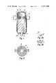
- FIG. 1is an elevation view, partly in section, of a photomultiplier tube having a photosensitive surface formed according to the present method.
- FIG. 2is a sectional view of the photomultiplier tube of FIG. 1 as seen along section lines 2--2.
- FIG. 3is a schematic view of an apparatus utilized to spherize irregular particles of photoemissive material.
- FIG. 4is a view in perspective of an apparatus used to size the spherical particles formed in the apparatus of FIG. 3.
- FIGS. 5(a) and 5(b)illustrate the formation of a substantially uniform bead by attaching spherical particles to a wire according to the present method.
- FIG. 1shows a photomultiplier tube 10 comprising an electron multiplier (not shown) and a photosensitive cathode 12 made in accordance with the present novel method.
- the photomultiplier tube 10is utilized herein by way of example, it being understood that the present invention may be applied to any device incorporating a photosensitive electrode.
- the tube 10has a cylindrical glass envelope 14 that is closed on one end by a transparent faceplate 16. The other end of the tube 10 is closed by a glass stem 18 having a number of electrical lead-in pins 20 and an exhaust tubulation 22, shown as being “tipped off”.
- a substantially cup-shaped shield 24 and adjacent the faceplate 16are beads 26 comprising a source of material used to form a photoemissive surface, such as antimony.
- a source of material used to form a photoemissive surfacesuch as antimony.
- other materials that may be used to form photoemissive surfaces when reacted with alkali metals and oxides of themselvesare tellurium, bismuth and silver. Such materials, referred to herein as "photoemissive materials”, may be used in the practice of the present novel method.
- antimony from the beads 26is deposited onto the inner surface of the faceplate 16 and a portion of the sidewall at the envelope 14.
- the shield 24confines the antimony to a preselected area at the upper end of the tube 10.
- a wire 30is arranged preferably in substantially circular form within the shield 24 and substantially concentric with the inside of the envelope 14 so that the beads 26 are symmetrical about the faceplate 16.
- a plurality of substantially equally spaced beads 26are preferably attached to the wire 30 to provide a substantially uniform deposition of antimony.
- Each of the beads 26comprises a substantially spherical particle 28 attached to a wire 30 according to a novel method of forming the beads 26.
- the spheres 28are selected to be of substantially equal diameter. It is preferred that the spherical particles 26 be formed of a platinum-antimony alloy comprising about 50% antimony and 50% platinum, by atomic volume.
- the wire 30is preferably a platinum-clad molybdenum wire but may also be a nickel or a platinum-plated tungsten wire.
- the tube 10is first evacuated until the pressure in the envelope 14 is in the order of about 10 -6 Torr or less.
- a currentis passed through the wire 30 which is connected to a pair of lead-in pins 20 to which an appropriate voltage source (not shown) is attached in order to heat the wire 30 to a sufficiently high temperature to evaporate antimony from the antimony-platinum beads 26.
- the platinumhas a vapor pressure somewhat lower than the vapor pressure of antimony, hence the platinum is not evaporated with the antimony.
- the evaporation of antimonyis continued until the antimony in the bead 26 is substantially depleted.
- the thickness of the film 32 of antimony deposited onto the substrateis determined by the amount of antimony that is contained in the spherical particles 28 attached to the wire 30.
- the thickness of the film 32can be ascertained by knowing the volume of antimony in the spherical particles 28. Measurement of light transmission through the film 32 to determine the thickness of the film 32 is not required.
- the symmetrically arranged beads 26are about the same size, the amount of antimony evaporated from each bead 26 will be nearly equal, resulting in a substantially uniform deposit over the substrate.
- the antimony film 32may then be sensitized or reacted with layers of alkali metals and additional films of antimony to achieve desired electron emission or sensitivity levels according to known photosensitizing techniques such as described, for example, in U.S. Pat. No. 3,658,400 issued on Apr. 25, 1972 or U.S. Pat. No. 3,884,539 issued on May 20, 1975.
- the formation of the beads 26 to have a predetermined amount of antimonyis obtained by the use of spherical particles 28 that are formed to very accurate dimensions.
- a commercially available process of forming the spherized particles 28is shown schematically in FIG. 3. This is known as the liquid salts bath process.
- a solution 34 of liquid saltsis contained in a quartz crucible 36 supported in a block 40.
- the top 38 of the solution 34is heated, as by an acetylene torch 42, so that the temperature of the solution at the top 38 is about 1200° C.
- the bottom 44 of the solution 34is typically about 8 inches (20.3 cm.) from the heated top 38 of the solution 34.
- the crucible 36may be rotated as by a drive motor 46 and mechanism 48 so as to uniformly heat the portion 38 of the solution 34.
- Irregular particles 50formed as by crushing a billet of platinum-antimony, as described in the prior art section, are stored above the crucible 36 in a bin 52. In this process, the irregular particles 50 are dropped into the solution 34 and allowed to drop through the solution 34. Since the melting point of platinum-antimony alloy is approximately 1080° C., the irregular particles 50 will melt upon entry into the heated solution 38 and become spherical due to their surface tension. As the particles pass into the cooler solution 44, below the melting point of the particles, the particles 28, which are not spherical, solidify and collect on the bottom of the crucible 36.
- the spherical particles 28, upon removal from the salts bath,are then sized according to their diameters.
- a method of sizing the spherical particles 28 by roller-micrometeris shown in FIG. 4.
- the roller-micrometer 54is an apparatus that can be used for accurate measurement of spheres.
- the roller-micrometer 54comprises two rollers 56 and 58 which can be adjusted to control the spacing between them. One end of the rollers is adjusted, as by a micrometer 60 to have a minimum spacing and the other end adjusted by a micrometer 62 to have a maximum opening.
- the minimum spacingmay be adjusted for 0.017 inches (0.432 mm) and the maximum set at 0.021 inches (0.533 mm).
- the spheres 28are stored in a container 64 above the end of the roller-micrometer 54 having the minimum spacing between the rollers 56 and 58.
- the rollersare rotated in a direction away from each other as shown by the arrows 66 and 68 and the spheres 28 to be sized are fed into the gap between the rollers at the close end.
- the spheres 28advance down the rollers until an opening equivalent to their diameter is reached and fall through the rollers 56 and 58 to a box 70 marked with the appropriate diameter. It is possible to measure the diameter of these spheres 28 using this technique to within several ten thousanths of an inch (several microns).
- spheres of a particular and accurate diametermay be selected for formation of the bead 26.
- the beadis formed, as shown in FIGS. 5(a) and 5(b) by heating the wire 30 to a temperature above the melting point of the sphere 28.
- the wire 30is heated to about 1200° C. in a reducing atmosphere, such as hydrogen.
- the sphere 28is then brought into contact with the heated wire 30.
- the sphere 28melts and by mutual wetting action of the platinum in the wire 30 and the sphere 28, the sphere 28 flows around the wire 30.
- a bead 26is formed that is substantially uniform, having a known quantity of antimony compared to the unknown quantity of antimony contained in beaded wire assemblies formed with an irregular shaped platinum-antimony particle.
- the novel method of forming a photosensitive electrodehas been described herein as one in which the photoemissive material in the beads 26 is evaporated to completion, it should be understood that the beads 26 comprising spheres 28 of known amounts of antimony may also be used for their capability of forming substantially uniform deposits without evaporation to depletion. Light transmission techniques may be used to monitor the deposition thickness. These measurements may be more accurate than those of the prior art in view of the fact that the antimony in the present method is deposited substantially uniformly in all directions. In certain photosensitive electrode processing, repetitive depositions of antimony films and alkali metals are required to achieve optimum sensitivity.
- a film of antimonycan be deposited substantially uniformly onto the substrate. All these spheres 28 will vaporize at nearly the same temperature and evaporate about the same amount of antimony during a given period of time. Subsequent vaporizations will continue to be nearly uniform since all the spheres 28 will have been reduced in antimony content about the same amount. This uniformity is desirable since electrons emitted from the uniformly formed photoemissive surface will be more evenly distributed, thus enhancing the quality of the tube performance.
Landscapes
- Engineering & Computer Science (AREA)
- Manufacturing & Machinery (AREA)
- Formation Of Various Coating Films On Cathode Ray Tubes And Lamps (AREA)
Abstract
Description
Claims (7)
Priority Applications (2)
| Application Number | Priority Date | Filing Date | Title |
|---|---|---|---|
| US05/973,455US4357368A (en) | 1978-12-26 | 1978-12-26 | Method of making a photosensitive electrode and a photosensitive electrode made thereby |
| JP16674079AJPS5590034A (en) | 1978-12-26 | 1979-12-20 | Method of fabricating photosensitive electrode |
Applications Claiming Priority (1)
| Application Number | Priority Date | Filing Date | Title |
|---|---|---|---|
| US05/973,455US4357368A (en) | 1978-12-26 | 1978-12-26 | Method of making a photosensitive electrode and a photosensitive electrode made thereby |
Publications (1)
| Publication Number | Publication Date |
|---|---|
| US4357368Atrue US4357368A (en) | 1982-11-02 |
Family
ID=25520913
Family Applications (1)
| Application Number | Title | Priority Date | Filing Date |
|---|---|---|---|
| US05/973,455Expired - LifetimeUS4357368A (en) | 1978-12-26 | 1978-12-26 | Method of making a photosensitive electrode and a photosensitive electrode made thereby |
Country Status (2)
| Country | Link |
|---|---|
| US (1) | US4357368A (en) |
| JP (1) | JPS5590034A (en) |
Cited By (3)
| Publication number | Priority date | Publication date | Assignee | Title |
|---|---|---|---|---|
| US5431953A (en)* | 1992-05-12 | 1995-07-11 | Hamamatsu Corporation | Automated device for applying evaporator beads to a conductive wire |
| DE4432206C1 (en)* | 1994-09-09 | 1996-02-15 | Siemens Ag | X=ray image amplifier photocathode mfr. |
| US9966594B2 (en) | 2011-06-30 | 2018-05-08 | Samsung Sdi Co., Ltd. | Negative active material, method of preparing the same, and lithium battery including negative active material |
Citations (18)
| Publication number | Priority date | Publication date | Assignee | Title |
|---|---|---|---|---|
| US1991774A (en)* | 1928-11-23 | 1935-02-19 | Old Colony Trust Company | Photoelectric tube |
| US2065570A (en)* | 1932-02-24 | 1936-12-29 | Rca Corp | Electrode structure |
| US2149977A (en)* | 1935-01-30 | 1939-03-07 | Rca Corp | Television transmitting tube |
| US2289978A (en)* | 1940-11-30 | 1942-07-14 | Rca Corp | Television picture tube screen |
| US2432657A (en)* | 1944-05-27 | 1947-12-16 | Libbey Owens Ford Glass Co | Process of evaporating metals |
| US2450856A (en)* | 1946-12-03 | 1948-10-05 | Libbey Owens Ford Glass Co | Method of coating by evaporating metals |
| US2685331A (en)* | 1951-11-26 | 1954-08-03 | Jane W Gauntlett | Child safety device |
| US2770561A (en)* | 1954-03-08 | 1956-11-13 | Rca Corp | Photoelectric cathode and method of producing same |
| US2776227A (en)* | 1953-08-19 | 1957-01-01 | Rca Corp | Method of processing a photosensitive mosaic electrode |
| US2975075A (en)* | 1956-02-17 | 1961-03-14 | Norman C Beese | Method of evaporating metals |
| US3018193A (en)* | 1958-08-13 | 1962-01-23 | Allen J Eshner | Precision thickness control for vacuum deposition of titanium and other metals for optical surfaces |
| US3063099A (en)* | 1961-01-16 | 1962-11-13 | Cons Mining & Smelting Co | Method for producing metal spheres |
| US3152246A (en)* | 1960-03-24 | 1964-10-06 | Philips Corp | Device for depositing metal layers from vapour in vacuo |
| US3658400A (en)* | 1970-03-02 | 1972-04-25 | Rca Corp | Method of making a multialkali photocathode with improved sensitivity to infrared light and a photocathode made thereby |
| US3729342A (en)* | 1969-04-16 | 1973-04-24 | Philips Corp | Method of manufacturing a radiation-sensitive electronic device |
| US3739216A (en)* | 1971-07-30 | 1973-06-12 | Zenith Radio Corp | Secondary electron multipliers with single layer cermet coatings |
| US3753023A (en)* | 1971-12-03 | 1973-08-14 | Rca Corp | Electron emissive device incorporating a secondary electron emitting material of antimony activated with potassium and cesium |
| US3884539A (en)* | 1972-12-11 | 1975-05-20 | Rca Corp | Method of making a multialkali electron emissive layer |
- 1978
- 1978-12-26USUS05/973,455patent/US4357368A/ennot_activeExpired - Lifetime
- 1979
- 1979-12-20JPJP16674079Apatent/JPS5590034A/enactivePending
Patent Citations (18)
| Publication number | Priority date | Publication date | Assignee | Title |
|---|---|---|---|---|
| US1991774A (en)* | 1928-11-23 | 1935-02-19 | Old Colony Trust Company | Photoelectric tube |
| US2065570A (en)* | 1932-02-24 | 1936-12-29 | Rca Corp | Electrode structure |
| US2149977A (en)* | 1935-01-30 | 1939-03-07 | Rca Corp | Television transmitting tube |
| US2289978A (en)* | 1940-11-30 | 1942-07-14 | Rca Corp | Television picture tube screen |
| US2432657A (en)* | 1944-05-27 | 1947-12-16 | Libbey Owens Ford Glass Co | Process of evaporating metals |
| US2450856A (en)* | 1946-12-03 | 1948-10-05 | Libbey Owens Ford Glass Co | Method of coating by evaporating metals |
| US2685331A (en)* | 1951-11-26 | 1954-08-03 | Jane W Gauntlett | Child safety device |
| US2776227A (en)* | 1953-08-19 | 1957-01-01 | Rca Corp | Method of processing a photosensitive mosaic electrode |
| US2770561A (en)* | 1954-03-08 | 1956-11-13 | Rca Corp | Photoelectric cathode and method of producing same |
| US2975075A (en)* | 1956-02-17 | 1961-03-14 | Norman C Beese | Method of evaporating metals |
| US3018193A (en)* | 1958-08-13 | 1962-01-23 | Allen J Eshner | Precision thickness control for vacuum deposition of titanium and other metals for optical surfaces |
| US3152246A (en)* | 1960-03-24 | 1964-10-06 | Philips Corp | Device for depositing metal layers from vapour in vacuo |
| US3063099A (en)* | 1961-01-16 | 1962-11-13 | Cons Mining & Smelting Co | Method for producing metal spheres |
| US3729342A (en)* | 1969-04-16 | 1973-04-24 | Philips Corp | Method of manufacturing a radiation-sensitive electronic device |
| US3658400A (en)* | 1970-03-02 | 1972-04-25 | Rca Corp | Method of making a multialkali photocathode with improved sensitivity to infrared light and a photocathode made thereby |
| US3739216A (en)* | 1971-07-30 | 1973-06-12 | Zenith Radio Corp | Secondary electron multipliers with single layer cermet coatings |
| US3753023A (en)* | 1971-12-03 | 1973-08-14 | Rca Corp | Electron emissive device incorporating a secondary electron emitting material of antimony activated with potassium and cesium |
| US3884539A (en)* | 1972-12-11 | 1975-05-20 | Rca Corp | Method of making a multialkali electron emissive layer |
Cited By (4)
| Publication number | Priority date | Publication date | Assignee | Title |
|---|---|---|---|---|
| US5431953A (en)* | 1992-05-12 | 1995-07-11 | Hamamatsu Corporation | Automated device for applying evaporator beads to a conductive wire |
| EP0569642B1 (en)* | 1992-05-12 | 1997-10-22 | Hamamatsu Corporation Inc. | Automated device for applying evaporator beads to a conductive wire |
| DE4432206C1 (en)* | 1994-09-09 | 1996-02-15 | Siemens Ag | X=ray image amplifier photocathode mfr. |
| US9966594B2 (en) | 2011-06-30 | 2018-05-08 | Samsung Sdi Co., Ltd. | Negative active material, method of preparing the same, and lithium battery including negative active material |
Also Published As
| Publication number | Publication date |
|---|---|
| JPS5590034A (en) | 1980-07-08 |
Similar Documents
| Publication | Publication Date | Title |
|---|---|---|
| Müller | Field ionization and field ion microscopy | |
| Mitchell et al. | The work functions of copper, silver and aluminium | |
| US3350595A (en) | Low dark current photoconductive device | |
| Riviere | Contact potential difference measurements by the Kelvin method | |
| US3928671A (en) | Process for fabricating a solid state, thin film field sustained conductivity device | |
| US2754259A (en) | Process and apparatus for growing single crystals | |
| Finch et al. | Crystal structure and orientation in zinc-oxide films | |
| US4724106A (en) | Process for forming organic film | |
| Colby et al. | Electrohydrodynamic ionization mass spectrometry | |
| US4357368A (en) | Method of making a photosensitive electrode and a photosensitive electrode made thereby | |
| Ashworth | Field Eflasion Microscopy | |
| Brady | The photoelectric properties of alkali metal films as a function of their thickness | |
| US4339469A (en) | Method of making potassium, cesium, rubidium, antimony photocathode | |
| US2905843A (en) | Electron discharge devices employing photo-conductive target electrodes | |
| Leverton et al. | The use of radioactive isotopes in a study of evaporation from thermionic cathodes | |
| US1832607A (en) | Photo electric tube | |
| US5264256A (en) | Apparatus and process for glow discharge comprising substrate temperature control by shutter adjustment | |
| US3499785A (en) | Coating substrates by evaporation-deposition | |
| US4568567A (en) | Method of removing trace quantities of alkali metal impurities from a bialkali-antimonide photoemissive cathode | |
| US5633562A (en) | Reflection mode alkali photocathode, and photomultiplier using the same | |
| US2829293A (en) | Lead severing contrivance | |
| US3967151A (en) | Sustained conductivity device comprising a plurality of Schottky barriers | |
| US3468807A (en) | Alkali metal generator | |
| Kiwanga | Semiconductor Adsorption on Metal Field Emitters | |
| US3015746A (en) | Electron discharge devices employing photo-conductive target electrodes |
Legal Events
| Date | Code | Title | Description |
|---|---|---|---|
| STCF | Information on status: patent grant | Free format text:PATENTED CASE | |
| CC | Certificate of correction | ||
| AS | Assignment | Owner name:NPD SUBSIDIARY INC., 38 Free format text:ASSIGNMENT OF ASSIGNORS INTEREST.;ASSIGNOR:RCA CORPORATION;REEL/FRAME:004815/0001 Effective date:19870625 | |
| AS | Assignment | Owner name:BURLE TECHNOLOGIES, INC., A CORP. OF DE Free format text:ASSIGNMENT OF ASSIGNORS INTEREST.;ASSIGNOR:BURLE INDUSTRIES, INC., A CORP. OF PA;REEL/FRAME:004940/0962 Effective date:19870728 Owner name:BURLE INDUSTRIES, INC. Free format text:MERGER;ASSIGNOR:NPD SUBSIDIARY, INC., 38;REEL/FRAME:004940/0936 Effective date:19870714 Owner name:BANCBOSTON FINANCIAL COMPANY Free format text:SECURITY INTEREST;ASSIGNOR:BURLE INDUSTRIES, INC., A CORP. OF PA;REEL/FRAME:004940/0952 Effective date:19870714 | |
| AS | Assignment | Owner name:BANCBOSTON FINANCIAL COMPANY, A MA BUSINESS TRUST Free format text:SECURITY INTEREST;ASSIGNOR:BURLE TECHNOLOGIES, INC., A DE CORPORATION;REEL/FRAME:005707/0021 Effective date:19901211 | |
| AS | Assignment | Owner name:BARCLAYS BUSINESS CREDIT, INC. Free format text:SECURITY INTEREST;ASSIGNOR:BURLE TECHNOLOGIES, INC., A DE CORP.;REEL/FRAME:006309/0001 Effective date:19911025 |