US4347447A - Current limiting MOS transistor driver circuit - Google Patents
Current limiting MOS transistor driver circuitDownload PDFInfo
- Publication number
- US4347447A US4347447AUS06/275,056US27505681AUS4347447AUS 4347447 AUS4347447 AUS 4347447AUS 27505681 AUS27505681 AUS 27505681AUS 4347447 AUS4347447 AUS 4347447A
- Authority
- US
- United States
- Prior art keywords
- transistor
- terminal
- gate
- drain
- node
- Prior art date
- Legal status (The legal status is an assumption and is not a legal conclusion. Google has not performed a legal analysis and makes no representation as to the accuracy of the status listed.)
- Expired - Lifetime
Links
Images
Classifications
- H—ELECTRICITY
- H03—ELECTRONIC CIRCUITRY
- H03K—PULSE TECHNIQUE
- H03K19/00—Logic circuits, i.e. having at least two inputs acting on one output; Inverting circuits
- H03K19/02—Logic circuits, i.e. having at least two inputs acting on one output; Inverting circuits using specified components
- H03K19/08—Logic circuits, i.e. having at least two inputs acting on one output; Inverting circuits using specified components using semiconductor devices
- H03K19/094—Logic circuits, i.e. having at least two inputs acting on one output; Inverting circuits using specified components using semiconductor devices using field-effect transistors
- H03K19/0944—Logic circuits, i.e. having at least two inputs acting on one output; Inverting circuits using specified components using semiconductor devices using field-effect transistors using MOSFET or insulated gate field-effect transistors, i.e. IGFET
- H03K19/09441—Logic circuits, i.e. having at least two inputs acting on one output; Inverting circuits using specified components using semiconductor devices using field-effect transistors using MOSFET or insulated gate field-effect transistors, i.e. IGFET of the same canal type
- H03K19/09443—Logic circuits, i.e. having at least two inputs acting on one output; Inverting circuits using specified components using semiconductor devices using field-effect transistors using MOSFET or insulated gate field-effect transistors, i.e. IGFET of the same canal type using a combination of enhancement and depletion transistors
- H—ELECTRICITY
- H03—ELECTRONIC CIRCUITRY
- H03K—PULSE TECHNIQUE
- H03K19/00—Logic circuits, i.e. having at least two inputs acting on one output; Inverting circuits
- H03K19/003—Modifications for increasing the reliability for protection
- H03K19/00315—Modifications for increasing the reliability for protection in field-effect transistor circuits
- H—ELECTRICITY
- H03—ELECTRONIC CIRCUITRY
- H03K—PULSE TECHNIQUE
- H03K19/00—Logic circuits, i.e. having at least two inputs acting on one output; Inverting circuits
- H03K19/02—Logic circuits, i.e. having at least two inputs acting on one output; Inverting circuits using specified components
- H03K19/08—Logic circuits, i.e. having at least two inputs acting on one output; Inverting circuits using specified components using semiconductor devices
- H03K19/094—Logic circuits, i.e. having at least two inputs acting on one output; Inverting circuits using specified components using semiconductor devices using field-effect transistors
- H03K19/09425—Multistate logic
- H03K19/09429—Multistate logic one of the states being the high impedance or floating state
Definitions
- the present inventionpertains to driver circuits in logic applications and more particularly pertains to such driver circuits which must have a current limited output.
- an output data stateis produced at an output terminal.
- the output terminalis then connected to deliver the output signal to other circuit elements.
- the output terminalis typically driven to high and low voltage states. If the output terminal should become grounded when the circuit is attempting to drive it to a high voltage state there may be a heavy current flow through the driving circuit. If no means are provided for limiting current flow through the output terminal, the surge of current can frequently be sufficient to damage the driving circuit.
- the provision of a current limiting resistorhas the disadvantage that it slows the driver circuit in driving the output terminal to the desired voltage state.
- a current limiting circuitwhich drives an output node to selected logic states in response to an input signal.
- a driver transistoris included in the circuit and has the gate terminal thereof connected to receive a control signal, the drain terminal thereof connected to a power terminal and the source terminal thereof connected to the output node.
- Circuitryis connected between the gate and source terminals of the driver transistor to limit the maximum voltage difference therebetween to a predetermined voltage thereby limiting the current flow through the driver transistor.
- circuitryis provided to isolate the output node to leave it in a high impedance condition.
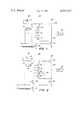
- FIG. 1is a schematic illustration of a first embodiment of a current limiting driver circuit
- FIG. 2is a schematic illustration of a second embodiment of a current limiting driver circuit.
- FIG. 1A first embodiment of a current limiting driver circuit in accordance with the present invention is illustrated in FIG. 1 and designated generally by the reference numeral 10.
- Circuit 10includes a depletion mode pull-up transistor 12 which has the gate and source terminals thereof connected to a node 14. The drain terminal of transistor 12 is connected to a first power terminal V cc .
- a pull-down transistor 16has the gate terminal connected to receive a logic level input signal ⁇ 1 .
- the drain terminal of transistor 16is connected to node 14 and the source terminal of transistor 16 is connected to ground.
- a pull-down transistor 17has the gate terminal thereof connected to receive a logic level input signal ⁇ 2 .
- the drain terminal of transistor 17is connected to node 14 and the source terminal is connected to ground.
- a transistor 18has the gate and drain terminals thereof connected to node 14.
- a transistor 20has the gate and drain terminals thereof connected to the source terminal of transistor 18.
- a transistor 22has the gate and drain terminals thereof connected to the source terminal of transistor 20. The source terminal of transistor 22 is connected to an output node 24 which is in turn connected to an output pin 26. Output data is transmitted through the pin 26.
- a driver transistor 28has the gate terminal thereof connected to node 14, the drain terminal thereof connected to the power terminal V cc and the source terminal thereof connected to the output node 24.
- a pull-down transistor 30has the gate terminal thereof connected to receive the logic level input signal ⁇ 1 , the drain terminal thereof connected to node 24 and the source terminal thereof connected to ground.
- a pull-down transistor 32has the gate terminal thereof connected to receive the ⁇ 2 input signal, the drain terminal thereof connected to the line which receives the ⁇ 1 signal and the source terminal thereof grounded.
- circuit 10Operation of circuit 10 is now described in reference to FIG. 1.
- the purpose of circuit 10is to drive the output pin 26 to a logic state determined by the state of the input signal ⁇ 1 . It is the objective of circuit 10 that the output pin be driven very quickly between the logic states and that the output pin be pulled to a high voltage state, typically one V t (voltage threshold) below the supply voltage V cc . However, there is the possibility through a system fault that the output pin 26 can become grounded when circuit 10 is attempting to drive it to a high logic state.
- V tvoltage threshold
- transistors 16 and 17 and 32When the ⁇ 1 and ⁇ 2 signals are at the low voltage state transistors 16, 17 and 32 will be turned off. When transistors 16 and 17 are turned off transistor 12 pulls node 14 to a high voltage state. Note that the maximum voltage at node 14 can be limited as described below.
- transistor 28When node 14 is at a high voltage state transistor 28 is turned on thereby pulling the output node 24 high. The ⁇ 1 signal turns off transistor 30 thereby isolating node 24 from ground. Under these conditions the output pin 26 is driven to a high voltage state.
- transistors 16 and 30When the input signal ⁇ 1 is at a high voltage state and the input signal ⁇ 2 is at a low voltage state transistors 16 and 30 will be turned on while transistors 17 and 32 will be turned off. When transistor 16 is turned on node 14 is pulled to ground which causes transistor 28 to be turned off. When transistor 30 is turned on the output node 24 is pulled to ground. The output pin 26 is thus driven to a low voltage state. When ⁇ 2 is at a low voltage state, the logic state at pin 26 is the complement of the logic state of ⁇ 1 .
- transistors 17 and 32are turned on.
- transistor 17is turned on node 14 is pulled to ground thereby turning off transistor 28.
- transistor 32is turned on the signal ⁇ 1 is forced to ground thereby turning off transistor 30.
- the output node 24is thus left floating and a high impedance condition is presented to the output pin 26.
- the output of circuit 10is disabled.
- the transistors 18, 20 and 22serve to limit the maximum voltage difference between the gate and source terminals of driver transistor 28.
- V Tcumulative threshold voltages
- transistors 18, 20 and 22these transistors will be turned on thereby providing a relatively low impedance path between nodes 14 and 24 which in turn holds down the gate-to-source voltage of transistor 28. Since the current flow through transistor 28 is a function of the gate-to-source voltage the limiting of the bias voltage serves to also limit the maximum current flow through transistor 28.
- Transistors 17 and 32are included in circuit 10 to provide a high impedance state to the output pin 26. If such a high impedance state is not required, these transistors can be deleted from circuit 10.
- each of the transistorsis designed to have a minimum channel length.
- the transistors 18, 20 and 22can have a width of 300 microns.
- the combined "on" impedance of transistors 18, 20 and 22is made substantially smaller than the "on” impedance of transistor 12 such that node 14 is limited to a maximum voltage slightly more than 3 V t above the voltage at node 24.
- FIG. 2A further embodiment of the present invention is illustrated in FIG. 2 and the circuit therein is designated generally by the reference numeral 40.
- the first logic level input signal ⁇ 1is supplied to the gate terminal of a pull-down transistor 42.
- the drain terminal of transistor 42is connected to a node 44 and the source terminal of transistor 42 is connected to ground.
- a pull-down transistor 45receives the ⁇ 2 signal at the gate terminal thereof, has the drain terminal thereof connected to node 44 and the source terminal thereof grounded.
- a pull-up depletion node transistor 46has the gate and source terminals thereof connected to node 44 and the drain terminal thereof connected to the power terminal V cc .
- Node 44is connected to the gate terminal of a driver transistor 48 which has the drain terminal thereof connected to the power terminal V cc .
- the source terminal of transistor 48is connected to an output node 50 which is in turn connected to a data output pin 52.
- a transistor 54has the gate and drain terminals thereof connected to node 44.
- a transistor 56has the gate and drain terminals thereof connected to the source terminal of transistor 54.
- a transistor 58has the gate and drain terminals thereof connected to a node 60 and the source terminal thereof connected to node 50. The source terminal of transistor 56 is connected to node 60.
- a transistor 64has the gate terminal thereof connected to node 60, the drain terminal thereof connected to node 44 and the source terminal thereof is connected to node 50.
- a pull-down transistor 66is connected to receive the logic level input signal ⁇ 1 at the gate terminal thereof.
- the drain terminal of transistor 66is connected to node 50 and the source terminal thereof is connected to ground.
- a pull-down transistor 67has the gate terminal thereof connected to receive the input signal ⁇ 2 , the drain terminal thereof connected to the line which receives the ⁇ 1 signal and the source terminal thereof connected to ground.
- a further transistor 68is connected to receive the input signal ⁇ 2 at the gate terminal thereof.
- the drain terminal of transistor 68is connected to node 60 and the source terminal of transistor 68 is connected to ground.
- circuit 40The function of circuit 40 is the same as that of circuit 10 in that the output pin 52 is driven to logic states in response to the input signal ⁇ 1 . Further, circuit means are provided for limiting the current flow through transistor 48 of circuit 40 when pin 52 is grounded.
- transistors 42, 45, 66, 67 and 68are turned off.
- node 44is pulled to a high voltage state by transistor 46.
- the high voltage state on node 44turns on transistor 48 thereby pulling node 50 to a high state.
- the low voltage state of signal ⁇ 1produces a high voltage state at the output pin 52.
- Node 50is isolated from ground since transistor 66 is turned off.
- transistors 42 and 66When the input signal ⁇ 1 is at a high voltage state and the input signal ⁇ 2 is at a low voltage state transistors 42 and 66 will be turned on while transistors 45, 67 and 68 will be turned off.
- transistor 42When transistor 42 is turned on node 44 is pulled to ground thereby turning off transistor 48.
- transistor 66When transistor 66 is turned on the output node 50 is pulled to ground thereby driving the output pin 52 to a low voltage state.
- the logic state at output 52is the complement of the logic state of signal ⁇ 1 when output disable signal ⁇ 2 is at a low voltage state.
- transistor 68When the input terminal ⁇ 2 is at a low voltage state transistor 68 is turned off thereby permitting transistors 58 and 64 to be turned on or off depending upon the voltage differential between nodes 44 and 50.
- transistors 45, 67 and 68will be turned on.
- transistor 45is turned on node 44 is pulled to a low voltage state thereby turning off transistor 48.
- transistor 67is turned on the line carrying signal ⁇ 1 is forced to ground thereby turning transistor 66 off.
- transistor 68is turned on the node 60 is pulled to a low voltage state thereby turning off transistors 64 and 58.
- transistors 48, 64, 66 and 68turned off node 50 is left in a floating condition thereby providing a high impedance to the output pin 52.
- the high impedance conditionis produced whenever the input signal ⁇ 2 goes to a high voltage state.
- the transistor 58is fabricated to have a substantially greater "on" impedance than that of either of the transistors 54 and 56.
- V Tcombined voltage thresholds
- transistors 54, 56 and 58When the gate-to-source voltage of transistor 48 exceeds the combined voltage thresholds (V T ) of transistors 54, 56 and 58, these transistors will be turned on. But when the gate-to-source voltage of transistor 48 is less than the combined voltage thresholds of transistors 54, 56 and 58, these transistors will be turned off. Since the impedance of transistor 58 is substantially greater than that of transistors 54 and 56 when all three transistors are turned on, most of the voltage difference in excess of 2 V t between nodes 44 and 50 will be developed between nodes 60 and 50.
- transistor 64This serves to turn on transistor 64 to reduce the voltage on node 44 to approximately 3 V t above that of node 50. Therefore, if node 44 should be at a high state and pin 52 should become grounded the transistors 54, 56 and 58 will be turned on thereby applying a positive bias to the gate terminal of transistor 64 which is then turned on to lower the voltage on node 44 thereby limiting the current flow through transistor 48.
- the "on" impedance of transistor 64is made to be substantially less than that of transistor 46 such that the maximum voltage on node 44 can be limited to slightly more than 3 V t above the voltage at node 50.
- circuit 40provides essentially the same function as that of circuit 10 it offers substantial space savings over that of circuit 10.
- the transistors 54 and 56can be 20 microns wide while the transistor 58 is made five microns wide.
- the transistor 64is fabricated to be 100 microns wide. It can be seen that the combined serial "on" impedance of transistors 18, 20 and 22 in FIG. 1 is essentially equal to the "on" impedance of transistor 64.
- the circuit 40utilizes approximately 145 units of area while the circuit of FIG. 1 utilizes approximately 900 units of area.
- the current limiting portion of circuit 40provides essentially the same current limiting function as circuit 10 but has approximately a factor of six savings in area on an integrated circuit chip.
- the transistors 45, 67 and 68are included in circuit 40 to provide a high impedance state to output pin 52. If such a high impedance state is not required, these transistors can be deleted from circuit 40.
- the present inventioncomprises a current limiting driver circuit in which the output terminal can be rapidly charged and pulled to a relatively high voltage state but with the provision that the maximum current through the driver transistor is limited to a predetermined safe level.
- transistors described hereinare n-channel, enhancement mode devices, however, it is recognized that an equivalent circuit can be fabricated using p-channel type devices.
Landscapes
- Engineering & Computer Science (AREA)
- Physics & Mathematics (AREA)
- Computer Hardware Design (AREA)
- Computing Systems (AREA)
- General Engineering & Computer Science (AREA)
- Mathematical Physics (AREA)
- Power Engineering (AREA)
- Logic Circuits (AREA)
Abstract
Description
Claims (15)
Priority Applications (1)
| Application Number | Priority Date | Filing Date | Title |
|---|---|---|---|
| US06/275,056US4347447A (en) | 1981-04-16 | 1981-04-16 | Current limiting MOS transistor driver circuit |
Applications Claiming Priority (2)
| Application Number | Priority Date | Filing Date | Title |
|---|---|---|---|
| US06/275,056US4347447A (en) | 1981-04-16 | 1981-04-16 | Current limiting MOS transistor driver circuit |
| PCT/US1981/000497WO1982003737A1 (en) | 1981-04-16 | 1981-04-16 | Current limiting driver circuit |
Publications (1)
| Publication Number | Publication Date |
|---|---|
| US4347447Atrue US4347447A (en) | 1982-08-31 |
Family
ID=26764478
Family Applications (1)
| Application Number | Title | Priority Date | Filing Date |
|---|---|---|---|
| US06/275,056Expired - LifetimeUS4347447A (en) | 1981-04-16 | 1981-04-16 | Current limiting MOS transistor driver circuit |
Country Status (1)
| Country | Link |
|---|---|
| US (1) | US4347447A (en) |
Cited By (32)
| Publication number | Priority date | Publication date | Assignee | Title |
|---|---|---|---|---|
| US4421994A (en)* | 1981-11-02 | 1983-12-20 | Ibm Corporation | High speed line driver with ground output capability |
| WO1984003181A1 (en)* | 1983-02-04 | 1984-08-16 | Motorola Inc | Short-protected buffer circuit |
| EP0107442A3 (en)* | 1982-10-25 | 1985-07-10 | Kabushiki Kaisha Toshiba | Signal input circuit |
| US4543494A (en)* | 1981-12-29 | 1985-09-24 | Fujitsu Limited | MOS type output driver circuit having a protective circuit |
| US4581551A (en)* | 1984-03-28 | 1986-04-08 | Motorola, Inc. | Input/output circuit for use with various voltages |
| US4587446A (en)* | 1982-05-28 | 1986-05-06 | Nec Corporation | Field effect transistor output circuit operable by a reduced amount of current |
| US4631426A (en)* | 1984-06-27 | 1986-12-23 | Honeywell Inc. | Digital circuit using MESFETS |
| US4810969A (en)* | 1987-06-23 | 1989-03-07 | Honeywell Inc. | High speed logic circuit having feedback to prevent current in the output stage |
| US4985644A (en)* | 1987-11-26 | 1991-01-15 | Mitsubishi Denki Kabushiki Kaisha | Output buffer semiconductor and method for controlling current flow in an output switching device |
| US4996449A (en)* | 1988-07-19 | 1991-02-26 | Kabushiki Kaisha Toshiba | Output circuit having high speed operation and low power dissipation |
| US5160858A (en)* | 1990-10-11 | 1992-11-03 | Kabushiki Kaisha Toshiba | Field-effect transistor circuit |
| EP0545361A1 (en)* | 1991-12-06 | 1993-06-09 | National Semiconductor Corporation | State dependent discharge path circuit |
| US5229659A (en)* | 1991-10-16 | 1993-07-20 | National Semiconductor Corporation | Low power complementary mosfet digital signal buffer circuit |
| US5281869A (en)* | 1992-07-01 | 1994-01-25 | Digital Equipment Corporation | Reduced-voltage NMOS output driver |
| US5347179A (en)* | 1993-04-15 | 1994-09-13 | Micron Semiconductor, Inc. | Inverting output driver circuit for reducing electron injection into the substrate |
| US5355032A (en)* | 1993-03-24 | 1994-10-11 | Sun Microsystems, Inc. | TTL to CMOS translator circuit and method |
| US5359240A (en)* | 1993-01-25 | 1994-10-25 | National Semiconductor Corporation | Low power digital signal buffer circuit |
| JPH0698039B2 (en)* | 1983-12-12 | 1994-12-07 | エイチ・ア−ル・アイ・リサ−チ・インコ−ポレ−テッド | Nucleic acid hybridization test |
| US5386336A (en)* | 1992-06-19 | 1995-01-31 | Trw Inc. | On chip current limiter |
| WO1995022204A1 (en)* | 1994-02-14 | 1995-08-17 | Cascade Design Automation Corp. | High-speed solid state buffer circuit and method for producing the same |
| US5537072A (en)* | 1994-06-30 | 1996-07-16 | Sgs-Thomson Microelectronics, Inc. | Charge pump switch circuits |
| US5545934A (en)* | 1994-12-22 | 1996-08-13 | Alliance Semiconductor Corporation | Voltage clamp circuit |
| US5646551A (en)* | 1995-08-07 | 1997-07-08 | Etron Technology Inc. | Mixed mode output buffer circuit for CMOSIC |
| US5955915A (en)* | 1995-03-28 | 1999-09-21 | Stmicroelectronics, Inc. | Circuit for limiting the current in a power transistor |
| US5959481A (en)* | 1997-02-18 | 1999-09-28 | Rambus Inc. | Bus driver circuit including a slew rate indicator circuit having a one shot circuit |
| US5963023A (en)* | 1998-03-21 | 1999-10-05 | Advanced Micro Devices, Inc. | Power surge management for high performance integrated circuit |
| US5963076A (en)* | 1997-04-14 | 1999-10-05 | Motorola, Inc. | Circuit with hot-electron protection and method |
| US5966038A (en)* | 1997-12-15 | 1999-10-12 | Motorola, Inc. | Circuit with overvoltage protection |
| US20040041151A1 (en)* | 2002-08-27 | 2004-03-04 | Semiconductor Components Industries, Llc. | Method of forming a power device and structure therefor |
| US7613237B1 (en)* | 2005-01-13 | 2009-11-03 | Advanced Micro Devices, Inc. | Built-in test feature to facilitate system level stress testing of a high-speed serial link that uses a forwarding clock |
| CN106301318A (en)* | 2015-05-12 | 2017-01-04 | 中车大连电力牵引研发中心有限公司 | The isolated drive circuit of MOSFET element |
| US20240332959A1 (en)* | 2023-03-28 | 2024-10-03 | Yangtze Memory Technologies Co., Ltd. | Electrostatic protection circuit, memory device, memory system, and electrostatic protection method |
Citations (6)
| Publication number | Priority date | Publication date | Assignee | Title |
|---|---|---|---|---|
| US3651340A (en)* | 1970-06-22 | 1972-03-21 | Hamilton Watch Co | Current limiting complementary symmetry mos inverters |
| US3906255A (en)* | 1974-09-06 | 1975-09-16 | Motorola Inc | MOS current limiting output circuit |
| US3913026A (en)* | 1974-04-08 | 1975-10-14 | Bulova Watch Co Inc | Mos transistor gain block |
| US4065678A (en)* | 1976-07-02 | 1977-12-27 | Motorola, Inc. | Clamped push-pull driver circuit with output feedback |
| US4096398A (en)* | 1977-02-23 | 1978-06-20 | National Semiconductor Corporation | MOS output buffer circuit with feedback |
| US4275313A (en)* | 1979-04-09 | 1981-06-23 | Bell Telephone Laboratories, Incorporated | Current limiting output circuit with output feedback |
- 1981
- 1981-04-16USUS06/275,056patent/US4347447A/ennot_activeExpired - Lifetime
Patent Citations (6)
| Publication number | Priority date | Publication date | Assignee | Title |
|---|---|---|---|---|
| US3651340A (en)* | 1970-06-22 | 1972-03-21 | Hamilton Watch Co | Current limiting complementary symmetry mos inverters |
| US3913026A (en)* | 1974-04-08 | 1975-10-14 | Bulova Watch Co Inc | Mos transistor gain block |
| US3906255A (en)* | 1974-09-06 | 1975-09-16 | Motorola Inc | MOS current limiting output circuit |
| US4065678A (en)* | 1976-07-02 | 1977-12-27 | Motorola, Inc. | Clamped push-pull driver circuit with output feedback |
| US4096398A (en)* | 1977-02-23 | 1978-06-20 | National Semiconductor Corporation | MOS output buffer circuit with feedback |
| US4275313A (en)* | 1979-04-09 | 1981-06-23 | Bell Telephone Laboratories, Incorporated | Current limiting output circuit with output feedback |
Non-Patent Citations (1)
| Title |
|---|
| Homan, "FET Depletion Load Push-Pull Logical Circuit"; IBM Tech. Discl. Bull.; vol. 18, No. 3, pp. 910-911; 8/1975. |
Cited By (37)
| Publication number | Priority date | Publication date | Assignee | Title |
|---|---|---|---|---|
| US4421994A (en)* | 1981-11-02 | 1983-12-20 | Ibm Corporation | High speed line driver with ground output capability |
| US4543494A (en)* | 1981-12-29 | 1985-09-24 | Fujitsu Limited | MOS type output driver circuit having a protective circuit |
| US4587446A (en)* | 1982-05-28 | 1986-05-06 | Nec Corporation | Field effect transistor output circuit operable by a reduced amount of current |
| EP0107442A3 (en)* | 1982-10-25 | 1985-07-10 | Kabushiki Kaisha Toshiba | Signal input circuit |
| WO1984003181A1 (en)* | 1983-02-04 | 1984-08-16 | Motorola Inc | Short-protected buffer circuit |
| JPH0698039B2 (en)* | 1983-12-12 | 1994-12-07 | エイチ・ア−ル・アイ・リサ−チ・インコ−ポレ−テッド | Nucleic acid hybridization test |
| US4581551A (en)* | 1984-03-28 | 1986-04-08 | Motorola, Inc. | Input/output circuit for use with various voltages |
| US4631426A (en)* | 1984-06-27 | 1986-12-23 | Honeywell Inc. | Digital circuit using MESFETS |
| US4810969A (en)* | 1987-06-23 | 1989-03-07 | Honeywell Inc. | High speed logic circuit having feedback to prevent current in the output stage |
| US4985644A (en)* | 1987-11-26 | 1991-01-15 | Mitsubishi Denki Kabushiki Kaisha | Output buffer semiconductor and method for controlling current flow in an output switching device |
| US4996449A (en)* | 1988-07-19 | 1991-02-26 | Kabushiki Kaisha Toshiba | Output circuit having high speed operation and low power dissipation |
| US5160858A (en)* | 1990-10-11 | 1992-11-03 | Kabushiki Kaisha Toshiba | Field-effect transistor circuit |
| US5229659A (en)* | 1991-10-16 | 1993-07-20 | National Semiconductor Corporation | Low power complementary mosfet digital signal buffer circuit |
| EP0545361A1 (en)* | 1991-12-06 | 1993-06-09 | National Semiconductor Corporation | State dependent discharge path circuit |
| US5386336A (en)* | 1992-06-19 | 1995-01-31 | Trw Inc. | On chip current limiter |
| US5281869A (en)* | 1992-07-01 | 1994-01-25 | Digital Equipment Corporation | Reduced-voltage NMOS output driver |
| US5359240A (en)* | 1993-01-25 | 1994-10-25 | National Semiconductor Corporation | Low power digital signal buffer circuit |
| US5355032A (en)* | 1993-03-24 | 1994-10-11 | Sun Microsystems, Inc. | TTL to CMOS translator circuit and method |
| US5347179A (en)* | 1993-04-15 | 1994-09-13 | Micron Semiconductor, Inc. | Inverting output driver circuit for reducing electron injection into the substrate |
| USRE35764E (en)* | 1993-04-15 | 1998-04-07 | Micron Technology, Inc. | Inverting output driver circuit for reducing electron injection into the substrate |
| WO1995022204A1 (en)* | 1994-02-14 | 1995-08-17 | Cascade Design Automation Corp. | High-speed solid state buffer circuit and method for producing the same |
| US5537072A (en)* | 1994-06-30 | 1996-07-16 | Sgs-Thomson Microelectronics, Inc. | Charge pump switch circuits |
| US5545934A (en)* | 1994-12-22 | 1996-08-13 | Alliance Semiconductor Corporation | Voltage clamp circuit |
| US5955915A (en)* | 1995-03-28 | 1999-09-21 | Stmicroelectronics, Inc. | Circuit for limiting the current in a power transistor |
| US5646551A (en)* | 1995-08-07 | 1997-07-08 | Etron Technology Inc. | Mixed mode output buffer circuit for CMOSIC |
| US5959481A (en)* | 1997-02-18 | 1999-09-28 | Rambus Inc. | Bus driver circuit including a slew rate indicator circuit having a one shot circuit |
| US5963076A (en)* | 1997-04-14 | 1999-10-05 | Motorola, Inc. | Circuit with hot-electron protection and method |
| US5966038A (en)* | 1997-12-15 | 1999-10-12 | Motorola, Inc. | Circuit with overvoltage protection |
| US5963023A (en)* | 1998-03-21 | 1999-10-05 | Advanced Micro Devices, Inc. | Power surge management for high performance integrated circuit |
| US20040041151A1 (en)* | 2002-08-27 | 2004-03-04 | Semiconductor Components Industries, Llc. | Method of forming a power device and structure therefor |
| US6809559B2 (en)* | 2002-08-27 | 2004-10-26 | Semiconductor Components Industries, L.L.C. | Method of forming a power device and structure therefor |
| CN100339960C (en)* | 2002-08-27 | 2007-09-26 | 半导体元件工业有限责任公司 | Method for forming power devices and structure thereof |
| US7613237B1 (en)* | 2005-01-13 | 2009-11-03 | Advanced Micro Devices, Inc. | Built-in test feature to facilitate system level stress testing of a high-speed serial link that uses a forwarding clock |
| CN106301318A (en)* | 2015-05-12 | 2017-01-04 | 中车大连电力牵引研发中心有限公司 | The isolated drive circuit of MOSFET element |
| CN106301318B (en)* | 2015-05-12 | 2023-07-18 | 中车大连电力牵引研发中心有限公司 | Isolation driving circuit of MOSFET device |
| US20240332959A1 (en)* | 2023-03-28 | 2024-10-03 | Yangtze Memory Technologies Co., Ltd. | Electrostatic protection circuit, memory device, memory system, and electrostatic protection method |
| US12424847B2 (en)* | 2023-03-28 | 2025-09-23 | Yangtze Memory Technologies Co., Ltd. | Electrostatic protection circuit, memory device, memory system, and electrostatic protection method |
Similar Documents
| Publication | Publication Date | Title |
|---|---|---|
| US4347447A (en) | Current limiting MOS transistor driver circuit | |
| US5555149A (en) | Overvoltage protection | |
| KR940003809B1 (en) | Ttl to cmos input buffer | |
| US5900741A (en) | CMOS buffer having stable threshold voltage | |
| JPH0720060B2 (en) | Output circuit device | |
| US6300800B1 (en) | Integrated circuit I/O buffer with series P-channel and floating well | |
| KR960011964B1 (en) | Output buffer device | |
| US5723987A (en) | Level shifting output buffer with p channel pulldown transistors which are bypassed | |
| EP0260389A2 (en) | Off-chip driver circuits | |
| US11004843B2 (en) | Switch control circuit for a power switch with electrostatic discharge (ESD) protection | |
| US6069515A (en) | High voltage input buffer circuit using low voltage transistors | |
| US4810969A (en) | High speed logic circuit having feedback to prevent current in the output stage | |
| US5966035A (en) | High voltage tolerable input buffer | |
| KR100363381B1 (en) | Two-supply protection circuit | |
| US6225838B1 (en) | Integrated circuit buffers having reduced power consumption requirements | |
| EP0695037A1 (en) | Off-chip driver circuit | |
| JPH05227010A (en) | Floating well cmos output driver | |
| JP2918821B2 (en) | Off-chip driver circuit | |
| US4296340A (en) | Initializing circuit for MOS integrated circuits | |
| US5432463A (en) | High speed NOR gate with small output voltage swings | |
| US4503341A (en) | Power-down inverter circuit | |
| EP0619652A2 (en) | Data output circuit | |
| EP0840453A2 (en) | An output buffer | |
| KR0129592B1 (en) | Low noise output buffer | |
| EP0610621A2 (en) | Digital logic circuit and method having pull-down and pull-up devices |
Legal Events
| Date | Code | Title | Description |
|---|---|---|---|
| AS | Assignment | Owner name:MOSTEK CORPORATION, 1215 WEST CROSBY RD. CARROLLTO Free format text:ASSIGNMENT OF ASSIGNORS INTEREST.;ASSIGNOR:PROEBSTING, ROBERT J.;REEL/FRAME:003895/0533 Effective date:19810407 | |
| STCF | Information on status: patent grant | Free format text:PATENTED CASE | |
| MAFP | Maintenance fee payment | Free format text:PAYMENT OF MAINTENANCE FEE, 4TH YEAR, PL 96-517 (ORIGINAL EVENT CODE: M170); ENTITY STATUS OF PATENT OWNER: LARGE ENTITY Year of fee payment:4 | |
| AS | Assignment | Owner name:THOMSON COMPONENTS-MOSTEK CORPORATION Free format text:ASSIGNMENT OF ASSIGNORS INTEREST.;ASSIGNOR:CTU OF DELAWARE, INC., FORMERLY MOSTEK CORPORATION;REEL/FRAME:004810/0156 Effective date:19870721 | |
| AS | Assignment | Owner name:SGS-THOMSON MICROELECTRONICS, INC. Free format text:CHANGE OF NAME;ASSIGNOR:THOMSON COMPONENTS-MOSTEK CORPORATION;REEL/FRAME:005270/0714 Effective date:19871023 Owner name:SGS-THOMSON MICROELECTRONICS, INC. Free format text:MERGER;ASSIGNORS:SGS SEMICONDUCTOR CORPORATION, A CORP. OF DE;THOMSON HOLDINGS (DELAWARE) INC., A CORP. OF DE;SGS-THOMSON MICROELECTRONICS, INC. A CORP. OF DE (MERGED INTO);REEL/FRAME:005270/0725 Effective date:19871224 | |
| MAFP | Maintenance fee payment | Free format text:PAYMENT OF MAINTENANCE FEE, 8TH YEAR, PL 96-517 (ORIGINAL EVENT CODE: M171); ENTITY STATUS OF PATENT OWNER: LARGE ENTITY Year of fee payment:8 | |
| FEPP | Fee payment procedure | Free format text:PAYOR NUMBER ASSIGNED (ORIGINAL EVENT CODE: ASPN); ENTITY STATUS OF PATENT OWNER: LARGE ENTITY | |
| MAFP | Maintenance fee payment | Free format text:PAYMENT OF MAINTENANCE FEE, 12TH YEAR, LARGE ENTITY (ORIGINAL EVENT CODE: M185); ENTITY STATUS OF PATENT OWNER: LARGE ENTITY Year of fee payment:12 | |
| FEPP | Fee payment procedure | Free format text:PAYOR NUMBER ASSIGNED (ORIGINAL EVENT CODE: ASPN); ENTITY STATUS OF PATENT OWNER: LARGE ENTITY Free format text:PAYER NUMBER DE-ASSIGNED (ORIGINAL EVENT CODE: RMPN); ENTITY STATUS OF PATENT OWNER: LARGE ENTITY |