US4342617A - Process for forming opening having tapered sides in a plasma nitride layer - Google Patents
Process for forming opening having tapered sides in a plasma nitride layerDownload PDFInfo
- Publication number
- US4342617A US4342617AUS06/236,833US23683381AUS4342617AUS 4342617 AUS4342617 AUS 4342617AUS 23683381 AUS23683381 AUS 23683381AUS 4342617 AUS4342617 AUS 4342617A
- Authority
- US
- United States
- Prior art keywords
- layer
- plasma nitride
- opening
- nitride layer
- plasma
- Prior art date
- Legal status (The legal status is an assumption and is not a legal conclusion. Google has not performed a legal analysis and makes no representation as to the accuracy of the status listed.)
- Expired - Lifetime
Links
Images


Classifications
- H—ELECTRICITY
- H01—ELECTRIC ELEMENTS
- H01L—SEMICONDUCTOR DEVICES NOT COVERED BY CLASS H10
- H01L21/00—Processes or apparatus adapted for the manufacture or treatment of semiconductor or solid state devices or of parts thereof
- H01L21/02—Manufacture or treatment of semiconductor devices or of parts thereof
- H01L21/02104—Forming layers
- H01L21/02107—Forming insulating materials on a substrate
- H01L21/02225—Forming insulating materials on a substrate characterised by the process for the formation of the insulating layer
- H01L21/0226—Forming insulating materials on a substrate characterised by the process for the formation of the insulating layer formation by a deposition process
- H01L21/02263—Forming insulating materials on a substrate characterised by the process for the formation of the insulating layer formation by a deposition process deposition from the gas or vapour phase
- H01L21/02271—Forming insulating materials on a substrate characterised by the process for the formation of the insulating layer formation by a deposition process deposition from the gas or vapour phase deposition by decomposition or reaction of gaseous or vapour phase compounds, i.e. chemical vapour deposition
- H01L21/02274—Forming insulating materials on a substrate characterised by the process for the formation of the insulating layer formation by a deposition process deposition from the gas or vapour phase deposition by decomposition or reaction of gaseous or vapour phase compounds, i.e. chemical vapour deposition in the presence of a plasma [PECVD]
- C—CHEMISTRY; METALLURGY
- C23—COATING METALLIC MATERIAL; COATING MATERIAL WITH METALLIC MATERIAL; CHEMICAL SURFACE TREATMENT; DIFFUSION TREATMENT OF METALLIC MATERIAL; COATING BY VACUUM EVAPORATION, BY SPUTTERING, BY ION IMPLANTATION OR BY CHEMICAL VAPOUR DEPOSITION, IN GENERAL; INHIBITING CORROSION OF METALLIC MATERIAL OR INCRUSTATION IN GENERAL
- C23C—COATING METALLIC MATERIAL; COATING MATERIAL WITH METALLIC MATERIAL; SURFACE TREATMENT OF METALLIC MATERIAL BY DIFFUSION INTO THE SURFACE, BY CHEMICAL CONVERSION OR SUBSTITUTION; COATING BY VACUUM EVAPORATION, BY SPUTTERING, BY ION IMPLANTATION OR BY CHEMICAL VAPOUR DEPOSITION, IN GENERAL
- C23C16/00—Chemical coating by decomposition of gaseous compounds, without leaving reaction products of surface material in the coating, i.e. chemical vapour deposition [CVD] processes
- C23C16/22—Chemical coating by decomposition of gaseous compounds, without leaving reaction products of surface material in the coating, i.e. chemical vapour deposition [CVD] processes characterised by the deposition of inorganic material, other than metallic material
- C23C16/30—Deposition of compounds, mixtures or solid solutions, e.g. borides, carbides, nitrides
- C23C16/34—Nitrides
- C23C16/345—Silicon nitride
- H—ELECTRICITY
- H01—ELECTRIC ELEMENTS
- H01L—SEMICONDUCTOR DEVICES NOT COVERED BY CLASS H10
- H01L21/00—Processes or apparatus adapted for the manufacture or treatment of semiconductor or solid state devices or of parts thereof
- H01L21/02—Manufacture or treatment of semiconductor devices or of parts thereof
- H01L21/02104—Forming layers
- H01L21/02107—Forming insulating materials on a substrate
- H01L21/02109—Forming insulating materials on a substrate characterised by the type of layer, e.g. type of material, porous/non-porous, pre-cursors, mixtures or laminates
- H01L21/02112—Forming insulating materials on a substrate characterised by the type of layer, e.g. type of material, porous/non-porous, pre-cursors, mixtures or laminates characterised by the material of the layer
- H01L21/02123—Forming insulating materials on a substrate characterised by the type of layer, e.g. type of material, porous/non-porous, pre-cursors, mixtures or laminates characterised by the material of the layer the material containing silicon
- H01L21/0217—Forming insulating materials on a substrate characterised by the type of layer, e.g. type of material, porous/non-porous, pre-cursors, mixtures or laminates characterised by the material of the layer the material containing silicon the material being a silicon nitride not containing oxygen, e.g. SixNy or SixByNz
- H—ELECTRICITY
- H01—ELECTRIC ELEMENTS
- H01L—SEMICONDUCTOR DEVICES NOT COVERED BY CLASS H10
- H01L21/00—Processes or apparatus adapted for the manufacture or treatment of semiconductor or solid state devices or of parts thereof
- H01L21/02—Manufacture or treatment of semiconductor devices or of parts thereof
- H01L21/02104—Forming layers
- H01L21/02107—Forming insulating materials on a substrate
- H01L21/02109—Forming insulating materials on a substrate characterised by the type of layer, e.g. type of material, porous/non-porous, pre-cursors, mixtures or laminates
- H01L21/02205—Forming insulating materials on a substrate characterised by the type of layer, e.g. type of material, porous/non-porous, pre-cursors, mixtures or laminates the layer being characterised by the precursor material for deposition
- H01L21/02208—Forming insulating materials on a substrate characterised by the type of layer, e.g. type of material, porous/non-porous, pre-cursors, mixtures or laminates the layer being characterised by the precursor material for deposition the precursor containing a compound comprising Si
- H01L21/02211—Forming insulating materials on a substrate characterised by the type of layer, e.g. type of material, porous/non-porous, pre-cursors, mixtures or laminates the layer being characterised by the precursor material for deposition the precursor containing a compound comprising Si the compound being a silane, e.g. disilane, methylsilane or chlorosilane
- H—ELECTRICITY
- H01—ELECTRIC ELEMENTS
- H01L—SEMICONDUCTOR DEVICES NOT COVERED BY CLASS H10
- H01L21/00—Processes or apparatus adapted for the manufacture or treatment of semiconductor or solid state devices or of parts thereof
- H01L21/02—Manufacture or treatment of semiconductor devices or of parts thereof
- H01L21/04—Manufacture or treatment of semiconductor devices or of parts thereof the devices having potential barriers, e.g. a PN junction, depletion layer or carrier concentration layer
- H01L21/18—Manufacture or treatment of semiconductor devices or of parts thereof the devices having potential barriers, e.g. a PN junction, depletion layer or carrier concentration layer the devices having semiconductor bodies comprising elements of Group IV of the Periodic Table or AIIIBV compounds with or without impurities, e.g. doping materials
- H01L21/30—Treatment of semiconductor bodies using processes or apparatus not provided for in groups H01L21/20 - H01L21/26
- H01L21/31—Treatment of semiconductor bodies using processes or apparatus not provided for in groups H01L21/20 - H01L21/26 to form insulating layers thereon, e.g. for masking or by using photolithographic techniques; After treatment of these layers; Selection of materials for these layers
- H01L21/3105—After-treatment
- H01L21/311—Etching the insulating layers by chemical or physical means
- H01L21/31105—Etching inorganic layers
- H01L21/31111—Etching inorganic layers by chemical means
- H—ELECTRICITY
- H01—ELECTRIC ELEMENTS
- H01L—SEMICONDUCTOR DEVICES NOT COVERED BY CLASS H10
- H01L21/00—Processes or apparatus adapted for the manufacture or treatment of semiconductor or solid state devices or of parts thereof
- H01L21/70—Manufacture or treatment of devices consisting of a plurality of solid state components formed in or on a common substrate or of parts thereof; Manufacture of integrated circuit devices or of parts thereof
- H01L21/71—Manufacture of specific parts of devices defined in group H01L21/70
- H01L21/768—Applying interconnections to be used for carrying current between separate components within a device comprising conductors and dielectrics
- H01L21/76801—Applying interconnections to be used for carrying current between separate components within a device comprising conductors and dielectrics characterised by the formation and the after-treatment of the dielectrics, e.g. smoothing
- H01L21/76802—Applying interconnections to be used for carrying current between separate components within a device comprising conductors and dielectrics characterised by the formation and the after-treatment of the dielectrics, e.g. smoothing by forming openings in dielectrics
- H01L21/76804—Applying interconnections to be used for carrying current between separate components within a device comprising conductors and dielectrics characterised by the formation and the after-treatment of the dielectrics, e.g. smoothing by forming openings in dielectrics by forming tapered via holes
- H—ELECTRICITY
- H01—ELECTRIC ELEMENTS
- H01L—SEMICONDUCTOR DEVICES NOT COVERED BY CLASS H10
- H01L21/00—Processes or apparatus adapted for the manufacture or treatment of semiconductor or solid state devices or of parts thereof
- H01L21/02—Manufacture or treatment of semiconductor devices or of parts thereof
- H01L21/02104—Forming layers
- H01L21/02107—Forming insulating materials on a substrate
- H01L21/02109—Forming insulating materials on a substrate characterised by the type of layer, e.g. type of material, porous/non-porous, pre-cursors, mixtures or laminates
- H01L21/02112—Forming insulating materials on a substrate characterised by the type of layer, e.g. type of material, porous/non-porous, pre-cursors, mixtures or laminates characterised by the material of the layer
- H01L21/02123—Forming insulating materials on a substrate characterised by the type of layer, e.g. type of material, porous/non-porous, pre-cursors, mixtures or laminates characterised by the material of the layer the material containing silicon
- H01L21/02164—Forming insulating materials on a substrate characterised by the type of layer, e.g. type of material, porous/non-porous, pre-cursors, mixtures or laminates characterised by the material of the layer the material containing silicon the material being a silicon oxide, e.g. SiO2
Definitions
- the inventionrelates to the field of forming contact openings in insulative layers, particularly plasma nitride layers used in the fabrication of semiconductor devices.
- Plasma nitrideSi x /N y
- Si x /N yPlasma nitride
- the present inventiondescribes a process for forming a plasma nitride layer and opening therethrough which opening has tapered sides. This more readily permits the forming of contacts in the opening since better metal flow is obtained and high stress regions are minimized.
- a process for forming a plasma nitride layer with an opening therethrough where the opening has tapered sidesis described.
- the opening with its tapered sidesis suitable for receiving a metal contact as the tapered sides provides better metal flow and reduces high stress regions within the metal.
- a first layer of plasma nitrideis formed. Over this first layer, a second layer of plasma nitride is formed; the second layer having a higher etching rate than the first layer.
- an openingis etched through the first and second layers of plasma nitride (or plasma oxynitride) with an ordinary masking member. The second layer etches at a faster rate than the first layer thereby providing an opening with tapered sides.
- the first and second layers of plasma nitrideare integrally formed, and the higher etching rate of the upper portion of the layer is obtained by using more silicon.
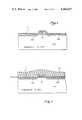
- FIG. 1is a cross-sectional elevation view of a portion of a substrate which includes a gate member, source and drain regions with an overlying oxide layer.
- FIG. 2illustrates the substrate of FIG. 1 with a first plasma nitride layer formed thereon.
- FIG. 3illustrates the substrate of FIG. 2 with a second plasma layer formed thereon.
- FIG. 4illustrates the substrate of FIG. 3 after the formation of a photoresist layer and the formation of an opening through this layer. Note that the cross-sectional elevation view of FIG. 4 is shifted from the view of FIGS. 1 through 3 to better illustrate the region of the substrate lying to the left of the gate member.
- FIG. 5illustrates the substrate of FIG. 4 after an opening having tapered sides has been etched through the plasma nitride layers.
- FIG. 6illustrates the substrate of FIG. 5 after an opening has been etched through the oxide layer and an ohmic contact formed in the opening.
- FIG. 7is a photograph from a scanning electron microscope which shows an actual plasma nitride layer and opening made with the process of the present invention.
- openings through plasma nitride layersare described which provides contact to an underlying substrate region. It will be obvious that openings through plasma nitride layers may be formed in the described manner for interconnecting metal layers, polysilicon layers, polysilicon to metal layers, and other interconnections.
- a substrate 10is illustrated, which for the described embodiment, is a p-type monocrystalline silicon substrate (50 ohm-cm.) having a crystalline orientation of (100).
- MOSmetal-oxide-semiconductor
- a polysilicon gate member 14is formed over the substrate which is insulated from the substrate by a gate oxide layer 16.
- Source and drain regions 12a and 12bare formed in alignment with the polysilicon gate member 14. Then an additional oxide layer 17 is grown over the substrate.
- the gate oxide layer 16may have a thickness of approximately 250 A, the gate member 14 a thickness of approximately 3000 A, and the source and drain regions doped to a level of approximately 10 20 /cm 3 ion implantation with arsenic.
- the layer 17is formed with a re-oxidation step and in the presently preferred embodiment, is approximately 700 A thick.
- a plasma nitride (SiNy) layer 20 of approximately 1 micronis formed over the oxide layer 17 with a known process.
- Silane (SiH 4 ) and ammonia (NH 3 )are used in a reactor to form the plasma nitride.
- the processis available from Pacific Western, Elko, Nev.
- a second layer 21 of plasma nitrideis formed over the layer 20.
- the second layer 21is substantially thinner than the layer 20 and importantly, has a faster etching rate than the layer 20.
- the layer 21 in the presently preferred embodimentis approximately 500-1000 A thick.
- the layers 20 and 21are integrally formed without removing the wafers from the reactor.
- a richer silane mixtureis used to form the upper portion of the layer (layer 21).
- a flow rate of 350 ml/min. of silaneis used, along with a flow rate of 415 ml/min. of ammonia.
- the flow of ammoniais reduced to approximately 300 ml/min.
- a photoresist layer 23is formed over the layer 21.
- This layermay be approximately 1.8 microns thick and formed with a positive photoresist.
- An opening 25is formed through the layer 23 using ordinary photolithorgraphic techniques. This opening is formed above the region 12a.
- a plasma nitride etchantis used to etch through the layers 20 and 21 in a single ordinary dry etching step (plasma etchant).
- the oxide layer 17 at the region 26forms an etchant stop and prevents the etchant from attacking the substrate.
- an oxide etchantis used to etch through the oxide layer 17 at the opening 25 and then the photoresist layer is removed.
- a metal contactsuch as an aluminum silicon alloy contact 30 is formed in contact with the region 12a.
- the tapered openingeliminates the sharp corners thereby providing better metal flow and reduced high stress regions.
- the sides of the openingare at an angle of approximately 45 degrees to 55 degrees with respect to the substrate. This slope is obtained even though the faster etching plasma nitride is only 500-1000 A thick.
- FIG. 7an actual opening formed with the above-described process is shown.
- the substrate with its doped regionis clearly seen as is the plasma nitride layer.
- the smooth taper of the opening through the plasma nitride regionis vividly illustrated.
- the trace line in the upper right-hand corner of the photographis 1 micron in length.
- a doped regionmay be necessary below the contact 30 to prevent "spiking" as is well-known in the prior art.
- Such regionwhere necessary may be formed with the processing steps used to form buried contact regions, or a separate masking and doping step may be used before the formation of the layer 20.
- the invented processmay be used to form contacts between a metal or polysilicon layer and a substrate, between polysilicon layers and metal layers, and metal and polysilicon layers. Ohmic contacts of metal (or polysilicon) or like contacts can be made then, more reliably.
Landscapes
- Engineering & Computer Science (AREA)
- Chemical & Material Sciences (AREA)
- Physics & Mathematics (AREA)
- Condensed Matter Physics & Semiconductors (AREA)
- General Physics & Mathematics (AREA)
- Manufacturing & Machinery (AREA)
- Computer Hardware Design (AREA)
- Microelectronics & Electronic Packaging (AREA)
- Power Engineering (AREA)
- Chemical Kinetics & Catalysis (AREA)
- General Chemical & Material Sciences (AREA)
- Inorganic Chemistry (AREA)
- Plasma & Fusion (AREA)
- Materials Engineering (AREA)
- Mechanical Engineering (AREA)
- Metallurgy (AREA)
- Organic Chemistry (AREA)
- Electrodes Of Semiconductors (AREA)
- Drying Of Semiconductors (AREA)
Abstract
Description
Claims (6)
Priority Applications (1)
| Application Number | Priority Date | Filing Date | Title |
|---|---|---|---|
| US06/236,833US4342617A (en) | 1981-02-23 | 1981-02-23 | Process for forming opening having tapered sides in a plasma nitride layer |
Applications Claiming Priority (1)
| Application Number | Priority Date | Filing Date | Title |
|---|---|---|---|
| US06/236,833US4342617A (en) | 1981-02-23 | 1981-02-23 | Process for forming opening having tapered sides in a plasma nitride layer |
Publications (1)
| Publication Number | Publication Date |
|---|---|
| US4342617Atrue US4342617A (en) | 1982-08-03 |
Family
ID=22891152
Family Applications (1)
| Application Number | Title | Priority Date | Filing Date |
|---|---|---|---|
| US06/236,833Expired - LifetimeUS4342617A (en) | 1981-02-23 | 1981-02-23 | Process for forming opening having tapered sides in a plasma nitride layer |
Country Status (1)
| Country | Link |
|---|---|
| US (1) | US4342617A (en) |
Cited By (29)
| Publication number | Priority date | Publication date | Assignee | Title |
|---|---|---|---|---|
| US4603056A (en)* | 1985-04-25 | 1986-07-29 | International Business Machines Corporation | Surface treatment of a molybdenum screening mask |
| US4692344A (en)* | 1986-02-28 | 1987-09-08 | Rca Corporation | Method of forming a dielectric film and semiconductor device including said film |
| US4714518A (en)* | 1987-01-14 | 1987-12-22 | Polaroid Corporation | Dual layer encapsulation coating for III-V semiconductor compounds |
| EP0252179A1 (en)* | 1986-07-11 | 1988-01-13 | International Business Machines Corporation | Process for producing undercut mask profiles |
| US5071790A (en)* | 1988-09-30 | 1991-12-10 | Samsung Electronics Co., Ltd. | Semiconductor device and its manufacturing method |
| US5145801A (en)* | 1992-02-07 | 1992-09-08 | Micron Technology, Inc. | Method of increasing the surface area of a mini-stacked capacitor |
| US5589423A (en)* | 1994-10-03 | 1996-12-31 | Motorola Inc. | Process for fabricating a non-silicided region in an integrated circuit |
| US5858476A (en)* | 1994-01-11 | 1999-01-12 | Siess; Harold E. | Method and apparatus for making and depositing compounds |
| US5877095A (en)* | 1994-09-30 | 1999-03-02 | Nippondenso Co., Ltd. | Method of fabricating a semiconductor device having a silicon nitride film made of silane, ammonia and nitrogen |
| US5904567A (en)* | 1984-11-26 | 1999-05-18 | Semiconductor Energy Laboratory Co., Ltd. | Layer member forming method |
| US5940732A (en)* | 1995-11-27 | 1999-08-17 | Semiconductor Energy Laboratory Co., | Method of fabricating semiconductor device |
| US5948598A (en)* | 1996-10-31 | 1999-09-07 | Taiwan Semiconductor Manufacturing Company Ltd. | Anti-reflective silicon nitride film using in-situ deposition |
| US6051511A (en)* | 1997-07-31 | 2000-04-18 | Micron Technology, Inc. | Method and apparatus for reducing isolation stress in integrated circuits |
| US6083569A (en)* | 1996-10-25 | 2000-07-04 | Applied Materials, Inc. | Discharging a wafer after a plasma process for dielectric deposition |
| US6084305A (en)* | 1997-10-06 | 2000-07-04 | Vlsi Technology, Inc. | Shaped etch-front for self-aligned contact |
| US6180997B1 (en)* | 1998-02-23 | 2001-01-30 | Winbond Electronics Corp. | Structure for a multi-layered dielectric layer and manufacturing method thereof |
| US20020055206A1 (en)* | 1995-01-17 | 2002-05-09 | Hongyong Zhang | Method for producing a semiconductor integrated circuit including a thin film transistor and a capacitor |
| US6548418B2 (en)* | 1998-02-26 | 2003-04-15 | International Business Machines Corporation | Dual layer etch stop barrier |
| US6786997B1 (en) | 1984-11-26 | 2004-09-07 | Semiconductor Energy Laboratory Co., Ltd. | Plasma processing apparatus |
| US20060060861A1 (en)* | 1995-11-27 | 2006-03-23 | Semiconductor Energy Laboratory Co., Ltd. | Semiconductor device and method of fabricating same |
| US20080315202A1 (en)* | 1995-11-17 | 2008-12-25 | Semiconductor Energy Laboratory Co., Ltd. | Display device |
| US20090200611A1 (en)* | 1993-10-01 | 2009-08-13 | Semiconductor Energy Laboratory Co., Ltd. | Semiconductor device and a method for manufacturing the same |
| US7671369B2 (en) | 2002-04-09 | 2010-03-02 | Semiconductor Energy Laboratory Co., Ltd. | Semiconductor display device |
| US20100167459A1 (en)* | 2008-12-29 | 2010-07-01 | Chung-Kyoung Jung | Method for fabricating cmos image sensor |
| US7955975B2 (en) | 2002-04-09 | 2011-06-07 | Semiconductor Energy Laboratory Co., Ltd. | Semiconductor element and display device using the same |
| US7964874B2 (en) | 2002-04-15 | 2011-06-21 | Semiconductor Energy Laboratory Co., Ltd. | Semiconductor device having a protective circuit |
| US8093591B2 (en) | 1999-03-29 | 2012-01-10 | Semiconductor Energy Laboratory Co., Ltd. | Semiconductor device and manufacturing method thereof |
| US8120031B2 (en) | 2002-05-17 | 2012-02-21 | Semiconductor Energy Laboratory Co., Ltd. | Display device including an opening formed in a gate insulating film, a passivation film, and a barrier film |
| US8368072B2 (en) | 2002-04-15 | 2013-02-05 | Semiconductor Energy Labratory Co., Ltd. | Display device and method of fabricating the same |
Citations (4)
| Publication number | Priority date | Publication date | Assignee | Title |
|---|---|---|---|---|
| US3549411A (en)* | 1967-06-27 | 1970-12-22 | Texas Instruments Inc | Method of preparing silicon nitride films |
| US3842490A (en)* | 1971-04-21 | 1974-10-22 | Signetics Corp | Semiconductor structure with sloped side walls and method |
| US4181564A (en)* | 1978-04-24 | 1980-01-01 | Bell Telephone Laboratories, Incorporated | Fabrication of patterned silicon nitride insulating layers having gently sloping sidewalls |
| US4239587A (en)* | 1977-08-29 | 1980-12-16 | U.S. Philips Corporation | Method of manufacturing a thin-film magnetic head with a nickel-iron pattern having inclined edges |
- 1981
- 1981-02-23USUS06/236,833patent/US4342617A/ennot_activeExpired - Lifetime
Patent Citations (4)
| Publication number | Priority date | Publication date | Assignee | Title |
|---|---|---|---|---|
| US3549411A (en)* | 1967-06-27 | 1970-12-22 | Texas Instruments Inc | Method of preparing silicon nitride films |
| US3842490A (en)* | 1971-04-21 | 1974-10-22 | Signetics Corp | Semiconductor structure with sloped side walls and method |
| US4239587A (en)* | 1977-08-29 | 1980-12-16 | U.S. Philips Corporation | Method of manufacturing a thin-film magnetic head with a nickel-iron pattern having inclined edges |
| US4181564A (en)* | 1978-04-24 | 1980-01-01 | Bell Telephone Laboratories, Incorporated | Fabrication of patterned silicon nitride insulating layers having gently sloping sidewalls |
Cited By (73)
| Publication number | Priority date | Publication date | Assignee | Title |
|---|---|---|---|---|
| US5904567A (en)* | 1984-11-26 | 1999-05-18 | Semiconductor Energy Laboratory Co., Ltd. | Layer member forming method |
| US6786997B1 (en) | 1984-11-26 | 2004-09-07 | Semiconductor Energy Laboratory Co., Ltd. | Plasma processing apparatus |
| US6984595B1 (en) | 1984-11-26 | 2006-01-10 | Semiconductor Energy Laboratory Co., Ltd. | Layer member forming method |
| US4603056A (en)* | 1985-04-25 | 1986-07-29 | International Business Machines Corporation | Surface treatment of a molybdenum screening mask |
| US4692344A (en)* | 1986-02-28 | 1987-09-08 | Rca Corporation | Method of forming a dielectric film and semiconductor device including said film |
| EP0252179A1 (en)* | 1986-07-11 | 1988-01-13 | International Business Machines Corporation | Process for producing undercut mask profiles |
| US4714518A (en)* | 1987-01-14 | 1987-12-22 | Polaroid Corporation | Dual layer encapsulation coating for III-V semiconductor compounds |
| US5071790A (en)* | 1988-09-30 | 1991-12-10 | Samsung Electronics Co., Ltd. | Semiconductor device and its manufacturing method |
| US5145801A (en)* | 1992-02-07 | 1992-09-08 | Micron Technology, Inc. | Method of increasing the surface area of a mini-stacked capacitor |
| US8053778B2 (en) | 1993-10-01 | 2011-11-08 | Semiconductor Energy Laboratory Co., Ltd. | Semiconductor device and a method for manufacturing the same |
| US7863619B2 (en) | 1993-10-01 | 2011-01-04 | Semiconductor Energy Laboratory Co., Ltd. | Semiconductor device and a method for manufacturing the same |
| US20090200611A1 (en)* | 1993-10-01 | 2009-08-13 | Semiconductor Energy Laboratory Co., Ltd. | Semiconductor device and a method for manufacturing the same |
| US8324693B2 (en) | 1993-10-01 | 2012-12-04 | Semiconductor Energy Laboratory Co., Ltd. | Semiconductor device and a method for manufacturing the same |
| US7615786B2 (en) | 1993-10-01 | 2009-11-10 | Semiconductor Energy Laboratory Co., Ltd. | Thin film transistor incorporating an integrated capacitor and pixel region |
| US5858476A (en)* | 1994-01-11 | 1999-01-12 | Siess; Harold E. | Method and apparatus for making and depositing compounds |
| US5877095A (en)* | 1994-09-30 | 1999-03-02 | Nippondenso Co., Ltd. | Method of fabricating a semiconductor device having a silicon nitride film made of silane, ammonia and nitrogen |
| US5589423A (en)* | 1994-10-03 | 1996-12-31 | Motorola Inc. | Process for fabricating a non-silicided region in an integrated circuit |
| US20020055206A1 (en)* | 1995-01-17 | 2002-05-09 | Hongyong Zhang | Method for producing a semiconductor integrated circuit including a thin film transistor and a capacitor |
| US7687809B2 (en) | 1995-01-17 | 2010-03-30 | Semiconductor Energy Laboratory Co., Ltd | Method for producing a semiconductor integrated circuit including a thin film transistor and a capacitor |
| US7517738B2 (en) | 1995-01-17 | 2009-04-14 | Semiconductor Energy Laboratory Co., Ltd. | Method for producing a semiconductor integrated circuit including a thin film transistor and a capacitor |
| US20080246039A1 (en)* | 1995-01-17 | 2008-10-09 | Semiconductor Energy Laboratory Co., Ltd. | Method for producing a semiconductor integrated circuit including a thin film transistor and a capacitor |
| US20110147750A1 (en)* | 1995-11-17 | 2011-06-23 | Semiconductor Energy Laboratory Co., Ltd. | Display device |
| US8203147B2 (en) | 1995-11-17 | 2012-06-19 | Semiconductor Energy Laboratory Co., Ltd. | Display device |
| US7855381B2 (en) | 1995-11-17 | 2010-12-21 | Semiconductor Energy Laboratory Co., Ltd. | Device including resin film |
| US20080315202A1 (en)* | 1995-11-17 | 2008-12-25 | Semiconductor Energy Laboratory Co., Ltd. | Display device |
| US20050287722A1 (en)* | 1995-11-19 | 2005-12-29 | Semiconductor Energy Laboratory Co., Ltd., A Japan Corporation | Method of fabricating semiconductor device |
| US8283788B2 (en) | 1995-11-27 | 2012-10-09 | Semiconductor Energy Laboratory Co., Ltd. | Method of fabricating semiconductor device |
| US20060060861A1 (en)* | 1995-11-27 | 2006-03-23 | Semiconductor Energy Laboratory Co., Ltd. | Semiconductor device and method of fabricating same |
| US5940732A (en)* | 1995-11-27 | 1999-08-17 | Semiconductor Energy Laboratory Co., | Method of fabricating semiconductor device |
| US7800235B2 (en) | 1995-11-27 | 2010-09-21 | Semiconductor Energy Laboratory Co., Ltd. | Method of fabricating semiconductor device |
| US7786553B1 (en) | 1995-11-27 | 2010-08-31 | Semiconductor Energy Laboratory Co., Ltd. | Method of fabricating semiconductor device |
| US20100200999A1 (en)* | 1995-11-27 | 2010-08-12 | Semiconductor Energy Laboratory Co., Ltd. | Semiconductor device and method of fabricating same |
| US7727898B2 (en) | 1995-11-27 | 2010-06-01 | Semiconductor Energy Laboratory Co., Ltd | Semiconductor device and method of fabricating same |
| US6083569A (en)* | 1996-10-25 | 2000-07-04 | Applied Materials, Inc. | Discharging a wafer after a plasma process for dielectric deposition |
| US5948598A (en)* | 1996-10-31 | 1999-09-07 | Taiwan Semiconductor Manufacturing Company Ltd. | Anti-reflective silicon nitride film using in-situ deposition |
| US6602798B1 (en) | 1997-07-31 | 2003-08-05 | Micron Technology, Inc. | Method and apparatus for reducing isolation stress in integrated circuits |
| US6051511A (en)* | 1997-07-31 | 2000-04-18 | Micron Technology, Inc. | Method and apparatus for reducing isolation stress in integrated circuits |
| US6703690B2 (en) | 1997-07-31 | 2004-03-09 | Micron Technology, Inc. | Apparatus for reducing isolation stress in integrated circuits |
| US6084305A (en)* | 1997-10-06 | 2000-07-04 | Vlsi Technology, Inc. | Shaped etch-front for self-aligned contact |
| US6180997B1 (en)* | 1998-02-23 | 2001-01-30 | Winbond Electronics Corp. | Structure for a multi-layered dielectric layer and manufacturing method thereof |
| US6548418B2 (en)* | 1998-02-26 | 2003-04-15 | International Business Machines Corporation | Dual layer etch stop barrier |
| US6680259B2 (en) | 1998-02-26 | 2004-01-20 | International Business Machines Corporation | Dual layer etch stop barrier |
| US8093591B2 (en) | 1999-03-29 | 2012-01-10 | Semiconductor Energy Laboratory Co., Ltd. | Semiconductor device and manufacturing method thereof |
| US7671369B2 (en) | 2002-04-09 | 2010-03-02 | Semiconductor Energy Laboratory Co., Ltd. | Semiconductor display device |
| US7994504B2 (en) | 2002-04-09 | 2011-08-09 | Semiconductor Energy Laboratory Co., Ltd. | Semiconductor element and display device using the same |
| US7955975B2 (en) | 2002-04-09 | 2011-06-07 | Semiconductor Energy Laboratory Co., Ltd. | Semiconductor element and display device using the same |
| US7999263B2 (en) | 2002-04-09 | 2011-08-16 | Semiconductor Energy Laboratory Co., Ltd. | Semiconductor element and display device using the same |
| US11101299B2 (en) | 2002-04-09 | 2021-08-24 | Semiconductor Energy Laboratory Co., Ltd. | Semiconductor display device |
| US8120033B2 (en) | 2002-04-09 | 2012-02-21 | Semiconductor Energy Laboratory Co., Ltd. | Semiconductor element and display device using the same |
| US10854642B2 (en) | 2002-04-09 | 2020-12-01 | Semiconductor Energy Laboratory Co., Ltd. | Semiconductor element and display device using the same |
| US10700106B2 (en) | 2002-04-09 | 2020-06-30 | Semiconductor Energy Laboratory Co., Ltd. | Semiconductor element and display device using the same |
| US9406806B2 (en) | 2002-04-09 | 2016-08-02 | Semiconductor Energy Laboratory Co., Ltd. | Semiconductor element and display device using the same |
| US8008666B2 (en) | 2002-04-09 | 2011-08-30 | Semiconductor Energy Laboratory Co., Ltd. | Semiconductor display device |
| US10083995B2 (en) | 2002-04-09 | 2018-09-25 | Semiconductor Energy Laboratory Co., Ltd. | Semiconductor display device |
| US8415669B2 (en) | 2002-04-09 | 2013-04-09 | Semiconductor Energy Laboratory Co., Ltd. | Semiconductor display device |
| US8502215B2 (en) | 2002-04-09 | 2013-08-06 | Semiconductor Energy Laboratory Co., Ltd. | Semiconductor element and display device using the same |
| US10050065B2 (en) | 2002-04-09 | 2018-08-14 | Semiconductor Energy Laboratory Co., Ltd. | Semiconductor element and display device using the same |
| US9666614B2 (en) | 2002-04-09 | 2017-05-30 | Semiconductor Energy Laboratory Co., Ltd. | Semiconductor display device |
| US8835271B2 (en) | 2002-04-09 | 2014-09-16 | Semiconductor Energy Laboratory Co., Ltd. | Semiconductor display device |
| US8946717B2 (en) | 2002-04-09 | 2015-02-03 | Semiconductor Energy Laboratory Co., Ltd. | Semiconductor element and display device using the same |
| US8946718B2 (en) | 2002-04-09 | 2015-02-03 | Semiconductor Energy Laboratory Co., Ltd. | Semiconductor element and display device using the same |
| US9105727B2 (en) | 2002-04-09 | 2015-08-11 | Semiconductor Energy Laboratory Co., Ltd. | Semiconductor element and display device using the same |
| US8709847B2 (en) | 2002-04-15 | 2014-04-29 | Semiconductor Energy Laboratory Co., Ltd. | Method of fabricating display device |
| US7964874B2 (en) | 2002-04-15 | 2011-06-21 | Semiconductor Energy Laboratory Co., Ltd. | Semiconductor device having a protective circuit |
| US8643021B2 (en) | 2002-04-15 | 2014-02-04 | Semiconductor Energy Laboratory Co., Ltd. | Semiconductor device including multiple insulating films |
| US8368072B2 (en) | 2002-04-15 | 2013-02-05 | Semiconductor Energy Labratory Co., Ltd. | Display device and method of fabricating the same |
| US8115210B2 (en) | 2002-04-15 | 2012-02-14 | Semiconductor Energy Laboratory Co., Ltd. | Semiconductor display device |
| US9366930B2 (en) | 2002-05-17 | 2016-06-14 | Semiconductor Energy Laboratory Co., Ltd. | Display device with capacitor elements |
| US10133139B2 (en) | 2002-05-17 | 2018-11-20 | Semiconductor Energy Laboratory Co., Ltd. | Display device |
| US10527903B2 (en) | 2002-05-17 | 2020-01-07 | Semiconductor Energy Laboratory Co., Ltd. | Display device |
| US8120031B2 (en) | 2002-05-17 | 2012-02-21 | Semiconductor Energy Laboratory Co., Ltd. | Display device including an opening formed in a gate insulating film, a passivation film, and a barrier film |
| US11422423B2 (en) | 2002-05-17 | 2022-08-23 | Semiconductor Energy Laboratory Co., Ltd. | Display device |
| US20100167459A1 (en)* | 2008-12-29 | 2010-07-01 | Chung-Kyoung Jung | Method for fabricating cmos image sensor |
Similar Documents
| Publication | Publication Date | Title |
|---|---|---|
| US4342617A (en) | Process for forming opening having tapered sides in a plasma nitride layer | |
| US4330931A (en) | Process for forming metal plated regions and lines in MOS circuits | |
| CA1038967A (en) | Mosfet transistor and method of fabrication | |
| US5436488A (en) | Trench isolator structure in an integrated circuit | |
| US4305760A (en) | Polysilicon-to-substrate contact processing | |
| US5838051A (en) | Tungsten policide contacts for semiconductor devices | |
| EP0038133A1 (en) | Method of manufacturing semiconductor devices with submicron lines | |
| US3943542A (en) | High reliability, low leakage, self-aligned silicon gate FET and method of fabricating same | |
| EP0077387A1 (en) | Process for manufacturing cmos semiconductor devices | |
| US5877541A (en) | Contact structure for improving photoresist adhesion on a dielectric layer | |
| JPS61292323A (en) | Formation of contact window in semiconductor structure | |
| US5213991A (en) | Method of manufacturing semiconductor device | |
| US4363830A (en) | Method of forming tapered contact holes for integrated circuit devices | |
| US4398964A (en) | Method of forming ion implants self-aligned with a cut | |
| US5059554A (en) | Method for forming polycrystalline silicon contacts | |
| JPH0786579A (en) | Semiconductor device | |
| EP0081226A2 (en) | Method of making semiconductor device | |
| US5053345A (en) | Method of edge doping SOI islands | |
| US5432367A (en) | Semiconductor device having sidewall insulating film | |
| US20030102530A1 (en) | Semiconductor wafer, method of manufacturing the same and semiconductor device | |
| US6225222B1 (en) | Diffusion barrier enhancement for sub-micron aluminum-silicon contacts | |
| US4054989A (en) | High reliability, low leakage, self-aligned silicon gate FET and method of fabricating same | |
| US4445270A (en) | Low resistance contact for high density integrated circuit | |
| US20230058468A1 (en) | Method of fabricating an air gap | |
| US4148133A (en) | Polysilicon mask for etching thick insulator |
Legal Events
| Date | Code | Title | Description |
|---|---|---|---|
| AS | Assignment | Owner name:INTEL CORPORATION, 3065 BOWERS AVE., SANTA CLARA, Free format text:ASSIGNMENT OF ASSIGNORS INTEREST.;ASSIGNORS:FU, CHAO-HSIANG;LIU, SHEAU-MING S.;REEL/FRAME:003918/0747 Effective date:19810210 | |
| STCF | Information on status: patent grant | Free format text:PATENTED CASE | |
| FEPP | Fee payment procedure | Free format text:PAYOR NUMBER ASSIGNED (ORIGINAL EVENT CODE: ASPN); ENTITY STATUS OF PATENT OWNER: LARGE ENTITY | |
| MAFP | Maintenance fee payment | Free format text:PAYMENT OF MAINTENANCE FEE, 4TH YEAR, PL 96-517 (ORIGINAL EVENT CODE: M170); ENTITY STATUS OF PATENT OWNER: LARGE ENTITY Year of fee payment:4 | |
| MAFP | Maintenance fee payment | Free format text:PAYMENT OF MAINTENANCE FEE, 8TH YEAR, PL 96-517 (ORIGINAL EVENT CODE: M171); ENTITY STATUS OF PATENT OWNER: LARGE ENTITY Year of fee payment:8 | |
| MAFP | Maintenance fee payment | Free format text:PAYMENT OF MAINTENANCE FEE, 12TH YEAR, LARGE ENTITY (ORIGINAL EVENT CODE: M185); ENTITY STATUS OF PATENT OWNER: LARGE ENTITY Year of fee payment:12 |