US4336602A - Network for generating modified microcode addresses - Google Patents
Network for generating modified microcode addressesDownload PDFInfo
- Publication number
- US4336602A US4336602AUS06/077,955US7795579AUS4336602AUS 4336602 AUS4336602 AUS 4336602AUS 7795579 AUS7795579 AUS 7795579AUS 4336602 AUS4336602 AUS 4336602A
- Authority
- US
- United States
- Prior art keywords
- input
- register
- network
- address
- microcode
- Prior art date
- Legal status (The legal status is an assumption and is not a legal conclusion. Google has not performed a legal analysis and makes no representation as to the accuracy of the status listed.)
- Expired - Lifetime
Links
Images
Classifications
- G—PHYSICS
- G06—COMPUTING OR CALCULATING; COUNTING
- G06F—ELECTRIC DIGITAL DATA PROCESSING
- G06F9/00—Arrangements for program control, e.g. control units
- G06F9/06—Arrangements for program control, e.g. control units using stored programs, i.e. using an internal store of processing equipment to receive or retain programs
- G06F9/22—Microcontrol or microprogram arrangements
- G06F9/26—Address formation of the next micro-instruction ; Microprogram storage or retrieval arrangements
- G06F9/261—Microinstruction address formation
- G—PHYSICS
- G06—COMPUTING OR CALCULATING; COUNTING
- G06F—ELECTRIC DIGITAL DATA PROCESSING
- G06F9/00—Arrangements for program control, e.g. control units
- G06F9/06—Arrangements for program control, e.g. control units using stored programs, i.e. using an internal store of processing equipment to receive or retain programs
- G06F9/22—Microcontrol or microprogram arrangements
- G06F9/26—Address formation of the next micro-instruction ; Microprogram storage or retrieval arrangements
- G06F9/262—Arrangements for next microinstruction selection
- G06F9/264—Microinstruction selection based on results of processing
Definitions
- This inventionrelates to microcode control memory systems for controlling the central processing unit of a computer system as various program instructions are supplied to it. More particularly, this application relates to a system in which the microcode address sequence for performing a particular program instruction may be altered in progress by sensing conditions in the central processing unit of the computer which will control the microcode instruction sequence.
- U.S. Pat. No. 4,079,451shows a logic means to select the mode of operation of an indirect addressing system between a fast and a slow mode.
- the fact that the mode of operation is changed dependent upon system conditionsmay be relevant to the concept of the present invention. Address modification of the type shown in this application is not contemplated by this patent.
- U.S. Pat. No. 4,021,779shows a different type of microprogram control system in which only changes in the control status of the system are stored rather than the complete status for every step in the sequence. Thus, every element of every instruction is not stored when only changes in a condition are stored in memory.
- This patentis mentioned because it shows the sensing of conditions during a program sequence but the program sequence itself is not altered by the sensed conditions; only the way that the program is stored in memory is altered.
- U.S. Pat. No. 4,042,972shows a microprogram system in which sensed conditions are used to cause the skipping of an instruction in a program sequence as the result of a sensed condition, but this patent does not show the altering of microcode instructions in the way contemplated by the present application.
- the sensing of operating conditions in a computer system during a microprogrammed instruction sequenceis known.
- no prior art known to the present inventorshows the efficiency of microcode memory design accomplished in the present system by using sensed conditions in the computer system to alter the microcode sequence while in operation.
- the present inventionrequires a much smaller microcode memory control system than would be the case if every possible variation and control state had to be specifically preprogrammed into the microcode control memory.
- the sensing of conditions and alteration of microcode control instruction sequenceallows for shorter address length and less microcode memory capacity than would otherwise be the case in a complicated computer system.
- the present inventionuses a microcode control memory system employing two separate microcode memory modules.
- the first microcode memoryhandles single step microcode instructions and the second microcode memory handles multi-step microcode control instructions.
- the microcode memory addressing networkhas the basic function of generating a modified address to be used to reference a microcode memory based on both dynamic and nondynamic central processor events.
- Input sensing registersare provided as inputs to the memory in addition to the conventional address register.
- a modified addressmay have two parts. The first part is predetermined using a microcode address field called the jump address.
- the second partis the modifier address field which is not predetermined but is instead formed as a function of some preselected events in the central processor.
- the present inventionuses appropriate logic networks to insert the sensed events gathered in appropriate registers into the appropriate address field as an input for the microcode address to generate control outputs for the central processor.
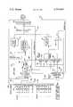
- the FIGUREis a block diagram of a microcode memory according to the present invention.
- the present inventionconsists of a microcode control memory system 10 in which a first microcode memory 12 and a second microcode memory 14 contain all of the control function outputs necessary to implement the instruction inputs.
- the modifying control output fieldsare provided externally to the memory to provide the complete output function.
- the input instruction code to the systemis provided on input line 16 to an instruction code register 18.
- Register 18is connected to microcode memory 12 as well as to an output hardware translation network 20.
- Network 20is connected to group network select register 22 and determines from input address bits which of several possible inputs to register 22 will be selected for output from register 22.
- Group network select register 22is connected to a lower address register 24 associated with microcode memory 14.
- An upper address register 26provides additional input to the second microcode memory 14.
- An adder 28provides an address incrementing function when the microcode memory 14 is proceeding in serial order through a sequence of instructions.
- Outputs from microcode memories 12 and 14are connected to an output select network 30 which selects the appropriate microcode memory for output to the output register 32.
- Control state for the microcode control memoryare provided through both a single event register 34 and a group event register 35.
- the single event register 34is connected to a single event select register 36 the output of which is connected to register 24 as a control function.
- the single event network 34receives as an input a select code on a bus 38 from the output register 32 when an appropriate instruction in a sequence of instructions is reached so that the system is functionally aware that sensed events must provide output control state bits.
- a control line 40is also connected between register 35 for group events and the output register 32.
- the output of group event network 35is connected to group select network 22 as another input.
- Logic control network 42controls whether input A or input B will be selected by way of upper register 26 as the upper portion of the address supplied to microcode memory 14.
- Logic control network 42may be an OR gate as shown in the FIGURE. This network receives an input on a control line 44 from output register 32 and a control line 46 from the single event register 36 and produces an output on control line 48 connected to register 26. Similarly, control line 46 is also connected to register 24 to complete the register control process.
- the jump addressis conveyed from the output select network 30 to an input of register 26 on line 50 which divides into a first portion 52 going to register 26 and a second portion 54 going to register 24. Each portion conveys both the upper and lower portions of the jump address to be gated as input to the microcode memory 14 under various conditions.
- the address modifier which is formed as a function of the preselected eventsis taken to be 4 bits wide. This modifier is an output of group network select register 22 and an input to the lower address register 24.
- the modifierwill be used as 4 bits of the address for microcode memory 14. If the B input is not selected, then the particular 4 bits of the jump address provided on bus 50 will be used as the particular 4 bits of address to microcode memory 14.
- the gate A input on the lower address register 24is responsible for causing a replacement of the lower portion of the jump address with the modifier bits on line 56.
- the gate A input on line 46is the output of the single event register 36, which is a one-bit register, or flip flop, receiving a selected central processor event by way of the single event network 34.
- Register 36also receives a control bit from either microcode memory 12 or microcode memory 14 to allow inversion of the state of the selected central processor event, to cause the reverse control function.
- the selection of the modifieris itself actually conditioned on single central processor events.
- the modified jump addressthus becomes a conditional modified jump address.
- the upper part of the address to microcode memory 14is contained in the upper address register 26.
- the lower address register 24there are two possible inputs and a gate A control input line from network 42. In this case, however, the B input and the gate A input are different.
- the B inputis a particular 4 bits of the incremented form of the previous microcode address.
- the gate A inputis the output of the gate A function from network 42 which is an OR function between its input lines 44 and 46.
- the input on line 46 to the gate A upper network 42is the same as the gate A lower address on line 46 from network 36 so, therefore, whenever the A input is gated to the lower address register 24, the A input is also gated to the upper address register 26. When this occurs, the entire jump address will be used to load both the upper address register 26 and the lower address register 24.
- the input to network 42 on line 44is a control bit from microcode output register 32 which, when set, forces the gate A signal to the upper address register 26 to thus select the A input to the upper address register 26 but not affecting the gate A for lower address register 24.
- This situationwould arise whenever a modified address is desired in that the upper 4 bits of the address to microcode memory 14 would be forced to be the upper 4 bits of the jump address while the lower 4 bits would be the modifier based on preselected conditions provided that a gate A lower address register 24 condition has not occurred.
- a jump addressmay be used as an entire 8-bit address or it may be divided into a 4-bit jump address portion and a 4-bit modifier portion or other relevant combinations based on the principle of this invention.
- Group event network 35has, for example, eight inputs each consisting of an event group. Each of these event groups may have, for example, 4 bits each of which could form a modifier.
- a 3-bit select codeis provided from the output register 32 as a control function to the event network 36 to select one of the eight group events to be the output provided on line 58 to network 22.
- the event groupsare, in nature, dynamic central processor events or conditions which must be sensed by the microcode control circuitry so as to have the microcode memory generate the correct sequence of microcode control words for central processor control function based on the original instruction command provided on input line 16.
- the 3-bit select code on line 40is provided by either microcode memory 12 or 14 and is predetermined by the microcode program. There is a second rank of group selection handled by a group network 22 with one of its inputs being the output of group event network 36 received on line 58. Three other inputs may also be provided to group network 22 for example.
- the B and C inputsmay be selected function code bits in addition to the basic input instruction code on line 16. Because the design of the system of this example shows a microcode memory 12 having 256 words which therefore does not allow an address larger than 8 bits, any additional instruction code bits must be used as modifiers to microcode memory 14.
- one significant advantage of the present inventionis that longer instructions containing additional bits may be provided in a system having a nominal 8-bit instruction code such as for example a 12-bit instruction code in particular cases.
- the B or C inputs to group network 22are selected by way of an input control code which is an output of the hardware translation network 20.
- the hardware translation network 20will set one of its two outputs for only a small subset of a 256 possible machine language instructions provided by the 8-bit function code. This is done since only a subset of the entire machine language instruction set needs to use the additional instruction code bits to gain information about instruction execution.
- the economyresults in that rather than making the entire system responsive to 12-bit instructions only a particular subset of machine language instructions must be responsive to 12-bit instruction codes where an 8-bit instruction code is adequate for the majority of cases.
- the fourth input to group network 22is a particular 4 bits of the incremented 4 of the previous microcode address received from adder 28. Recall that the particular 4 bits were discussed earlier and were shown to be used as an input to the upper address register 26. This incremented form of the previous address will be used whenever it is desired to cycle sequentially through microcode addresses.
- conditional modified jump mechanismwill be explained using additional special terms to refer to some of the essential control signals from microcode by a 3-letter mnemonic. Therefore:
- PSAThis is a 4-bit select code to choose one of sixteen possible single events from the central processor to be used as a condition for conditional jumps and conditional modified jumps and is an input to group event network 36.
- PSBThis is a 3-bit select code to choose one of eight groups (each 4 bits) to be used as an address modifier and is an input to group event address network 22.
- PSCThis uses two control lines to choose either the A or D inputs to group event address network 22.
- MO1This is the jump address from microcode which specifies the next location to be referenced in microcode if a non-modified jump occurs. Also, if a modified jump does occur, then the upper 4 bits of this field (register 36, groups 4, 5, 6 and 7) are used as the upper 4 bits of the next microcode address with the lower 4 bits being the modifier.
- the microcode fields necessary for a conditional modified branch operationare shown.
- the PSA and NOT fieldmust pass through both the output register 32 and the event register 36, whereas the MO1 field does not pass through any registers prior to reaching the lower address register 24, the PSA and NOT are set in address 81 and the MO1 field is set in address 83.
- microcode memory 14A modified jump operation occurring from microcode memory 12 to memory 14 will be described. Assuming microcode memory 12 is being selected at the output select 30 and that a condition occurs which will cause switching to memory 14, examine what occurs if the op-code at input line 16 is a 32 code. By definition, a 32 code is one which, when seen by the hardware translation network 20, will cause the select B control input at group event network 22 to be set. This will enable additional selected op-code bits to be gated into group network 22 via the B input, thus causing these additional op-code bits to be the modifier.
- hardware translation network 20rather than microcode control bits are responsible for establishing a modifier.
Landscapes
- Engineering & Computer Science (AREA)
- Software Systems (AREA)
- Theoretical Computer Science (AREA)
- Physics & Mathematics (AREA)
- General Engineering & Computer Science (AREA)
- General Physics & Mathematics (AREA)
- Executing Machine-Instructions (AREA)
Abstract
Description
______________________________________ Microcode Address Microcode Memory 1 Fields ______________________________________ 81 PSA=1,NOT=0 82 PSB=3,PSC=2,MOD=1 83 MO1=90 84 . . . . . . . . 90 16 word table which is 91 entered if the conditional 92 modified branch does occur. . Which word is referenced . is dependent upon what . value the modifier . has. 9F ______________________________________
Claims (7)
Priority Applications (3)
| Application Number | Priority Date | Filing Date | Title |
|---|---|---|---|
| US06/077,955US4336602A (en) | 1979-09-24 | 1979-09-24 | Network for generating modified microcode addresses |
| AU61934/80AAU535105B2 (en) | 1979-09-24 | 1980-09-01 | Network for generating modified microcode addresses |
| CA000359552ACA1137642A (en) | 1979-09-24 | 1980-09-04 | Network for generating modified microcode addresses |
Applications Claiming Priority (1)
| Application Number | Priority Date | Filing Date | Title |
|---|---|---|---|
| US06/077,955US4336602A (en) | 1979-09-24 | 1979-09-24 | Network for generating modified microcode addresses |
Publications (1)
| Publication Number | Publication Date |
|---|---|
| US4336602Atrue US4336602A (en) | 1982-06-22 |
Family
ID=22141001
Family Applications (1)
| Application Number | Title | Priority Date | Filing Date |
|---|---|---|---|
| US06/077,955Expired - LifetimeUS4336602A (en) | 1979-09-24 | 1979-09-24 | Network for generating modified microcode addresses |
Country Status (3)
| Country | Link |
|---|---|
| US (1) | US4336602A (en) |
| AU (1) | AU535105B2 (en) |
| CA (1) | CA1137642A (en) |
Cited By (6)
| Publication number | Priority date | Publication date | Assignee | Title |
|---|---|---|---|---|
| US4864535A (en)* | 1985-12-06 | 1989-09-05 | Texas Instruments Incorporated | Entry point address circuit for microcode rom |
| US4879678A (en)* | 1984-03-26 | 1989-11-07 | Hitachi, Ltd. | Programmable sequence controller with operation codes partially supplying jump to addresses of machine language instruction |
| US5594880A (en)* | 1992-02-14 | 1997-01-14 | Motorola Inc. | System for executing a plurality of tasks within an instruction in different orders depending upon a conditional value |
| US6038659A (en)* | 1997-11-12 | 2000-03-14 | International Business Machines Corporation | Method for using read-only memory to generate controls for microprocessor |
| US6253305B1 (en)* | 1995-05-31 | 2001-06-26 | Matsushita Electric Industrial Co., Ltd. | Microprocessor for supporting reduction of program codes in size |
| US9342303B2 (en) | 2013-03-15 | 2016-05-17 | Intel Corporation | Modified execution using context sensitive auxiliary code |
Families Citing this family (1)
| Publication number | Priority date | Publication date | Assignee | Title |
|---|---|---|---|---|
| EP0215028A4 (en)* | 1985-02-20 | 1987-07-23 | Magellan Corp Australia | Microprogram controller. |
Citations (10)
| Publication number | Priority date | Publication date | Assignee | Title |
|---|---|---|---|---|
| US3634883A (en)* | 1969-11-12 | 1972-01-11 | Honeywell Inc | Microinstruction address modification and branch system |
| US3766532A (en)* | 1972-04-28 | 1973-10-16 | Nanodata Corp | Data processing system having two levels of program control |
| US3839705A (en)* | 1972-12-14 | 1974-10-01 | Gen Electric | Data processor including microprogram control means |
| US3930236A (en)* | 1973-06-05 | 1975-12-30 | Burroughs Corp | Small micro program data processing system employing multi-syllable micro instructions |
| US4027291A (en)* | 1974-09-12 | 1977-05-31 | Fujitsu Ltd. | Access control unit |
| US4100601A (en)* | 1975-12-24 | 1978-07-11 | Computer Automation, Inc. | Multiplexer for a distributed input/out controller system |
| US4124888A (en)* | 1975-12-24 | 1978-11-07 | Computer Automation, Inc. | Peripheral-unit controller apparatus |
| US4124893A (en)* | 1976-10-18 | 1978-11-07 | Honeywell Information Systems Inc. | Microword address branching bit arrangement |
| US4151597A (en)* | 1976-07-23 | 1979-04-24 | Thomson-Csf | Microprogrammable control unit |
| US4168523A (en)* | 1975-11-07 | 1979-09-18 | Ncr Corporation | Data processor utilizing a two level microaddressing controller |
- 1979
- 1979-09-24USUS06/077,955patent/US4336602A/ennot_activeExpired - Lifetime
- 1980
- 1980-09-01AUAU61934/80Apatent/AU535105B2/ennot_activeCeased
- 1980-09-04CACA000359552Apatent/CA1137642A/ennot_activeExpired
Patent Citations (10)
| Publication number | Priority date | Publication date | Assignee | Title |
|---|---|---|---|---|
| US3634883A (en)* | 1969-11-12 | 1972-01-11 | Honeywell Inc | Microinstruction address modification and branch system |
| US3766532A (en)* | 1972-04-28 | 1973-10-16 | Nanodata Corp | Data processing system having two levels of program control |
| US3839705A (en)* | 1972-12-14 | 1974-10-01 | Gen Electric | Data processor including microprogram control means |
| US3930236A (en)* | 1973-06-05 | 1975-12-30 | Burroughs Corp | Small micro program data processing system employing multi-syllable micro instructions |
| US4027291A (en)* | 1974-09-12 | 1977-05-31 | Fujitsu Ltd. | Access control unit |
| US4168523A (en)* | 1975-11-07 | 1979-09-18 | Ncr Corporation | Data processor utilizing a two level microaddressing controller |
| US4100601A (en)* | 1975-12-24 | 1978-07-11 | Computer Automation, Inc. | Multiplexer for a distributed input/out controller system |
| US4124888A (en)* | 1975-12-24 | 1978-11-07 | Computer Automation, Inc. | Peripheral-unit controller apparatus |
| US4151597A (en)* | 1976-07-23 | 1979-04-24 | Thomson-Csf | Microprogrammable control unit |
| US4124893A (en)* | 1976-10-18 | 1978-11-07 | Honeywell Information Systems Inc. | Microword address branching bit arrangement |
Cited By (6)
| Publication number | Priority date | Publication date | Assignee | Title |
|---|---|---|---|---|
| US4879678A (en)* | 1984-03-26 | 1989-11-07 | Hitachi, Ltd. | Programmable sequence controller with operation codes partially supplying jump to addresses of machine language instruction |
| US4864535A (en)* | 1985-12-06 | 1989-09-05 | Texas Instruments Incorporated | Entry point address circuit for microcode rom |
| US5594880A (en)* | 1992-02-14 | 1997-01-14 | Motorola Inc. | System for executing a plurality of tasks within an instruction in different orders depending upon a conditional value |
| US6253305B1 (en)* | 1995-05-31 | 2001-06-26 | Matsushita Electric Industrial Co., Ltd. | Microprocessor for supporting reduction of program codes in size |
| US6038659A (en)* | 1997-11-12 | 2000-03-14 | International Business Machines Corporation | Method for using read-only memory to generate controls for microprocessor |
| US9342303B2 (en) | 2013-03-15 | 2016-05-17 | Intel Corporation | Modified execution using context sensitive auxiliary code |
Also Published As
| Publication number | Publication date |
|---|---|
| AU535105B2 (en) | 1984-03-01 |
| AU6193480A (en) | 1981-04-02 |
| CA1137642A (en) | 1982-12-14 |
Similar Documents
| Publication | Publication Date | Title |
|---|---|---|
| US4984151A (en) | Flexible, next-address generation microprogram sequencer | |
| US4502115A (en) | Data processing unit of a microprogram control system for variable length data | |
| US4179731A (en) | Microprogrammed control system | |
| US5093783A (en) | Microcomputer register bank accessing | |
| EP0377976A2 (en) | Microcode control apparatus utilizing programmable logic array circuits | |
| US4459666A (en) | Plural microcode control memory | |
| US4691278A (en) | Data processor executing microprograms according to a plurality of system architectures | |
| US5964861A (en) | Method for writing a program to control processors using any instructions selected from original instructions and defining the instructions used as a new instruction set | |
| US4285039A (en) | Memory array selection mechanism | |
| KR980004059A (en) | Data processing apparatus and register address conversion method | |
| US5410658A (en) | Microprocessor for carrying out a plurality of different microprograms at the same time and method for controlling the microprocessor | |
| US4336602A (en) | Network for generating modified microcode addresses | |
| US5032983A (en) | Entry point mapping and skipping method and apparatus | |
| US5046040A (en) | Microprogram control apparatus using don't care bits as part of address bits for common instructions and generating variable control bits | |
| US4394735A (en) | Data processor controlled by microprograms | |
| US4126896A (en) | Microprogrammed large-scale integration (LSI) microprocessor | |
| US4674063A (en) | Information processing apparatus having a sequence control function | |
| EP0163279B1 (en) | Vector processor | |
| US4493029A (en) | Microprocessor with PLA adapted to implement subroutines | |
| US5124910A (en) | Microprogram control apparatus for generating a branch condition signal to be designated by a micro-branch instruction | |
| US5479620A (en) | Control unit modifying micro instructions for one cycle execution | |
| US5426766A (en) | Microprocessor which holds selected data for continuous operation | |
| US4337510A (en) | Read control system for a control storage device | |
| US4831572A (en) | Polynomial vector arithmetic operation control system | |
| US4675843A (en) | Programmable logic controller |
Legal Events
| Date | Code | Title | Description |
|---|---|---|---|
| STCF | Information on status: patent grant | Free format text:PATENTED CASE | |
| AS | Assignment | Owner name:CERIDIAN CORPORATION, MINNESOTA Free format text:CHANGE OF NAME;ASSIGNOR:CONTROL DATA CORPORATION;REEL/FRAME:008829/0610 Effective date:19920731 Owner name:CONTROL DATA SYSTEMS, INC., MINNESOTA Free format text:ASSIGNMENT OF ASSIGNORS INTEREST;ASSIGNOR:CERIDIAN CORPORATION;REEL/FRAME:008829/0569 Effective date:19920731 | |
| AS | Assignment | Owner name:NATIONSBANK OF TEXAS, N.A., TEXAS Free format text:SECURITY AGREEMENT;ASSIGNORS:CONTROL DATA HOLDING CORPORATION;CONTROL DATA SYSTEMS, INC.;CONTROL DATA ASIA, INC.;AND OTHERS;REEL/FRAME:008989/0083 Effective date:19971126 | |
| AS | Assignment | Owner name:NATIONSBANK, N.A., NORTH CAROLINA Free format text:MERGER;ASSIGNOR:NATIONSBANK OF TEXAS, N.A.;REEL/FRAME:009405/0749 Effective date:19980506 | |
| AS | Assignment | Owner name:CONTROL DATA ASIA, INC., MINNESOTA Free format text:TERMINATION, RELEASE AND REASSIGNMENT OF SECURITY INTEREST IN CERTIAN UNITED STATES PATENTS.;ASSIGNOR:NATIONSBANK, N.A.;REEL/FRAME:009662/0347 Effective date:19980728 Owner name:CONTROL DATA INTERNATIONAL TRADING, INC., MINNESOT Free format text:TERMINATION, RELEASE AND REASSIGNMENT OF SECURITY INTEREST IN CERTIAN UNITED STATES PATENTS.;ASSIGNOR:NATIONSBANK, N.A.;REEL/FRAME:009662/0347 Effective date:19980728 Owner name:CONTROL DATA REAL ESTATE, INC., MINNESOTA Free format text:TERMINATION, RELEASE AND REASSIGNMENT OF SECURITY INTEREST IN CERTIAN UNITED STATES PATENTS.;ASSIGNOR:NATIONSBANK, N.A.;REEL/FRAME:009662/0347 Effective date:19980728 Owner name:INTER-AMERICAN CONTROL DATA CORPORATION, MINNESOTA Free format text:TERMINATION, RELEASE AND REASSIGNMENT OF SECURITY INTEREST IN CERTIAN UNITED STATES PATENTS.;ASSIGNOR:NATIONSBANK, N.A.;REEL/FRAME:009662/0347 Effective date:19980728 Owner name:MERIDIAN ENVIRONMENTAL TECHNOLOGIES, INC., MINNESO Free format text:TERMINATION, RELEASE AND REASSIGNMENT OF SECURITY INTEREST IN CERTIAN UNITED STATES PATENTS.;ASSIGNOR:NATIONSBANK, N.A.;REEL/FRAME:009662/0347 Effective date:19980728 Owner name:CONTROL DATA BELGIUM, INC., MINNESOTA Free format text:TERMINATION, RELEASE AND REASSIGNMENT OF SECURITY INTEREST IN CERTIAN UNITED STATES PATENTS.;ASSIGNOR:NATIONSBANK, N.A.;REEL/FRAME:009662/0347 Effective date:19980728 Owner name:CONTROL DATA PAN AMERICAN CORPORATION, MINNESOTA Free format text:TERMINATION, RELEASE AND REASSIGNMENT OF SECURITY INTEREST IN CERTIAN UNITED STATES PATENTS.;ASSIGNOR:NATIONSBANK, N.A.;REEL/FRAME:009662/0347 Effective date:19980728 Owner name:CONTROL DATA CHINA, INC., MINNESOTA Free format text:TERMINATION, RELEASE AND REASSIGNMENT OF SECURITY INTEREST IN CERTIAN UNITED STATES PATENTS.;ASSIGNOR:NATIONSBANK, N.A.;REEL/FRAME:009662/0347 Effective date:19980728 Owner name:CONTROL DATA INDO-ASIA COMPANY, MINNESOTA Free format text:TERMINATION, RELEASE AND REASSIGNMENT OF SECURITY INTEREST IN CERTIAN UNITED STATES PATENTS.;ASSIGNOR:NATIONSBANK, N.A.;REEL/FRAME:009662/0347 Effective date:19980728 Owner name:CONTROL INTERNATIONAL EMPLOYMENT, INC., MINNESOTA Free format text:TERMINATION, RELEASE AND REASSIGNMENT OF SECURITY INTEREST IN CERTIAN UNITED STATES PATENTS.;ASSIGNOR:NATIONSBANK, N.A.;REEL/FRAME:009662/0347 Effective date:19980728 Owner name:CONTROL DATA INDIA, NC., MINNESOTA Free format text:TERMINATION, RELEASE AND REASSIGNMENT OF SECURITY INTEREST IN CERTIAN UNITED STATES PATENTS.;ASSIGNOR:NATIONSBANK, N.A.;REEL/FRAME:009662/0347 Effective date:19980728 Owner name:CONTROL DATA FAR EAST, INC., MINNESOTA Free format text:TERMINATION, RELEASE AND REASSIGNMENT OF SECURITY INTEREST IN CERTIAN UNITED STATES PATENTS.;ASSIGNOR:NATIONSBANK, N.A.;REEL/FRAME:009662/0347 Effective date:19980728 Owner name:CONTROL DATA SYSTEMS, INC., MINNESOTA Free format text:TERMINATION, RELEASE AND REASSIGNMENT OF SECURITY INTEREST IN CERTIAN UNITED STATES PATENTS.;ASSIGNOR:NATIONSBANK, N.A.;REEL/FRAME:009662/0347 Effective date:19980728 Owner name:CONTROL DATA HOLDING CORPORATION, MINNESOTA Free format text:TERMINATION, RELEASE AND REASSIGNMENT OF SECURITY INTEREST IN CERTIAN UNITED STATES PATENTS.;ASSIGNOR:NATIONSBANK, N.A.;REEL/FRAME:009662/0347 Effective date:19980728 | |
| AS | Assignment | Owner name:CHASE MANHATTAN BANK, THE, NEW YORK Free format text:PATENT SECURITY AGREEMENT;ASSIGNOR:ALLIANT TECHSYSTEMS INC.;REEL/FRAME:009662/0089 Effective date:19981124 | |
| AS | Assignment | Owner name:LAURENCE J. MARHOEFER, VIRGINIA Free format text:ASSIGNMENT OF ASSIGNORS INTEREST;ASSIGNOR:CONTROL DATA SYSTEMS, INC.;REEL/FRAME:009737/0215 Effective date:19980728 | |
| AS | Assignment | Owner name:ALLIANT TECHSYSTEMS INC., MINNESOTA Free format text:SECURITY INTEREST;ASSIGNOR:JPMORGAN CHASE BANK (FORMERLY KNOWN AS THE CHASE MANHATTAN BANK);REEL/FRAME:015201/0351 Effective date:20040331 |