US4297162A - Plasma etching using improved electrode - Google Patents
Plasma etching using improved electrodeDownload PDFInfo
- Publication number
- US4297162A US4297162AUS06/085,564US8556479AUS4297162AUS 4297162 AUS4297162 AUS 4297162AUS 8556479 AUS8556479 AUS 8556479AUS 4297162 AUS4297162 AUS 4297162A
- Authority
- US
- United States
- Prior art keywords
- electrode
- slice
- holder
- workpiece surface
- chamber
- Prior art date
- Legal status (The legal status is an assumption and is not a legal conclusion. Google has not performed a legal analysis and makes no representation as to the accuracy of the status listed.)
- Expired - Lifetime
Links
Images

Classifications
- H—ELECTRICITY
- H01—ELECTRIC ELEMENTS
- H01J—ELECTRIC DISCHARGE TUBES OR DISCHARGE LAMPS
- H01J37/00—Discharge tubes with provision for introducing objects or material to be exposed to the discharge, e.g. for the purpose of examination or processing thereof
- H01J37/32—Gas-filled discharge tubes
- H01J37/32431—Constructional details of the reactor
- H01J37/32623—Mechanical discharge control means
- C—CHEMISTRY; METALLURGY
- C23—COATING METALLIC MATERIAL; COATING MATERIAL WITH METALLIC MATERIAL; CHEMICAL SURFACE TREATMENT; DIFFUSION TREATMENT OF METALLIC MATERIAL; COATING BY VACUUM EVAPORATION, BY SPUTTERING, BY ION IMPLANTATION OR BY CHEMICAL VAPOUR DEPOSITION, IN GENERAL; INHIBITING CORROSION OF METALLIC MATERIAL OR INCRUSTATION IN GENERAL
- C23F—NON-MECHANICAL REMOVAL OF METALLIC MATERIAL FROM SURFACE; INHIBITING CORROSION OF METALLIC MATERIAL OR INCRUSTATION IN GENERAL; MULTI-STEP PROCESSES FOR SURFACE TREATMENT OF METALLIC MATERIAL INVOLVING AT LEAST ONE PROCESS PROVIDED FOR IN CLASS C23 AND AT LEAST ONE PROCESS COVERED BY SUBCLASS C21D OR C22F OR CLASS C25
- C23F4/00—Processes for removing metallic material from surfaces, not provided for in group C23F1/00 or C23F3/00
- H—ELECTRICITY
- H01—ELECTRIC ELEMENTS
- H01J—ELECTRIC DISCHARGE TUBES OR DISCHARGE LAMPS
- H01J37/00—Discharge tubes with provision for introducing objects or material to be exposed to the discharge, e.g. for the purpose of examination or processing thereof
- H01J37/32—Gas-filled discharge tubes
- H01J37/32431—Constructional details of the reactor
- H01J37/3244—Gas supply means
- H—ELECTRICITY
- H01—ELECTRIC ELEMENTS
- H01J—ELECTRIC DISCHARGE TUBES OR DISCHARGE LAMPS
- H01J37/00—Discharge tubes with provision for introducing objects or material to be exposed to the discharge, e.g. for the purpose of examination or processing thereof
- H01J37/32—Gas-filled discharge tubes
- H01J37/32431—Constructional details of the reactor
- H01J37/32532—Electrodes
- H01J37/32541—Shape
- H—ELECTRICITY
- H05—ELECTRIC TECHNIQUES NOT OTHERWISE PROVIDED FOR
- H05H—PLASMA TECHNIQUE; PRODUCTION OF ACCELERATED ELECTRICALLY-CHARGED PARTICLES OR OF NEUTRONS; PRODUCTION OR ACCELERATION OF NEUTRAL MOLECULAR OR ATOMIC BEAMS
- H05H1/00—Generating plasma; Handling plasma
- H05H1/24—Generating plasma
- H05H1/26—Plasma torches
- H05H1/32—Plasma torches using an arc
- H05H1/34—Details, e.g. electrodes, nozzles
- H05H1/40—Details, e.g. electrodes, nozzles using applied magnetic fields, e.g. for focusing or rotating the arc
- Y—GENERAL TAGGING OF NEW TECHNOLOGICAL DEVELOPMENTS; GENERAL TAGGING OF CROSS-SECTIONAL TECHNOLOGIES SPANNING OVER SEVERAL SECTIONS OF THE IPC; TECHNICAL SUBJECTS COVERED BY FORMER USPC CROSS-REFERENCE ART COLLECTIONS [XRACs] AND DIGESTS
- Y10—TECHNICAL SUBJECTS COVERED BY FORMER USPC
- Y10S—TECHNICAL SUBJECTS COVERED BY FORMER USPC CROSS-REFERENCE ART COLLECTIONS [XRACs] AND DIGESTS
- Y10S422/00—Chemical apparatus and process disinfecting, deodorizing, preserving, or sterilizing
- Y10S422/906—Plasma or ion generation means
Definitions
- This inventionrelates to manufacture of semiconductor devices or the like, and more particularly to a radio frequency plasma reactor.
- radio frequency plasma etching of conductive coatings on semiconductor slicesis improved by the use of a curved electrode which is closer to the slice at the center than at the periphery.
- the electrodeis in a symmetrical chamber which contains only one slice, and reactant gases are admitted through apertures in the electrode.
- An r.f. power sourceis connected between the electrode and a holder for the slice.
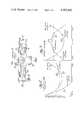
- FIG. 1is an elevation view in section of an r.f. plasma reactor system employing the features of the invention
- FIG. 2is a graphic representation of etch rate vs position on a slice in a conventional plasma reactor for various conditions of r.f. power and gas pressure;
- FIG. 3is a graphic representation of etch rate vs position on a silicon slice for various conditions of r.f. power and gas pressure when etching a polycrystalline silicon coating on the slice using the features of the invention
- FIG. 4is a plan view of an electrode in the reactor of FIG. 3;
- FIG. 5is an elevation view in section of the electrode of FIG. 4, taken along the line 5--5 in FIG. 4.
- an r.f. plasma reactor 10which may use the tapered or shaped electrode of the invention.
- the reactorincludes a chamber 11 of suitable mechanical construction which permits it to be pumped down to a high vacuum via outlet 12, yet permits ready access for installing and removing a silicon slice 13 on a conductive holder 14.
- the chamber 11is of a size just large enough to hold one silicon slice 13, rather than several as in earlier designs, because a symmetrical r.f. chamber permits better control of variables, and automatic slice handling is facilitated.
- the holder 14is electrically grounded, or connected to the return side of an r.f. source 15.
- the upper electrode 16 of the reactorhas a tapered surface 17 facing the slice 13, according to the invention.
- the electrode 16is composed of aluminum and is connected to the r.f. source 15 by a conductor passing out through the walls of the chamber 11 but insulated therefrom.
- the r.f. sourceis of standard construction and includes controls for power level, loading, tuning, and the like.
- the frequency of 13.54 MHzis assigned by the FCC.
- a gas inlet 18 coupled through holes in the electrode 16is connected to multiple sources of various gases which are used in etching or treating the upper face of the slice 13 or materials thereon. For example, O 2 and CF 4 or CCl 4 are used to etch aluminum or polycrystalline silicon films deposited on a silicon slice 13, and gases such as NH 3 are used for post etch treatment.
- a temperature control and thermometerare used to maintain the temperature within the chamber at the desired level.
- the gas flow rateis of course adjusted by the inlet rate at the port 18 and the pump rate of vacuum pump connected to the outlet 12.
- a plasmais generated in the space between the holder 14 and the lower surface 17 of the electrode 16, in the presence of a high power r.f. field and the desired gas.
- the spacing between the holder 14 and the electrode 16is about 1/2 inch for etching 4 inch diameter slices 13.
- the emissions from the plasma as etching proceedsmay be monitored by a spectrophotometer aimed at this space through a port in the chamber, not shown.
- FIG. 2a plot of relative etch rate vs position along the slice for various conditions shows the very strong dependence upon power level and pressure for a reactor as seen in FIG. 1, but with a flat bottom surface 17 on the electrode 16 rather than the tapered electrode of the invention.
- the r.f. poweris varied between 50 and 300 watts, and/or the pressure within the chamber is varied between 0.5 and 3 torr.
- the oxygen flow rateis 3 cc/min and the CF 4 flow rate is 40 cc/min.
- the nominal etch rate under these conditionsis about 2000 to 4000 A/min when etching a polysilicon film deposited over SiO 2 on a silicon slice. It is noted in graph 20 that when the r.f.
- the relative etch ratewill vary as seen in FIG. 3.
- the variationis about the same as before, but for the low r.f. power or high pressure extreme the curve is reversed as seen by graph 24. That is, the curve for high power is a mirror image of that for low power because the area of plasma concentration will tend to be at the center rather than an edge. This phenomena produces a condition at intermediate r.f. power or pressure wherein the curves approximately cancel one another and a graph 25 results which is more nearly flat.
- the shape of the electrode 16is shown in more detail in FIGS. 4 and 5.
- the surface 17 in this caseis a section of a sphere with the deviation from flat being 1/2 inch for a 6 inch diameter electrode used on 4 inch slices 13.
- Other shapesare suitable; for example a conical section (with the tip 1/2 inch closer to the slice than the edges) provides excellent results, though not as flat as for a spherical section.
- a hyperbolic or elipsoid surface resembling that of FIG. 4may be found to provide perferred results.
- the holes 27 in the electrode 16are for gas inlet in a more uniform manner, although the gas inlet may be at the side or bottom of the chamber 11.
Landscapes
- Engineering & Computer Science (AREA)
- Physics & Mathematics (AREA)
- Plasma & Fusion (AREA)
- Chemical & Material Sciences (AREA)
- Analytical Chemistry (AREA)
- Spectroscopy & Molecular Physics (AREA)
- Materials Engineering (AREA)
- Mechanical Engineering (AREA)
- Metallurgy (AREA)
- Organic Chemistry (AREA)
- Drying Of Semiconductors (AREA)
Abstract
Description
This invention relates to manufacture of semiconductor devices or the like, and more particularly to a radio frequency plasma reactor.
In the manufacture of semiconductor devices, r.f. plasma processing has been favored for steps such as the etching of polysilicon or aluminum in photolithographic patterning, especially with the finer resolution needed for VLSI type devices. Also, requirements for automated handling of slices has resulted in the use of single-slice reaction chambers instead of the conventional multiple-slice batch reactors. As the line widths and material thicknesses decrease in advanced processes, the difficulties in controlling the etch uniformily across the slice become magnified. The consequences of variations in etch rate with changes in r.f. power or gas pressure become more catastrophic as the resolution becomes more stringent.
It is the principal object of this invention to provide an improved method of plasma processing of semiconductor slices. Another object is to reduce the effect of process variations in treating semiconductor slices, particularly in an r.f. plasma reactor. A further object is to provide an improved single-slice radio frequency plasma reactor.
In accordance with an embodiment of the invention, radio frequency plasma etching of conductive coatings on semiconductor slices is improved by the use of a curved electrode which is closer to the slice at the center than at the periphery. Preferably, the electrode is in a symmetrical chamber which contains only one slice, and reactant gases are admitted through apertures in the electrode. An r.f. power source is connected between the electrode and a holder for the slice.
The novel features believed characteristic of the invention are set forth in the appended claims. The invention itself, however, as well as other features and advantages thereof, will be best understood by reference to the detailed description which follows, read in conjunction with the accompanying drawings, wherein:
FIG. 1 is an elevation view in section of an r.f. plasma reactor system employing the features of the invention;
FIG. 2 is a graphic representation of etch rate vs position on a slice in a conventional plasma reactor for various conditions of r.f. power and gas pressure;
FIG. 3 is a graphic representation of etch rate vs position on a silicon slice for various conditions of r.f. power and gas pressure when etching a polycrystalline silicon coating on the slice using the features of the invention;
FIG. 4 is a plan view of an electrode in the reactor of FIG. 3; and
FIG. 5 is an elevation view in section of the electrode of FIG. 4, taken along theline 5--5 in FIG. 4.
Referring to FIG. 1, an r.f.plasma reactor 10 is shown which may use the tapered or shaped electrode of the invention. The reactor includes a chamber 11 of suitable mechanical construction which permits it to be pumped down to a high vacuum via outlet 12, yet permits ready access for installing and removing asilicon slice 13 on aconductive holder 14. Preferably, the chamber 11 is of a size just large enough to hold onesilicon slice 13, rather than several as in earlier designs, because a symmetrical r.f. chamber permits better control of variables, and automatic slice handling is facilitated. Theholder 14 is electrically grounded, or connected to the return side of an r.f.source 15. Theupper electrode 16 of the reactor has atapered surface 17 facing theslice 13, according to the invention. Theelectrode 16 is composed of aluminum and is connected to the r.f.source 15 by a conductor passing out through the walls of the chamber 11 but insulated therefrom. The r.f. source is of standard construction and includes controls for power level, loading, tuning, and the like. The frequency of 13.54 MHz is assigned by the FCC. Agas inlet 18 coupled through holes in theelectrode 16 is connected to multiple sources of various gases which are used in etching or treating the upper face of theslice 13 or materials thereon. For example, O2 and CF4 or CCl4 are used to etch aluminum or polycrystalline silicon films deposited on asilicon slice 13, and gases such as NH3 are used for post etch treatment. A temperature control and thermometer are used to maintain the temperature within the chamber at the desired level. The gas flow rate is of course adjusted by the inlet rate at theport 18 and the pump rate of vacuum pump connected to the outlet 12. When operating, a plasma is generated in the space between theholder 14 and thelower surface 17 of theelectrode 16, in the presence of a high power r.f. field and the desired gas. The spacing between theholder 14 and theelectrode 16 is about 1/2 inch for etching 4inch diameter slices 13. The emissions from the plasma as etching proceeds may be monitored by a spectrophotometer aimed at this space through a port in the chamber, not shown.
In FIG. 2, a plot of relative etch rate vs position along the slice for various conditions shows the very strong dependence upon power level and pressure for a reactor as seen in FIG. 1, but with aflat bottom surface 17 on theelectrode 16 rather than the tapered electrode of the invention. The r.f. power is varied between 50 and 300 watts, and/or the pressure within the chamber is varied between 0.5 and 3 torr. The oxygen flow rate is 3 cc/min and the CF4 flow rate is 40 cc/min. The nominal etch rate under these conditions is about 2000 to 4000 A/min when etching a polysilicon film deposited over SiO2 on a silicon slice. It is noted ingraph 20 that when the r.f. power is high or the pressure low (vacuum pump rate higher) the relative etch rate changes by a factor of more than two between edges and center of the slice. An even worse condition exists for low r.f. power or high pressure, illustrated bygraph 21, where the etch rate goes to zero as the plasma collapses at the center and is extremely high at the one edge where the plasma concentrates. Either of these conditions is of course unacceptable for production of high quality semiconductor devices with fine line resolution at reasonable yields. At intermediate r.f. power and pressure, a reasonably shallow deviation in the etch rate is shown by graph 22; even this, however, is not consistent with production requirements because the deviation is perhaps 15 to 20%.
Using a tapered or shaped electrode according to the invention, with the conditions otherwise the same as in FIG. 2, the relative etch rate will vary as seen in FIG. 3. At the high r.f. power or low pressure extreme seen bygraph 23, the variation is about the same as before, but for the low r.f. power or high pressure extreme the curve is reversed as seen bygraph 24. That is, the curve for high power is a mirror image of that for low power because the area of plasma concentration will tend to be at the center rather than an edge. This phenomena produces a condition at intermediate r.f. power or pressure wherein the curves approximately cancel one another and agraph 25 results which is more nearly flat.
The shape of theelectrode 16 is shown in more detail in FIGS. 4 and 5. Thesurface 17 in this case is a section of a sphere with the deviation from flat being 1/2 inch for a 6 inch diameter electrode used on 4 inch slices 13. Other shapes are suitable; for example a conical section (with the tip 1/2 inch closer to the slice than the edges) provides excellent results, though not as flat as for a spherical section. A hyperbolic or elipsoid surface resembling that of FIG. 4 may be found to provide perferred results. The holes 27 in theelectrode 16 are for gas inlet in a more uniform manner, although the gas inlet may be at the side or bottom of the chamber 11.
While this invention has been described with reference to an illustrative embodiment, this description is not intended to be construed in a limiting sense. Various modifications of the illustrative embodiment, as well as other embodiments of the invention, will be apparent to persons skilled in the art upon reference to this description. It is therefore contemplated that the appended claims will cover any such modifications or embodiments as fall within the true scope of the invention.
Claims (14)
1. A radio frequency plasma reactor electrode for treating a relatively flat workpiece surface comprising an electrode surface generally of the same size or greater in size than the workpiece surface, the electrode surface positioned facing said workpiece surface but spaced therefrom to provide a plasma zone, the electrode surface being convex shaped to include a protruding portion which is generally symmetrical about a central area of said workpiece surface and closer to said central area than to peripheral areas of said workpiece surface.
2. Apparatus according to claim 1 wherein the workpiece surface is a semiconductor slice having coatings thereon.
3. Apparatus according to claim 1 wherein said electrode surface is a section of a sphere.
4. Apparatus according to claim 3 wherein said electrode is generally circular in shape.
5. Apparatus according to claim 4 wherein the distance which the protruding portion extends toward said central area is about the same as the minimum spacing between the electrode and the workpiece surface.
6. Apparatus according to claim 5 wherein the workpiece surface is a generally round semiconductor slice having a coating thereon, and the plasma etches said coating.
7. A radio frequency plasma reactor for etching conductive coatings on semiconductor slices comprising a relatively flat conductive holder for receiving a semiconductor slice, a conductive electrode having a surface facing said holder, means for applying radio frequency voltage across the electrode and the holder to produce a plasma reaction in a space between the electrode and holder, the electrode including a central portion extending closer to the holder at about the center thereof than around the periphery thereof.
8. Apparatus according to claim 7 wherein the electrode has a curved curvex surface facing the holder.
9. Apparatus according to claim 8 wherein the curvex surface is approximately a section of a sphere.
10. Apparatus according to claim 9 wherein the conductive electrode and the holder are generally circular in shape.
11. Apparatus according to claim 10 wherein the electrode has a plurality of small apertures for inlet of reaction gases.
12. A method of etching a coating on a generally circular silicon slice comprising
(a) positioning the slice symmetrically in a chamber on a conductive holder,
(b) positioning an electrode facing the slice in the chamber, the electrode being of generally symmetrical shape with respect to the slice and having a central part closer to the slice than peripheral parts,
(c) admitting reaction gas to the chamber while vacuum-pumping the chamber,
(d) applying radio frequency voltage between the holder and the electrode.
13. A method according to claim 12 wherein said central part is shaped in a convex manner generally symmetrical with respect to the slice.
14. A method according to claim 13 wherein said reaction gas is admitted through ports in said electrode.
Priority Applications (4)
| Application Number | Priority Date | Filing Date | Title |
|---|---|---|---|
| US06/085,564US4297162A (en) | 1979-10-17 | 1979-10-17 | Plasma etching using improved electrode |
| DE8080105943TDE3069300D1 (en) | 1979-10-17 | 1980-10-01 | Apparatus for radio frequency plasma etching provided with an improved electrode and method of etching using such an apparatus |
| EP80105943AEP0027578B1 (en) | 1979-10-17 | 1980-10-01 | Apparatus for radio frequency plasma etching provided with an improved electrode and method of etching using such an apparatus |
| JP14504080AJPS5666041A (en) | 1979-10-17 | 1980-10-16 | Etching method and high frequency plasma reactor |
Applications Claiming Priority (1)
| Application Number | Priority Date | Filing Date | Title |
|---|---|---|---|
| US06/085,564US4297162A (en) | 1979-10-17 | 1979-10-17 | Plasma etching using improved electrode |
Publications (1)
| Publication Number | Publication Date |
|---|---|
| US4297162Atrue US4297162A (en) | 1981-10-27 |
Family
ID=22192473
Family Applications (1)
| Application Number | Title | Priority Date | Filing Date |
|---|---|---|---|
| US06/085,564Expired - LifetimeUS4297162A (en) | 1979-10-17 | 1979-10-17 | Plasma etching using improved electrode |
Country Status (4)
| Country | Link |
|---|---|
| US (1) | US4297162A (en) |
| EP (1) | EP0027578B1 (en) |
| JP (1) | JPS5666041A (en) |
| DE (1) | DE3069300D1 (en) |
Cited By (65)
| Publication number | Priority date | Publication date | Assignee | Title |
|---|---|---|---|---|
| US4340462A (en)* | 1981-02-13 | 1982-07-20 | Lam Research Corporation | Adjustable electrode plasma processing chamber |
| DE3241391A1 (en)* | 1981-11-12 | 1983-05-19 | Varian Associates, Inc., 94303 Palo Alto, Calif. | HIGH-FREQUENCY ETCHING TABLE WITH ELECTRICALLY TENSIONED MOUNTING PART |
| US4384938A (en)* | 1982-05-03 | 1983-05-24 | International Business Machines Corporation | Reactive ion etching chamber |
| US4426274A (en) | 1981-06-02 | 1984-01-17 | International Business Machines Corporation | Reactive ion etching apparatus with interlaced perforated anode |
| FR2532218A1 (en)* | 1982-09-01 | 1984-03-02 | Westinghouse Electric Corp | APPARATUS AND METHOD FOR LASER MACHINING IN NON-REACTIVE ATMOSPHERE |
| US4512841A (en)* | 1984-04-02 | 1985-04-23 | International Business Machines Corporation | RF Coupling techniques |
| US4534816A (en)* | 1984-06-22 | 1985-08-13 | International Business Machines Corporation | Single wafer plasma etch reactor |
| US4578559A (en)* | 1982-03-10 | 1986-03-25 | Tokyo Ohka Kogyo Co., Ltd. | Plasma etching method |
| US4585920A (en)* | 1982-05-21 | 1986-04-29 | Tegal Corporation | Plasma reactor removable insert |
| US4595484A (en)* | 1985-12-02 | 1986-06-17 | International Business Machines Corporation | Reactive ion etching apparatus |
| US4600464A (en)* | 1985-05-01 | 1986-07-15 | International Business Machines Corporation | Plasma etching reactor with reduced plasma potential |
| US4601807A (en)* | 1985-01-17 | 1986-07-22 | International Business Machines Corporation | Reactor for plasma desmear of high aspect ratio hole |
| US4612432A (en)* | 1984-09-14 | 1986-09-16 | Monolithic Memories, Inc. | Etching plasma generator diffusor and cap |
| DE3635647A1 (en)* | 1985-11-04 | 1987-05-07 | Voest Alpine Ag | Plasma reactor for etching printed circuit boards or the like |
| US4810322A (en)* | 1986-11-03 | 1989-03-07 | International Business Machines Corporation | Anode plate for a parallel-plate reactive ion etching reactor |
| US4842828A (en)* | 1987-02-18 | 1989-06-27 | Hitachi, Ltd. | Apparatus for treating surface of object with ultraviolet rays and reaction gas |
| US5061359A (en)* | 1985-01-17 | 1991-10-29 | International Business Machines Corporation | Plasma processing apparatus including three bus structures |
| DE4011933C1 (en)* | 1990-04-12 | 1991-11-28 | Balzers Ag, Balzers, Li | |
| US5087341A (en)* | 1984-03-23 | 1992-02-11 | Anelva Corporation | Dry etching apparatus and method |
| US5226967A (en)* | 1992-05-14 | 1993-07-13 | Lam Research Corporation | Plasma apparatus including dielectric window for inducing a uniform electric field in a plasma chamber |
| US5324411A (en)* | 1991-09-20 | 1994-06-28 | Toshiba Ceramics Co., Ltd. | Electrode plate for plasma etching |
| US5346601A (en)* | 1993-05-11 | 1994-09-13 | Andrew Barada | Sputter coating collimator with integral reactive gas distribution |
| US5423936A (en)* | 1992-10-19 | 1995-06-13 | Hitachi, Ltd. | Plasma etching system |
| US5439524A (en)* | 1993-04-05 | 1995-08-08 | Vlsi Technology, Inc. | Plasma processing apparatus |
| US5549780A (en)* | 1990-10-23 | 1996-08-27 | Semiconductor Energy Laboratory Co., Ltd. | Method for plasma processing and apparatus for plasma processing |
| US5558843A (en)* | 1994-09-01 | 1996-09-24 | Eastman Kodak Company | Near atmospheric pressure treatment of polymers using helium discharges |
| US5591301A (en)* | 1994-12-22 | 1997-01-07 | Siemens Aktiengesellschaft | Plasma etching method |
| US5628869A (en)* | 1994-05-09 | 1997-05-13 | Lsi Logic Corporation | Plasma enhanced chemical vapor reactor with shaped electrodes |
| US5639334A (en)* | 1995-03-07 | 1997-06-17 | International Business Machines Corporation | Uniform gas flow arrangements |
| US5698168A (en)* | 1995-11-01 | 1997-12-16 | Chorus Corporation | Unibody gas plasma source technology |
| US5711849A (en)* | 1995-05-03 | 1998-01-27 | Daniel L. Flamm | Process optimization in gas phase dry etching |
| US5716485A (en)* | 1995-06-07 | 1998-02-10 | Varian Associates, Inc. | Electrode designs for controlling uniformity profiles in plasma processing reactors |
| US5990016A (en)* | 1996-12-24 | 1999-11-23 | Samsung Electronics Co., Ltd. | Dry etching method and apparatus for manufacturing a semiconductor device |
| US5997686A (en)* | 1992-07-27 | 1999-12-07 | Tokyo Electron Limited | Process for setting a working rate distribution in an etching or plasma CVD apparatus |
| WO2001003163A1 (en)* | 1999-06-30 | 2001-01-11 | Lam Research Corporation | Gas distribution apparatus for semiconductor processing |
| US6245192B1 (en) | 1999-06-30 | 2001-06-12 | Lam Research Corporation | Gas distribution apparatus for semiconductor processing |
| US6451157B1 (en) | 1999-09-23 | 2002-09-17 | Lam Research Corporation | Gas distribution apparatus for semiconductor processing |
| US20020187647A1 (en)* | 2000-10-13 | 2002-12-12 | Rajinder Dhindsa | Stepped upper electrode for plasma processing uniformity |
| US20030094135A1 (en)* | 1999-12-24 | 2003-05-22 | Taro Komiya | Baffle plate, apparatus for producing the same, method of producing the same, and gas processing apparatus containing baffle plate |
| WO2003064725A1 (en)* | 2002-01-25 | 2003-08-07 | Applied Materials, Inc. | Gas distribution showerhead |
| US20040060514A1 (en)* | 2002-01-25 | 2004-04-01 | Applied Materials, Inc. A Delaware Corporation | Gas distribution showerhead |
| US20040074609A1 (en)* | 2002-05-23 | 2004-04-22 | Andreas Fischer | Multi-part electrode for a semiconductor processing plasma reactor and method of replacing a portion of a multi-part electrode |
| US20050011447A1 (en)* | 2003-07-14 | 2005-01-20 | Tokyo Electron Limited | Method and apparatus for delivering process gas to a process chamber |
| US20050022934A1 (en)* | 2003-07-29 | 2005-02-03 | Samsung Electronics Co., Ltd. | Plasma etching apparatus |
| FR2884044A1 (en)* | 2005-04-01 | 2006-10-06 | St Microelectronics Sa | Reactor for the deposition of an oxide layer on a platelet, notably for the deposition of tantalum pentoxide during the fabrication of integrated circuits |
| US20060260749A1 (en)* | 2005-05-20 | 2006-11-23 | Satoshi Ueda | Substrate processing apparatus and substrate processing method |
| US20070084407A1 (en)* | 2005-10-14 | 2007-04-19 | Hon Hai Precision Industry Co., Ltd. | Apparatus and method for manufacturing carbon nanotubes |
| US20080184934A1 (en)* | 1999-08-10 | 2008-08-07 | Jacques Schmitt | Plasma reactor for the treatment of large size substrates |
| US7431967B2 (en) | 2002-09-19 | 2008-10-07 | Applied Materials, Inc. | Limited thermal budget formation of PMD layers |
| US20080276958A1 (en)* | 2007-05-08 | 2008-11-13 | Applied Materials, Inc. | Substrate cleaning chamber and cleaning and conditioning methods |
| US7456116B2 (en) | 2002-09-19 | 2008-11-25 | Applied Materials, Inc. | Gap-fill depositions in the formation of silicon containing dielectric materials |
| US7552521B2 (en) | 2004-12-08 | 2009-06-30 | Tokyo Electron Limited | Method and apparatus for improved baffle plate |
| US7601242B2 (en) | 2005-01-11 | 2009-10-13 | Tokyo Electron Limited | Plasma processing system and baffle assembly for use in plasma processing system |
| US20090261066A1 (en)* | 2006-09-08 | 2009-10-22 | Ulvac, Inc | Apparatus and method for dry etching |
| US7642171B2 (en) | 2004-08-04 | 2010-01-05 | Applied Materials, Inc. | Multi-step anneal of thin films for film densification and improved gap-fill |
| US7674727B2 (en) | 2002-09-19 | 2010-03-09 | Applied Materials, Inc. | Nitrous oxide anneal of TEOS/ozone CVD for improved gapfill |
| USRE41266E1 (en) | 1990-09-18 | 2010-04-27 | Lam Research Corporation | Composite electrode for plasma processes |
| US20120097331A1 (en)* | 2008-03-20 | 2012-04-26 | Novellus Systems, Inc. | Gas flow distribution receptacles, plasma generator systems, and methods for performing plasma stripping processes |
| US20120118234A1 (en)* | 2006-07-05 | 2012-05-17 | Sumitomo Electric Industries, Ltd. | Metal organic chemical vapor deposition equipment |
| US9018108B2 (en) | 2013-01-25 | 2015-04-28 | Applied Materials, Inc. | Low shrinkage dielectric films |
| US20150118859A1 (en)* | 2013-10-24 | 2015-04-30 | Tokyo Electron Limited | Plasma processing method and plasma processing apparatus |
| US9591738B2 (en) | 2008-04-03 | 2017-03-07 | Novellus Systems, Inc. | Plasma generator systems and methods of forming plasma |
| CN110416048A (en)* | 2018-04-27 | 2019-11-05 | 北京北方华创微电子装备有限公司 | A kind of reaction chamber and semiconductor processing equipment |
| CN113549901A (en)* | 2020-04-24 | 2021-10-26 | 三星显示有限公司 | Plasma processing device |
| US20230044064A1 (en)* | 2020-01-06 | 2023-02-09 | Lam Research Corporation | Showerhead with faceplate having internal contours |
Families Citing this family (6)
| Publication number | Priority date | Publication date | Assignee | Title |
|---|---|---|---|---|
| US4342901A (en)* | 1980-08-11 | 1982-08-03 | Eaton Corporation | Plasma etching electrode |
| JPS6077427A (en)* | 1983-10-04 | 1985-05-02 | Seiko Epson Corp | dry etching equipment |
| GB8431422D0 (en)* | 1984-12-13 | 1985-01-23 | Standard Telephones Cables Ltd | Plasma reactor vessel |
| DE3914065A1 (en)* | 1989-04-28 | 1990-10-31 | Leybold Ag | DEVICE FOR CARRYING OUT PLASMA ETCHING PROCESSES |
| US5269847A (en)* | 1990-08-23 | 1993-12-14 | Applied Materials, Inc. | Variable rate distribution gas flow reaction chamber |
| US5134963A (en)* | 1991-10-28 | 1992-08-04 | International Business Machines Corporation | LPCVD reactor for high efficiency, high uniformity deposition |
Citations (3)
| Publication number | Priority date | Publication date | Assignee | Title |
|---|---|---|---|---|
| US4126530A (en)* | 1977-08-04 | 1978-11-21 | Telic Corporation | Method and apparatus for sputter cleaning and bias sputtering |
| US4172021A (en)* | 1978-10-13 | 1979-10-23 | Western Electric Company, Inc. | Method and glow-suppression devices for transporting a gas across a voltage drop |
| US4209357A (en)* | 1979-05-18 | 1980-06-24 | Tegal Corporation | Plasma reactor apparatus |
Family Cites Families (2)
| Publication number | Priority date | Publication date | Assignee | Title |
|---|---|---|---|---|
| US3879597A (en)* | 1974-08-16 | 1975-04-22 | Int Plasma Corp | Plasma etching device and process |
| US4230515A (en)* | 1978-07-27 | 1980-10-28 | Davis & Wilder, Inc. | Plasma etching apparatus |
- 1979
- 1979-10-17USUS06/085,564patent/US4297162A/ennot_activeExpired - Lifetime
- 1980
- 1980-10-01DEDE8080105943Tpatent/DE3069300D1/ennot_activeExpired
- 1980-10-01EPEP80105943Apatent/EP0027578B1/ennot_activeExpired
- 1980-10-16JPJP14504080Apatent/JPS5666041A/enactivePending
Patent Citations (3)
| Publication number | Priority date | Publication date | Assignee | Title |
|---|---|---|---|---|
| US4126530A (en)* | 1977-08-04 | 1978-11-21 | Telic Corporation | Method and apparatus for sputter cleaning and bias sputtering |
| US4172021A (en)* | 1978-10-13 | 1979-10-23 | Western Electric Company, Inc. | Method and glow-suppression devices for transporting a gas across a voltage drop |
| US4209357A (en)* | 1979-05-18 | 1980-06-24 | Tegal Corporation | Plasma reactor apparatus |
Cited By (89)
| Publication number | Priority date | Publication date | Assignee | Title |
|---|---|---|---|---|
| US4340462A (en)* | 1981-02-13 | 1982-07-20 | Lam Research Corporation | Adjustable electrode plasma processing chamber |
| US4426274A (en) | 1981-06-02 | 1984-01-17 | International Business Machines Corporation | Reactive ion etching apparatus with interlaced perforated anode |
| DE3241391A1 (en)* | 1981-11-12 | 1983-05-19 | Varian Associates, Inc., 94303 Palo Alto, Calif. | HIGH-FREQUENCY ETCHING TABLE WITH ELECTRICALLY TENSIONED MOUNTING PART |
| US4578559A (en)* | 1982-03-10 | 1986-03-25 | Tokyo Ohka Kogyo Co., Ltd. | Plasma etching method |
| US4384938A (en)* | 1982-05-03 | 1983-05-24 | International Business Machines Corporation | Reactive ion etching chamber |
| US4585920A (en)* | 1982-05-21 | 1986-04-29 | Tegal Corporation | Plasma reactor removable insert |
| FR2532218A1 (en)* | 1982-09-01 | 1984-03-02 | Westinghouse Electric Corp | APPARATUS AND METHOD FOR LASER MACHINING IN NON-REACTIVE ATMOSPHERE |
| EP0102835A3 (en)* | 1982-09-01 | 1985-12-18 | Westinghouse Electric Corporation | Apparatus and method for laser machining in a non-reactive environment |
| US4492843A (en)* | 1982-09-01 | 1985-01-08 | Westinghouse Electric Corp. | Apparatus and method for laser machining in a non-reactive environment |
| US5087341A (en)* | 1984-03-23 | 1992-02-11 | Anelva Corporation | Dry etching apparatus and method |
| US4512841A (en)* | 1984-04-02 | 1985-04-23 | International Business Machines Corporation | RF Coupling techniques |
| US4534816A (en)* | 1984-06-22 | 1985-08-13 | International Business Machines Corporation | Single wafer plasma etch reactor |
| EP0165400A1 (en) | 1984-06-22 | 1985-12-27 | International Business Machines Corporation | Apparatus for plasma etching |
| US4612432A (en)* | 1984-09-14 | 1986-09-16 | Monolithic Memories, Inc. | Etching plasma generator diffusor and cap |
| US5061359A (en)* | 1985-01-17 | 1991-10-29 | International Business Machines Corporation | Plasma processing apparatus including three bus structures |
| US4601807A (en)* | 1985-01-17 | 1986-07-22 | International Business Machines Corporation | Reactor for plasma desmear of high aspect ratio hole |
| US4600464A (en)* | 1985-05-01 | 1986-07-15 | International Business Machines Corporation | Plasma etching reactor with reduced plasma potential |
| DE3635647A1 (en)* | 1985-11-04 | 1987-05-07 | Voest Alpine Ag | Plasma reactor for etching printed circuit boards or the like |
| US4595484A (en)* | 1985-12-02 | 1986-06-17 | International Business Machines Corporation | Reactive ion etching apparatus |
| US4810322A (en)* | 1986-11-03 | 1989-03-07 | International Business Machines Corporation | Anode plate for a parallel-plate reactive ion etching reactor |
| US4842828A (en)* | 1987-02-18 | 1989-06-27 | Hitachi, Ltd. | Apparatus for treating surface of object with ultraviolet rays and reaction gas |
| DE4011933C1 (en)* | 1990-04-12 | 1991-11-28 | Balzers Ag, Balzers, Li | |
| USRE41266E1 (en) | 1990-09-18 | 2010-04-27 | Lam Research Corporation | Composite electrode for plasma processes |
| US5549780A (en)* | 1990-10-23 | 1996-08-27 | Semiconductor Energy Laboratory Co., Ltd. | Method for plasma processing and apparatus for plasma processing |
| US5324411A (en)* | 1991-09-20 | 1994-06-28 | Toshiba Ceramics Co., Ltd. | Electrode plate for plasma etching |
| US5226967A (en)* | 1992-05-14 | 1993-07-13 | Lam Research Corporation | Plasma apparatus including dielectric window for inducing a uniform electric field in a plasma chamber |
| US5368710A (en)* | 1992-05-14 | 1994-11-29 | Lam Research Corporation | Method of treating an article with a plasma apparatus in which a uniform electric field is induced by a dielectric window |
| DE4325041B4 (en)* | 1992-07-27 | 2004-09-09 | Tokyo Electron Ltd. | Aetz or plasma CVD system |
| US5997686A (en)* | 1992-07-27 | 1999-12-07 | Tokyo Electron Limited | Process for setting a working rate distribution in an etching or plasma CVD apparatus |
| US5423936A (en)* | 1992-10-19 | 1995-06-13 | Hitachi, Ltd. | Plasma etching system |
| US5593540A (en)* | 1992-10-19 | 1997-01-14 | Hitachi, Ltd. | Plasma etching system and plasma etching method |
| US5439524A (en)* | 1993-04-05 | 1995-08-08 | Vlsi Technology, Inc. | Plasma processing apparatus |
| US5503881A (en)* | 1993-04-05 | 1996-04-02 | Vlsi Technology, Inc. | Method of processing a semiconductor wafer |
| US5346601A (en)* | 1993-05-11 | 1994-09-13 | Andrew Barada | Sputter coating collimator with integral reactive gas distribution |
| US5628869A (en)* | 1994-05-09 | 1997-05-13 | Lsi Logic Corporation | Plasma enhanced chemical vapor reactor with shaped electrodes |
| US5876838A (en)* | 1994-05-09 | 1999-03-02 | Lsi Logic Corporation | Semiconductor integrated circuit processing wafer having a PECVD material layer of improved thickness uniformity |
| US5767469A (en)* | 1994-09-01 | 1998-06-16 | Eastman Kodak Company | Near atmospheric pressure treatment of polymers using helium discharges |
| US5558843A (en)* | 1994-09-01 | 1996-09-24 | Eastman Kodak Company | Near atmospheric pressure treatment of polymers using helium discharges |
| US5591301A (en)* | 1994-12-22 | 1997-01-07 | Siemens Aktiengesellschaft | Plasma etching method |
| US5639334A (en)* | 1995-03-07 | 1997-06-17 | International Business Machines Corporation | Uniform gas flow arrangements |
| US5711849A (en)* | 1995-05-03 | 1998-01-27 | Daniel L. Flamm | Process optimization in gas phase dry etching |
| US5980766A (en)* | 1995-05-03 | 1999-11-09 | Daniel L. Flamm | Process optimization in gas phase dry etching |
| US5716485A (en)* | 1995-06-07 | 1998-02-10 | Varian Associates, Inc. | Electrode designs for controlling uniformity profiles in plasma processing reactors |
| US5698168A (en)* | 1995-11-01 | 1997-12-16 | Chorus Corporation | Unibody gas plasma source technology |
| US5990016A (en)* | 1996-12-24 | 1999-11-23 | Samsung Electronics Co., Ltd. | Dry etching method and apparatus for manufacturing a semiconductor device |
| US6245192B1 (en) | 1999-06-30 | 2001-06-12 | Lam Research Corporation | Gas distribution apparatus for semiconductor processing |
| US6432831B2 (en) | 1999-06-30 | 2002-08-13 | Lam Research Corporation | Gas distribution apparatus for semiconductor processing |
| WO2001003163A1 (en)* | 1999-06-30 | 2001-01-11 | Lam Research Corporation | Gas distribution apparatus for semiconductor processing |
| US6415736B1 (en) | 1999-06-30 | 2002-07-09 | Lam Research Corporation | Gas distribution apparatus for semiconductor processing |
| US20080184934A1 (en)* | 1999-08-10 | 2008-08-07 | Jacques Schmitt | Plasma reactor for the treatment of large size substrates |
| US7784426B2 (en)* | 1999-08-10 | 2010-08-31 | Oc Oerlikon Balzers Ag | Plasma reactor for the treatment of large size substrates |
| US6451157B1 (en) | 1999-09-23 | 2002-09-17 | Lam Research Corporation | Gas distribution apparatus for semiconductor processing |
| US20030094135A1 (en)* | 1999-12-24 | 2003-05-22 | Taro Komiya | Baffle plate, apparatus for producing the same, method of producing the same, and gas processing apparatus containing baffle plate |
| US7648610B2 (en)* | 1999-12-24 | 2010-01-19 | Tokyo Electron Limited | Baffle plate, apparatus for producing the same, method of producing the same, and gas processing apparatus containing baffle plate |
| US20020187647A1 (en)* | 2000-10-13 | 2002-12-12 | Rajinder Dhindsa | Stepped upper electrode for plasma processing uniformity |
| US6824627B2 (en) | 2000-10-13 | 2004-11-30 | Lam Research Corporation | Stepped upper electrode for plasma processing uniformity |
| US20040060514A1 (en)* | 2002-01-25 | 2004-04-01 | Applied Materials, Inc. A Delaware Corporation | Gas distribution showerhead |
| US6793733B2 (en) | 2002-01-25 | 2004-09-21 | Applied Materials Inc. | Gas distribution showerhead |
| CN100342057C (en)* | 2002-01-25 | 2007-10-10 | 应用材料有限公司 | Gas distribution showerhead |
| WO2003064725A1 (en)* | 2002-01-25 | 2003-08-07 | Applied Materials, Inc. | Gas distribution showerhead |
| US8573153B2 (en) | 2002-05-23 | 2013-11-05 | Lam Research Corporation | Multi-part electrode for a semiconductor processing plasma reactor and method of replacing a portion of a multi-part electrode |
| US7861667B2 (en) | 2002-05-23 | 2011-01-04 | Lam Research Corporation | Multi-part electrode for a semiconductor processing plasma reactor and method of replacing a portion of a multi-part electrode |
| US20040074609A1 (en)* | 2002-05-23 | 2004-04-22 | Andreas Fischer | Multi-part electrode for a semiconductor processing plasma reactor and method of replacing a portion of a multi-part electrode |
| US7674727B2 (en) | 2002-09-19 | 2010-03-09 | Applied Materials, Inc. | Nitrous oxide anneal of TEOS/ozone CVD for improved gapfill |
| US7456116B2 (en) | 2002-09-19 | 2008-11-25 | Applied Materials, Inc. | Gap-fill depositions in the formation of silicon containing dielectric materials |
| US7431967B2 (en) | 2002-09-19 | 2008-10-07 | Applied Materials, Inc. | Limited thermal budget formation of PMD layers |
| US20050011447A1 (en)* | 2003-07-14 | 2005-01-20 | Tokyo Electron Limited | Method and apparatus for delivering process gas to a process chamber |
| US20050022934A1 (en)* | 2003-07-29 | 2005-02-03 | Samsung Electronics Co., Ltd. | Plasma etching apparatus |
| US7642171B2 (en) | 2004-08-04 | 2010-01-05 | Applied Materials, Inc. | Multi-step anneal of thin films for film densification and improved gap-fill |
| US7552521B2 (en) | 2004-12-08 | 2009-06-30 | Tokyo Electron Limited | Method and apparatus for improved baffle plate |
| US7601242B2 (en) | 2005-01-11 | 2009-10-13 | Tokyo Electron Limited | Plasma processing system and baffle assembly for use in plasma processing system |
| FR2884044A1 (en)* | 2005-04-01 | 2006-10-06 | St Microelectronics Sa | Reactor for the deposition of an oxide layer on a platelet, notably for the deposition of tantalum pentoxide during the fabrication of integrated circuits |
| US20060225649A1 (en)* | 2005-04-01 | 2006-10-12 | Stmicroelectronics S.A. | Deposition reactor and method of determining its diffuser |
| US20060260749A1 (en)* | 2005-05-20 | 2006-11-23 | Satoshi Ueda | Substrate processing apparatus and substrate processing method |
| US20070084407A1 (en)* | 2005-10-14 | 2007-04-19 | Hon Hai Precision Industry Co., Ltd. | Apparatus and method for manufacturing carbon nanotubes |
| US20120118234A1 (en)* | 2006-07-05 | 2012-05-17 | Sumitomo Electric Industries, Ltd. | Metal organic chemical vapor deposition equipment |
| US8906162B2 (en)* | 2006-07-05 | 2014-12-09 | Sumitomo Electric Industries, Ltd. | Metal organic chemical vapor deposition equipment |
| US20090261066A1 (en)* | 2006-09-08 | 2009-10-22 | Ulvac, Inc | Apparatus and method for dry etching |
| US20080276958A1 (en)* | 2007-05-08 | 2008-11-13 | Applied Materials, Inc. | Substrate cleaning chamber and cleaning and conditioning methods |
| US8435379B2 (en)* | 2007-05-08 | 2013-05-07 | Applied Materials, Inc. | Substrate cleaning chamber and cleaning and conditioning methods |
| US20120097331A1 (en)* | 2008-03-20 | 2012-04-26 | Novellus Systems, Inc. | Gas flow distribution receptacles, plasma generator systems, and methods for performing plasma stripping processes |
| US9209000B2 (en)* | 2008-03-20 | 2015-12-08 | Novellus Systems, Inc. | Gas flow distribution receptacles, plasma generator systems, and methods for performing plasma stripping processes |
| US9591738B2 (en) | 2008-04-03 | 2017-03-07 | Novellus Systems, Inc. | Plasma generator systems and methods of forming plasma |
| US9018108B2 (en) | 2013-01-25 | 2015-04-28 | Applied Materials, Inc. | Low shrinkage dielectric films |
| US20150118859A1 (en)* | 2013-10-24 | 2015-04-30 | Tokyo Electron Limited | Plasma processing method and plasma processing apparatus |
| US9653317B2 (en)* | 2013-10-24 | 2017-05-16 | Tokyo Electron Limited | Plasma processing method and plasma processing apparatus |
| CN110416048A (en)* | 2018-04-27 | 2019-11-05 | 北京北方华创微电子装备有限公司 | A kind of reaction chamber and semiconductor processing equipment |
| US20230044064A1 (en)* | 2020-01-06 | 2023-02-09 | Lam Research Corporation | Showerhead with faceplate having internal contours |
| CN113549901A (en)* | 2020-04-24 | 2021-10-26 | 三星显示有限公司 | Plasma processing device |
Also Published As
| Publication number | Publication date |
|---|---|
| DE3069300D1 (en) | 1984-10-31 |
| EP0027578A1 (en) | 1981-04-29 |
| JPS5666041A (en) | 1981-06-04 |
| EP0027578B1 (en) | 1984-09-26 |
Similar Documents
| Publication | Publication Date | Title |
|---|---|---|
| US4297162A (en) | Plasma etching using improved electrode | |
| US4512841A (en) | RF Coupling techniques | |
| US4600464A (en) | Plasma etching reactor with reduced plasma potential | |
| US5439524A (en) | Plasma processing apparatus | |
| US4792378A (en) | Gas dispersion disk for use in plasma enhanced chemical vapor deposition reactor | |
| US4534816A (en) | Single wafer plasma etch reactor | |
| US4820371A (en) | Apertured ring for exhausting plasma reactor gases | |
| JP3242166B2 (en) | Etching equipment | |
| EP0035565B1 (en) | Methods and apparatus for generating plasmas | |
| EP1336191B1 (en) | Stepped upper electrode for plasma processing uniformity | |
| US4380488A (en) | Process and gas mixture for etching aluminum | |
| US4986216A (en) | Semiconductor manufacturing apparatus | |
| US4148705A (en) | Gas plasma reactor and process | |
| KR19980051972A (en) | Dry etching device for semiconductor device manufacturing | |
| US4614639A (en) | Compound flow plasma reactor | |
| US4461237A (en) | Plasma reactor for etching and coating substrates | |
| JPH038580B2 (en) | ||
| US4340461A (en) | Modified RIE chamber for uniform silicon etching | |
| JPH0338345B2 (en) | ||
| US4810322A (en) | Anode plate for a parallel-plate reactive ion etching reactor | |
| US5789324A (en) | Uniform gas flow arrangements | |
| US4352974A (en) | Plasma etcher having isotropic subchamber with gas outlet for producing uniform etching | |
| US4736087A (en) | Plasma stripper with multiple contact point cathode | |
| US4554047A (en) | Downstream apparatus and technique | |
| JP3318409B2 (en) | Plasma processing apparatus and ashing method using this plasma processing apparatus |
Legal Events
| Date | Code | Title | Description |
|---|---|---|---|
| STCF | Information on status: patent grant | Free format text:PATENTED CASE |