US4238760A - Multi-spectrum photodiode devices - Google Patents
Multi-spectrum photodiode devicesDownload PDFInfo
- Publication number
- US4238760A US4238760AUS05/949,346US94934678AUS4238760AUS 4238760 AUS4238760 AUS 4238760AUS 94934678 AUS94934678 AUS 94934678AUS 4238760 AUS4238760 AUS 4238760A
- Authority
- US
- United States
- Prior art keywords
- photodiode
- photodiodes
- array
- output
- conductivity type
- Prior art date
- Legal status (The legal status is an assumption and is not a legal conclusion. Google has not performed a legal analysis and makes no representation as to the accuracy of the status listed.)
- Expired - Lifetime
Links
- 238000001228spectrumMethods0.000titleclaimsdescription22
- 239000004065semiconductorSubstances0.000claimsabstractdescription29
- 230000005855radiationEffects0.000claimsabstractdescription5
- 239000000463materialSubstances0.000claimsdescription6
- 230000004044responseEffects0.000abstractdescription15
- 230000003595spectral effectEffects0.000abstractdescription9
- 230000009977dual effectEffects0.000description16
- 238000009792diffusion processMethods0.000description15
- XUIMIQQOPSSXEZ-UHFFFAOYSA-NSiliconChemical compound[Si]XUIMIQQOPSSXEZ-UHFFFAOYSA-N0.000description12
- 229910052710siliconInorganic materials0.000description12
- 239000010703siliconSubstances0.000description12
- 238000000034methodMethods0.000description10
- 239000000758substrateSubstances0.000description10
- 239000000976inkSubstances0.000description9
- 238000010521absorption reactionMethods0.000description7
- 238000003491arrayMethods0.000description5
- 238000012015optical character recognitionMethods0.000description5
- 230000003287optical effectEffects0.000description5
- 229910021420polycrystalline siliconInorganic materials0.000description5
- 229920005591polysiliconPolymers0.000description5
- 230000008569processEffects0.000description5
- 238000005516engineering processMethods0.000description4
- 238000005286illuminationMethods0.000description4
- 230000000694effectsEffects0.000description3
- 230000000873masking effectEffects0.000description3
- 230000004048modificationEffects0.000description3
- 238000012986modificationMethods0.000description3
- 230000010748PhotoabsorptionEffects0.000description2
- 238000004458analytical methodMethods0.000description2
- 230000008901benefitEffects0.000description2
- 238000004364calculation methodMethods0.000description2
- 239000000969carrierSubstances0.000description2
- 238000000576coating methodMethods0.000description2
- 239000002131composite materialSubstances0.000description2
- 238000001514detection methodMethods0.000description2
- 238000010586diagramMethods0.000description2
- 238000001914filtrationMethods0.000description2
- 230000004907fluxEffects0.000description2
- 238000002329infrared spectrumMethods0.000description2
- 238000005468ion implantationMethods0.000description2
- 230000000149penetrating effectEffects0.000description2
- 230000035515penetrationEffects0.000description2
- 230000006798recombinationEffects0.000description2
- 238000005215recombinationMethods0.000description2
- 230000009467reductionEffects0.000description2
- 238000001429visible spectrumMethods0.000description2
- ZOXJGFHDIHLPTG-UHFFFAOYSA-NBoronChemical compound[B]ZOXJGFHDIHLPTG-UHFFFAOYSA-N0.000description1
- OKTJSMMVPCPJKN-UHFFFAOYSA-NCarbonChemical compound[C]OKTJSMMVPCPJKN-UHFFFAOYSA-N0.000description1
- 230000009471actionEffects0.000description1
- 238000010420art techniqueMethods0.000description1
- 230000005540biological transmissionEffects0.000description1
- 230000015572biosynthetic processEffects0.000description1
- 229910052796boronInorganic materials0.000description1
- 229910052799carbonInorganic materials0.000description1
- 230000015556catabolic processEffects0.000description1
- 239000003086colorantSubstances0.000description1
- 238000010276constructionMethods0.000description1
- 239000013078crystalSubstances0.000description1
- 238000006731degradation reactionMethods0.000description1
- 238000000151depositionMethods0.000description1
- 238000005530etchingMethods0.000description1
- 239000007943implantSubstances0.000description1
- 238000004519manufacturing processMethods0.000description1
- 229910021421monocrystalline siliconInorganic materials0.000description1
- 238000002161passivationMethods0.000description1
- 230000001681protective effectEffects0.000description1
- 230000009291secondary effectEffects0.000description1
- 230000035945sensitivityEffects0.000description1
- 238000000926separation methodMethods0.000description1
- 230000002269spontaneous effectEffects0.000description1
- 230000003068static effectEffects0.000description1
Images


Classifications
- H—ELECTRICITY
- H10—SEMICONDUCTOR DEVICES; ELECTRIC SOLID-STATE DEVICES NOT OTHERWISE PROVIDED FOR
- H10F—INORGANIC SEMICONDUCTOR DEVICES SENSITIVE TO INFRARED RADIATION, LIGHT, ELECTROMAGNETIC RADIATION OF SHORTER WAVELENGTH OR CORPUSCULAR RADIATION
- H10F30/00—Individual radiation-sensitive semiconductor devices in which radiation controls the flow of current through the devices, e.g. photodetectors
- H10F30/20—Individual radiation-sensitive semiconductor devices in which radiation controls the flow of current through the devices, e.g. photodetectors the devices having potential barriers, e.g. phototransistors
- H10F30/21—Individual radiation-sensitive semiconductor devices in which radiation controls the flow of current through the devices, e.g. photodetectors the devices having potential barriers, e.g. phototransistors the devices being sensitive to infrared, visible or ultraviolet radiation
- H10F30/24—Individual radiation-sensitive semiconductor devices in which radiation controls the flow of current through the devices, e.g. photodetectors the devices having potential barriers, e.g. phototransistors the devices being sensitive to infrared, visible or ultraviolet radiation the devices having only two potential barriers, e.g. bipolar phototransistors
- H—ELECTRICITY
- H10—SEMICONDUCTOR DEVICES; ELECTRIC SOLID-STATE DEVICES NOT OTHERWISE PROVIDED FOR
- H10F—INORGANIC SEMICONDUCTOR DEVICES SENSITIVE TO INFRARED RADIATION, LIGHT, ELECTROMAGNETIC RADIATION OF SHORTER WAVELENGTH OR CORPUSCULAR RADIATION
- H10F39/00—Integrated devices, or assemblies of multiple devices, comprising at least one element covered by group H10F30/00, e.g. radiation detectors comprising photodiode arrays
- H10F39/10—Integrated devices
- H10F39/103—Integrated devices the at least one element covered by H10F30/00 having potential barriers, e.g. integrated devices comprising photodiodes or phototransistors
- H—ELECTRICITY
- H10—SEMICONDUCTOR DEVICES; ELECTRIC SOLID-STATE DEVICES NOT OTHERWISE PROVIDED FOR
- H10F—INORGANIC SEMICONDUCTOR DEVICES SENSITIVE TO INFRARED RADIATION, LIGHT, ELECTROMAGNETIC RADIATION OF SHORTER WAVELENGTH OR CORPUSCULAR RADIATION
- H10F39/00—Integrated devices, or assemblies of multiple devices, comprising at least one element covered by group H10F30/00, e.g. radiation detectors comprising photodiode arrays
- H10F39/10—Integrated devices
- H10F39/12—Image sensors
- H10F39/18—Complementary metal-oxide-semiconductor [CMOS] image sensors; Photodiode array image sensors
- H10F39/182—Colour image sensors
- H10F39/1825—Multicolour image sensors having stacked structure, e.g. NPN, NPNPN or multiple quantum well [MQW] structures
Definitions
- This inventionrelates to semiconductor devices more particularly to multi-spectrum photodiode devices formed in a monolithic semi-conductor structure to provide two or more photodiode devices having different responses to different wavelengths of radiation.
- a substrate materialmay have an epitaxial layer of a different type material thereon and buried layers of opposite conductivity material may be formed between the two layers.
- the buried layerbeing induced, for example, by ion implantation, or formed on the substrate by diffusion prior to the formation of the epitaxial layer.
- Contact to the second devicemay use prior art techniques such as forming a V-groove in the surface of the device which groove extends down to the buried layer, diffusion within the V-groove and/or depositing material therein to make contact with the buried layer.
- Documents used in document processing systemuse different types of ink such as fluorescent ink, infrared ink, or other inks which may have still different spectral responses.
- inksuch as fluorescent ink, infrared ink, or other inks which may have still different spectral responses.
- datamay be imprinted over the checks.
- the imprinted informationmay not be clear because of other data printed on the check or because of various colored backgrounds on the checks.
- the information printed thereonmay not be completely readable due to interference from other colors. Therefore, it is desirable to be able to imprint with inks of different spectral response and then to read these inks.
- the data lift systemgenerally consists of either one or two dimensional self scanned arrays photosensitive elements. It is desirable for the above reasons for these photosensitive elements to be able to read different spectral responses and to detect the different inks imprinted on the document.
- the present inventionincludes a device which may be formed in a monolithic semiconductor wafer which includes two or more devices of two or more spectral responses.
- the devicesmay be perfectly aligned through the photo process used in producing the semiconductor device. Therefore, mechanical alignment of the photosensitive elements is not required when mounted within the optical character reading machine.
- multi-level sensor cellswhen compared with beam-splitting techniques provides increased total sensitivity for the 400 to 950 nm range and increased spatial resolution results because in split-beam optic image focus degradation occurs.
- a surface photodiodeis formed and then one or more subsurface diodes are formed under the surface photodiode.
- the subsurface photodiodeshave different spectral responses depending on the depth it is buried within the semiconductor substrate.
- the various photodiodesare produced by known processes used in manufacturing of semiconductor devices. For example, a buried photoelectric device may be formed by ion implanting a region beneath the surface of the device or a diffused region may be formed prior to the expitaxial growth of a layer over the semiconductor substrate. Diffusion and contact methods are used which are well known in the semiconductor art.
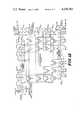
- FIG. 1illustrates the penetration depth of photons into silicon with the cross section of two diodes according to the present invention
- FIG. 2illustrates the estimated component quantum efficiencies for the two photodiode elements shown in FIG. 1;
- FIG. 3illustrates the total response plotted from the estimated components of two photodiodes
- FIG. 4illustrates schematically two epitaxially formed diode elements according to present invention
- FIG. 5illustrates two diodes in cross section and a epitaxial element with a deep collection diffusion
- FIG. 6illustrates a specific masking layout to implement a dual spectrum diode pair
- FIG. 7illustrates a dual spectrum array of two photodiode devices with a single V-groove making contact with the buried diffusion region
- FIG. 8illustrates a dual spectrum epitaxial photodiode element with a double V-groove
- FIG. 9illustrates a dual spectrum photodiode element schematic with separate video output lines
- FIG. 10is a photo mask composite of the dual spectrum photodiode element schematic with separate video output lines
- FIG. 11is a dual spectrum epitaxial array shift register schematic diagram
- FIG. 12is a schematic of a dual spectrum array of 12 by 38 elements.
- the sharply increasing optical absorption coefficient of silicon for wavelengths in the visible and infrared rangeresult in visible wavelength photons being absorbed near the silicon surface and infrared wavelengths photons penetrate further into the bulk silicon before absorption occurs. Therefore, photodiodes placed at the surface tend to response to visible photons and photodiodes placed deeper into the silicon bulk respond more to the infrared penetrating photons.
- FIG. 1shows schematically in FIG. 1 in which the absorption wavelength for photons of varying wavelengths is shown.
- the absorption length of 500 nanometers (nm) illuminationis approximately one micron. Illumination at 750 nm is 65% absorbed at 6.5 micron depth.
- a cell structureresults with separate visible and infrared photo responsivity.
- Present day technologies of silicon epitaxial crystal growth coupled with diffusion, ion implantation, and etching controlmake a photo-array cell possible. Since well known semiconductor processing techniques are used to produce the multi-spectrum device, details of the actual semiconductor process for making the device will not be explained in detail.
- the basic photodevice used in photodiode arraysis a shallow P-N junction near the surface, ohmic contacts to the diffused area and substrate together with appropriate voltage biasing circuitry.
- Self-scanned arraysare fabricated with a boron, p-type diffusion into silicon n-type substrate of resistivity 4-to-7 ohm-cm.
- the diode static characteristicfollows the diode equation.
- a jis the diode active area.
- the parameter V Fis forward diode bias.
- ⁇ n and ⁇ pare electron and hole lifetimes.
- Other parametersare standard semiconductor physics notation.
- ⁇ ois incident light flux (photons/cm 2 ).
- ⁇is the optical absorption coefficient (cm -1 ).
- L n and L pare surface dominated effects while those with L p are bulk hole carrier generation.
- L n and L p termsare surface dominated effects while those with L p are bulk hole carrier generation.
- Equation 9When Equation 9 is expressed in terms of minority carrier lifetime ⁇ and carrier diffusivity D, using Equation 10. ##EQU4## we obtain ##EQU5##
- the dark current I o in Equation 1was measured to be less than 2 picoamps for most processed devices. The result is a dark current I o two orders of magnitude reduced from those photocurrents I.sub. ⁇ obtained at nominal illumination levels ⁇ nom .
- the theory for the dual-spectrum epitaxial array cellrequires consideration of photoabsorption at the different penetration depths and selective collection of the generated carriers by photodiodes D 1 and D 2 .
- the carrier generation above the surface diode D 1 and below the buried diode D 2each contribute entirely to these two respective diode photocurrents.
- Carrier generation in the epitaxial volume between the two photodiodescontributes partially to both diodes D 1 and D 2 .
- the optical absorption processhere is spontaneous without wavecoupling.
- the hole-electron pairs in the epitaxial region d 1 ⁇ x ⁇ d 2diffuse isotropically in a 4 ⁇ stearadian pattern from each statistical generation site.
- a more detailed analysis for the epitaxial cellwill include the photocurrent contributions due to recombination within the depletion regions and the buried p-type film.
- the calculation for photocurrents in the dual-spectrum, lateral cellrequires modification of the incident flux to include the filtering effect of the overlaying polysilicon.
- T F ( ⁇ )is the spectral transmission of the polysilicon film and ⁇ o 1 is the filtered illumination entering the silicon surface.
- ⁇ o 1is the filtered illumination entering the silicon surface.
- the device illustrated in FIG. 1shows a surface diode D 1 formed by a p-type diffusion into a p-type epitaxial layer on an n-type substrate. Buried p-type region in the n-substrate forms the buried diode D 2 . A diffusion makes contact with the buried region.
- FIG. 2The quantum contributions from the semiconductor bulk and the two diode regions of FIG. 1 are shown in FIG. 2.
- the resulting quantum of efficiencyis shown in FIG. 3 for the surface diode D1 and buried diode D2.
- the filtering action of the siliconis evident in causing a shift in quantum efficiency for the photodiode D2 into the infrared region.
- FIG. 4is the schematic diagram of two "piggy-back" diodes with separate visible and infrared response.
- the column select in row A select lineare those which would normally be used for a semiconductor photodiode array.
- a row B select lineis added with transistors Q3 and Q4.
- a common video lineis used to provide output into the OCR system.
- Transistors Q1 and Q2are used to gate the video from diode D1 and transistors Q3 and Q4 are used to gate the video of D2 to the video line.
- FIG. 5is a cross section of a semiconductor device incorporating the features of the circuits shown in FIG. 4.
- Standard surface MOS transistorsare used at the Q1 to Q4 positions.
- a buried diodeis obtained by a diffusion or ion implant into the substrate and then covering it with an epitaxial film.
- Contact with the buried photodiodeis obtained by a deep diffusion similar to the diffusion-under-film collector contact diffusion common in bipolar IC processing and used for reducing the parameter R cs .
- the visible spectrumwill be detected by the photodiode D1
- the infrared spectrumwould be detected by the diode D2.
- the column select linesare P diffusions into the epitaxial layer.
- FIG. 6shows a specific masking layout to implement the dual spectrum cells of FIG. 4 and 5.
- a seventh maskis used to define the deep diffusion to the photodiode.
- the masking layoutcan be implemented on 4 mil centers with a slight reduction in the photodiode area to make space for the one added row address line.
- Each of the various regionsare identified by the legend shown in FIG. 6.
- FIG. 7is a cross sectional view of the semiconductor device in which a V-groove MOS transistor is used.
- An advantage of the V-groove technology in contacting the buried diffused regionis providing the MOS device while contacting the buried P diffusion number 1 which forms a part of diode D2.
- the buried layeris contacted by the V-groove which has been etched to the correct depth.
- the dual spectrum cell illustrated in FIG. 4can also be implemented with V-groove transistors at all four positions as illustrated in FIG. 8. Since the V-groove transistor requires less lateral area compared with the standard silicon-gate MOS transistor, more area within the cell is available for the active photodiodes.
- the buried photodiode D2is selected by the V-groove MOS transistor in the left half area of the cell.
- the one V-groove transistorrequires an extra mask for channel definition.
- the cellcan be designed with 4 mil by 4 mil array spacing or other desired spacings.
- the processing for the device in FIG. 8requires 7 photo mask levels plus protective passivation and is compatible with present day V-groove technology.
- infrared response enhancementis to cover a photodiode with a sufficiently thick film of polysilicon.
- the covering of polysilicon filmdoes not have the sharp absorption versus wavelength cutoff of single crystal silicon, but does permit an approximate visible filter.
- Another disadvantage of cell with covering polysilicon film foris that the total spectral response is reduced 50% compared with the buried diode design.
- a separate linemay be used for each diode or preferably a single video line is used.
- Output from each diodeis multiplexed into the single video line.
- the use of a single video output linereduces the shadow that would be caused by a second video port. Addressing of the cell for time multiplexing video into a single line output port is relatively simple. However, if a second video output port is required, it may be as illustrated in FIG. 9.
- FIG. 10A composite mask layout for a dual video port device is shown in FIG. 10.
- FIG. 11A single row address shift register for use with the dual video port array cell of FIG. 9 is illustrated in FIG. 11.
- the address circuit of FIG. 11uses 5 transistors per delay element.
- the complete dual array and all address and control elementsmay be formed in a semiconductor device using known integrated circuit design techniques and processes.
- FIG. 12To illustrate a complete photodiode array utilizing the dual spectrum diodes a schematic of a 12 by 38 array is shown in FIG. 12. This circuit shows a dual spectrum of two separate row address shift registers in a schematic layout with a single video port. The entire circuit may be implemented on a single semiconductor body.
- dual spectrum photodiodesmay be formed in a single semiconductor body for detecting and reading data having different wavelengths.
- Such devicesmay be extended to have 3 photodiodes, one each responsive to the red, green and blue spectra thereby using an array of such devices as an image pickup device with integral color separation. With present day technology these devices are feasible and an entire array with row and a column addressing circuits for multi-spectral output implemented within a single semiconductor body.
Landscapes
- Light Receiving Elements (AREA)
- Facsimile Heads (AREA)
- Solid State Image Pick-Up Elements (AREA)
Abstract
Description
I=I.sub.o [exp(qV.sub.F /kT)-1]-I.sub.λ (1)
G(x)=Φ.sub.o αexp(-αx) (3)
M(D)=G(x)exp[-|d-x|/L] (4)
M(d)=M.sub.P (d)+M.sub.n (d) (7)
______________________________________ Volume 1 0 < x < d.sub.1Volume 2 d.sub.1 < x < d.sub.2Volume 3 d.sub.2 < x < d.sub.3 ______________________________________
M.sub.1 =M.sub.1p +M.sub.1n (16)
M.sub.2 =M.sub.2na +M.sub.2nb (19)
Φ.sub.o.sup.1 =T.sub.F (λ)Φo (20)
Claims (6)
Priority Applications (7)
| Application Number | Priority Date | Filing Date | Title |
|---|---|---|---|
| US05/949,346US4238760A (en) | 1978-10-06 | 1978-10-06 | Multi-spectrum photodiode devices |
| CA000336322ACA1138081A (en) | 1978-10-06 | 1979-09-25 | Multi-spectrum photodiode devices |
| DE19792940343DE2940343A1 (en) | 1978-10-06 | 1979-10-04 | PHOTODIODE DEVICE |
| GB7934536AGB2034971A (en) | 1978-10-06 | 1979-10-04 | Multi-spectrum photosensitive devices |
| NL7907416ANL7907416A (en) | 1978-10-06 | 1979-10-05 | PHOTO DIODE. |
| FR7924822AFR2438344A1 (en) | 1978-10-06 | 1979-10-05 | MULTIPLE SPECTRUM PHOTOSENSITIVE DEVICE, IN PARTICULAR FOR OPTICAL CHARACTER READING |
| JP12849179AJPS5552277A (en) | 1978-10-06 | 1979-10-06 | Multiple spectrum photodiode device* photosensitive semiconductor device and method of manufacturing same |
Applications Claiming Priority (1)
| Application Number | Priority Date | Filing Date | Title |
|---|---|---|---|
| US05/949,346US4238760A (en) | 1978-10-06 | 1978-10-06 | Multi-spectrum photodiode devices |
Publications (1)
| Publication Number | Publication Date |
|---|---|
| US4238760Atrue US4238760A (en) | 1980-12-09 |
Family
ID=25488951
Family Applications (1)
| Application Number | Title | Priority Date | Filing Date |
|---|---|---|---|
| US05/949,346Expired - LifetimeUS4238760A (en) | 1978-10-06 | 1978-10-06 | Multi-spectrum photodiode devices |
Country Status (7)
| Country | Link |
|---|---|
| US (1) | US4238760A (en) |
| JP (1) | JPS5552277A (en) |
| CA (1) | CA1138081A (en) |
| DE (1) | DE2940343A1 (en) |
| FR (1) | FR2438344A1 (en) |
| GB (1) | GB2034971A (en) |
| NL (1) | NL7907416A (en) |
Cited By (72)
| Publication number | Priority date | Publication date | Assignee | Title |
|---|---|---|---|---|
| US4547792A (en)* | 1980-06-19 | 1985-10-15 | Rockwell International Corporation | Selective access array integrated circuit |
| US4651001A (en)* | 1983-12-19 | 1987-03-17 | Kabushiki Kaisha Toshiba | Visible/infrared imaging device with stacked cell structure |
| US4939369A (en)* | 1988-10-04 | 1990-07-03 | Loral Fairchild Corporation | Imaging and tracking sensor designed with a sandwich structure |
| GB2228824A (en)* | 1989-03-01 | 1990-09-05 | Gen Electric Co Plc | Radiation detectors |
| US5121377A (en)* | 1988-04-19 | 1992-06-09 | Bose Corporation | Error detection method and apparatus for reducing the number of errors generated when reading digital data stored on a recording medium such as film |
| US5466962A (en)* | 1993-04-19 | 1995-11-14 | Sharp Kabushiki Kaisha | Light-receiving semiconductor device with plural buried layers |
| EP0543361A3 (en)* | 1991-11-20 | 1997-09-03 | Canon Kk | Semiconductor device and method of manufacturing the same |
| US5942775A (en)* | 1997-04-30 | 1999-08-24 | Lucent Technologies Inc. | Photosensing device with improved spectral response and low thermal leakage |
| EP1078233A4 (en)* | 1998-04-24 | 2001-08-08 | Foveon Inc | COLOR SEPARATION IN AN ACTIVE PIXEL CELL MOSAIC USING A THREE-TUNNEL STRUCTURE |
| US6410899B1 (en) | 1998-06-17 | 2002-06-25 | Foveon, Inc. | Active pixel sensor with bootstrap amplification and reduced leakage during readout |
| US6433373B1 (en)* | 2000-04-28 | 2002-08-13 | Hynix Semiconductor Inc. | CMOS image sensor and a fabrication method for the same |
| US20020190254A1 (en)* | 2001-06-18 | 2002-12-19 | Turner Richard M. | Vertical color filter detector group and array |
| WO2002027804A3 (en)* | 2000-09-25 | 2003-02-20 | Foveon Inc | Vertical color filter detector group and array |
| US20030144779A1 (en)* | 2002-01-31 | 2003-07-31 | Denso Corporation | Automotive power distribution apparatus and auxiliary terminal for a user optional load |
| US6606120B1 (en) | 1998-04-24 | 2003-08-12 | Foveon, Inc. | Multiple storage node full color active pixel sensors |
| US6697114B1 (en)* | 1999-08-13 | 2004-02-24 | Foveon, Inc. | Triple slope pixel sensor and arry |
| US20040125222A1 (en)* | 2002-12-30 | 2004-07-01 | Bradski Gary R. | Stacked semiconductor radiation sensors having color component and infrared sensing capability |
| US6760070B1 (en) | 2000-02-29 | 2004-07-06 | Foveon, Inc. | High-sensitivity storage pixel sensor array having auto-exposure detection |
| US20040178466A1 (en)* | 2003-01-31 | 2004-09-16 | Foveon, Inc. | Vertical color filter sensor group and semiconductor integrated circuit fabrication method for fabricating same |
| US20040178467A1 (en)* | 2002-03-20 | 2004-09-16 | Foveon, Inc. | Vertical color filter sensor group array that emulates a pattern of single-layer sensors with efficient use of each sensor group's sensors |
| US20040178464A1 (en)* | 2003-01-31 | 2004-09-16 | Foveon, Inc. | Vertical color filter sensor group including semiconductor other than crystalline silicon and method for fabricating same |
| US20040185597A1 (en)* | 2001-06-18 | 2004-09-23 | Foveon, Inc. | Simplified wiring schemes for vertical color filter pixel sensors |
| US6809768B1 (en) | 2000-02-14 | 2004-10-26 | Foveon, Inc. | Double slope pixel sensor and array |
| US6841816B2 (en) | 2002-03-20 | 2005-01-11 | Foveon, Inc. | Vertical color filter sensor group with non-sensor filter and method for fabricating such a sensor group |
| US20050087829A1 (en)* | 2002-03-20 | 2005-04-28 | Merrill Richard B. | Vertical color filter sensor group with carrier-collection elements of different size and method for fabricating such a sensor group |
| US20050133704A1 (en)* | 2003-12-22 | 2005-06-23 | Hillis W. D. | Augmented photo-detector filter |
| US20050134489A1 (en)* | 2003-12-19 | 2005-06-23 | Hillis W. D. | Analog-to-digital converter circuitry having a cascade |
| US20050151057A1 (en)* | 2004-01-14 | 2005-07-14 | Hillis W. D. | Photo-detector filter having a cascaded low noise amplifier |
| US6930336B1 (en) | 2001-06-18 | 2005-08-16 | Foveon, Inc. | Vertical-color-filter detector group with trench isolation |
| US20050189475A1 (en)* | 2003-12-19 | 2005-09-01 | Hillis W. D. | Intensity detector circuitry |
| US20050205954A1 (en)* | 2002-12-18 | 2005-09-22 | King Clifford A | Image sensor comprising isolated germanium photodetectors integrated with a silicon substrate and silicon circuitry |
| US20050285038A1 (en)* | 2002-05-22 | 2005-12-29 | Beth Israel Deaconess Medical Center | Device for wavelength-selective imaging |
| US20060055800A1 (en)* | 2002-12-18 | 2006-03-16 | Noble Device Technologies Corp. | Adaptive solid state image sensor |
| US20060087646A1 (en)* | 2003-12-22 | 2006-04-27 | Searete Llc, A Limited Liability Corporation Of The State Of Delaware | Photo-detector filter |
| US20060114551A1 (en)* | 2003-11-10 | 2006-06-01 | Matsushita Electric Industrial Co., Ltd. | Imaging device and an imaging method |
| WO2006122425A1 (en)* | 2005-05-20 | 2006-11-23 | Tir Systems Ltd. | Multicolour chromaticity sensor |
| US7164444B1 (en) | 2002-05-17 | 2007-01-16 | Foveon, Inc. | Vertical color filter detector group with highlight detector |
| RU2311702C1 (en)* | 2006-03-01 | 2007-11-27 | Общество с ограниченной ответственностью ООО "Юник Ай Сиз" | Method for manufacturing group of transistors and photodetectors with vertical color filter |
| US20070292051A1 (en)* | 2006-06-16 | 2007-12-20 | Fujifilm Corporation | Information reader |
| KR100800310B1 (en)* | 2006-02-16 | 2008-02-01 | 마루엘에스아이 주식회사 | Optical sensing element capable of detecting visible light and infrared light and its manufacturing method |
| US7339216B1 (en) | 2003-01-31 | 2008-03-04 | Foveon, Inc. | Vertical color filter sensor group array with full-resolution top layer and lower-resolution lower layer |
| US20080116355A1 (en)* | 2003-12-19 | 2008-05-22 | Searete Llc, A Limited Liability Corporation Of The State Of Delaware | Photo-detector filter having a cascaded low noise amplifier |
| US20080135727A1 (en)* | 2003-12-19 | 2008-06-12 | Searete Llc, A Limited Liability Corporation Of The State Of Delaware | Photo-detector filter having a cascaded low noise amplifier |
| US20090021598A1 (en)* | 2006-12-06 | 2009-01-22 | Mclean John | Miniature integrated multispectral/multipolarization digital camera |
| WO2009046268A1 (en)* | 2007-10-04 | 2009-04-09 | Magna Electronics | Combined rgb and ir imaging sensor |
| US7602430B1 (en) | 2007-04-18 | 2009-10-13 | Foveon, Inc. | High-gain multicolor pixel sensor with reset noise cancellation |
| US20090303467A1 (en)* | 2006-07-18 | 2009-12-10 | Ian Ashdown | Method and apparatus for determining intensities and peak wavelengths of light |
| US20100019154A1 (en)* | 2008-07-28 | 2010-01-28 | Noble Peak Vision Corp. | Imaging apparatus and methods |
| WO2010044826A2 (en) | 2008-10-16 | 2010-04-22 | Eastman Kodak Company | Image sensor having multiple sensing layers |
| US20100102229A1 (en)* | 2008-10-28 | 2010-04-29 | Sony Ericsson Mobile Communications Ab | Combined sensor for portable communication devices |
| US20100102366A1 (en)* | 2008-10-24 | 2010-04-29 | Jong-Jan Lee | Integrated Infrared and Color CMOS Imager Sensor |
| US7745773B1 (en) | 2008-04-11 | 2010-06-29 | Foveon, Inc. | Multi-color CMOS pixel sensor with shared row wiring and dual output lines |
| US20100187406A1 (en)* | 2007-07-25 | 2010-07-29 | Nxp B.V. | Indoor/outdoor detection |
| US20100225628A1 (en)* | 2007-07-30 | 2010-09-09 | Nxp B.V. | Light sensor arrangement |
| US20100321225A1 (en)* | 2003-12-19 | 2010-12-23 | Searete Llc, A Limited Liability Corporation Of The State Of Delaware | Photo-detector filter having a cascaded low noise amplifier |
| US20110095188A1 (en)* | 2008-02-08 | 2011-04-28 | Omnivision Technologies, Inc. | Backside illuminated imaging sensor with improved infrared sensitivity |
| US20110169116A1 (en)* | 2010-01-13 | 2011-07-14 | Fei Company | Radiation Detector |
| US20110175188A1 (en)* | 2010-01-19 | 2011-07-21 | Peter Steven Bui | Wavelength Sensitive Sensor Photodiodes |
| US8084739B2 (en) | 2008-07-16 | 2011-12-27 | Infrared Newco., Inc. | Imaging apparatus and methods |
| WO2011162636A1 (en)* | 2010-06-25 | 2011-12-29 | Phyedosyeyenko Alyeksyej Olyegovich | Method for recording an optical signal, device for implementing same and method for scanning an object |
| US20120085890A1 (en)* | 2010-10-07 | 2012-04-12 | Semiconductor Energy Laboratory Co., Ltd. | Photodetector |
| US20130322729A1 (en)* | 2012-05-30 | 2013-12-05 | Xerox Corporation | Processing a video for vascular pattern detection and cardiac function analysis |
| US8816464B2 (en) | 2008-08-27 | 2014-08-26 | Osi Optoelectronics, Inc. | Photodiode and photodiode array with improved performance characteristics |
| US8907440B2 (en) | 2003-05-05 | 2014-12-09 | Osi Optoelectronics, Inc. | High speed backside illuminated, front side contact photodiode array |
| US8912615B2 (en) | 2013-01-24 | 2014-12-16 | Osi Optoelectronics, Inc. | Shallow junction photodiode for detecting short wavelength light |
| US9035412B2 (en) | 2007-05-07 | 2015-05-19 | Osi Optoelectronics, Inc. | Thin active layer fishbone photodiode with a shallow N+ layer and method of manufacturing the same |
| US9147777B2 (en) | 2009-05-12 | 2015-09-29 | Osi Optoelectronics, Inc. | Tetra-lateral position sensing detector |
| US9231015B2 (en) | 2012-09-24 | 2016-01-05 | Omnivision Technologies, Inc. | Backside-illuminated photosensor array with white, yellow and red-sensitive elements |
| US9455291B2 (en) | 2015-01-20 | 2016-09-27 | Omnivision Technologies, Inc. | Blue enhanced image sensor |
| US9565405B2 (en) | 2015-02-03 | 2017-02-07 | Omnivision Technologies, Inc. | Image sensor with enhanced quantum efficiency |
| US9751465B2 (en) | 2012-04-16 | 2017-09-05 | Magna Electronics Inc. | Vehicle vision system with reduced image color data processing by use of dithering |
| US20220359481A1 (en)* | 2010-04-21 | 2022-11-10 | Sionyx, Llc | Photosensitive imaging devices and associated methods |
Families Citing this family (12)
| Publication number | Priority date | Publication date | Assignee | Title |
|---|---|---|---|---|
| FR2514205A1 (en)* | 1981-10-05 | 1983-04-08 | Merlin Gerin | TERMINAL FOR CONNECTING CONDUCTIVE CABLES TO AN ELECTRICAL APPARATUS |
| US4533940A (en)* | 1983-06-13 | 1985-08-06 | Chappell Barbara A | High spatial resolution energy discriminator |
| JPS60164354A (en)* | 1984-02-06 | 1985-08-27 | Victor Co Of Japan Ltd | solid-state imaging device |
| DE4243421A1 (en)* | 1992-12-16 | 1993-07-29 | Medium Sensor Gmbh | Opto-electronic component for measuring limited region of ultraviolet radiation - contains fluorescent medium stimulated by ultraviolet, optical and filtering arrangement ensuring narrow spectral stimulation region |
| US6946715B2 (en)* | 2003-02-19 | 2005-09-20 | Micron Technology, Inc. | CMOS image sensor and method of fabrication |
| KR100760142B1 (en)* | 2005-07-27 | 2007-09-18 | 매그나칩 반도체 유한회사 | Stacked Pixels for High Resolution CMOS Image Sensors |
| JP4839990B2 (en)* | 2006-07-06 | 2011-12-21 | 株式会社ニコン | Solid-state imaging device and imaging apparatus using the same |
| JP5045012B2 (en)* | 2006-07-20 | 2012-10-10 | 株式会社ニコン | Solid-state imaging device and imaging apparatus using the same |
| JP5670456B2 (en)* | 2009-08-25 | 2015-02-18 | アイピーリンク・リミテッド | Reduce noise in color images |
| FR2969390B1 (en)* | 2010-12-15 | 2014-09-26 | St Microelectronics Rousset | IMAGING DEVICE WITH INFRARED RADIATION FILTRATION. |
| US20160255323A1 (en) | 2015-02-26 | 2016-09-01 | Dual Aperture International Co. Ltd. | Multi-Aperture Depth Map Using Blur Kernels and Down-Sampling |
| JP6755679B2 (en)* | 2016-03-04 | 2020-09-16 | キヤノン株式会社 | Imaging device |
Citations (7)
| Publication number | Priority date | Publication date | Assignee | Title |
|---|---|---|---|---|
| US3478214A (en)* | 1966-02-16 | 1969-11-11 | North American Rockwell | Photodetector responsive to light intensity in different spectral bands |
| US3812518A (en)* | 1973-01-02 | 1974-05-21 | Gen Electric | Photodiode with patterned structure |
| US3964083A (en)* | 1973-06-14 | 1976-06-15 | U.S. Philips Corporation | Punchthrough resetting jfet image sensor |
| US4011016A (en)* | 1974-04-30 | 1977-03-08 | Martin Marietta Corporation | Semiconductor radiation wavelength detector |
| US4048649A (en)* | 1976-02-06 | 1977-09-13 | Transitron Electronic Corporation | Superintegrated v-groove isolated bipolar and vmos transistors |
| US4084175A (en)* | 1976-09-30 | 1978-04-11 | Research Corporation | Double implanted planar mos device with v-groove and process of manufacture thereof |
| US4109270A (en)* | 1976-05-04 | 1978-08-22 | Siemens Aktiengesellschaft | Semiconductor store |
Family Cites Families (2)
| Publication number | Priority date | Publication date | Assignee | Title |
|---|---|---|---|---|
| US3413603A (en)* | 1964-04-22 | 1968-11-26 | Kimura Kenjiro | Semiconductor character sensing device |
| LU71811A1 (en)* | 1975-02-07 | 1975-06-24 |
- 1978
- 1978-10-06USUS05/949,346patent/US4238760A/ennot_activeExpired - Lifetime
- 1979
- 1979-09-25CACA000336322Apatent/CA1138081A/ennot_activeExpired
- 1979-10-04DEDE19792940343patent/DE2940343A1/ennot_activeCeased
- 1979-10-04GBGB7934536Apatent/GB2034971A/ennot_activeWithdrawn
- 1979-10-05NLNL7907416Apatent/NL7907416A/ennot_activeApplication Discontinuation
- 1979-10-05FRFR7924822Apatent/FR2438344A1/ennot_activeWithdrawn
- 1979-10-06JPJP12849179Apatent/JPS5552277A/enactivePending
Patent Citations (7)
| Publication number | Priority date | Publication date | Assignee | Title |
|---|---|---|---|---|
| US3478214A (en)* | 1966-02-16 | 1969-11-11 | North American Rockwell | Photodetector responsive to light intensity in different spectral bands |
| US3812518A (en)* | 1973-01-02 | 1974-05-21 | Gen Electric | Photodiode with patterned structure |
| US3964083A (en)* | 1973-06-14 | 1976-06-15 | U.S. Philips Corporation | Punchthrough resetting jfet image sensor |
| US4011016A (en)* | 1974-04-30 | 1977-03-08 | Martin Marietta Corporation | Semiconductor radiation wavelength detector |
| US4048649A (en)* | 1976-02-06 | 1977-09-13 | Transitron Electronic Corporation | Superintegrated v-groove isolated bipolar and vmos transistors |
| US4109270A (en)* | 1976-05-04 | 1978-08-22 | Siemens Aktiengesellschaft | Semiconductor store |
| US4084175A (en)* | 1976-09-30 | 1978-04-11 | Research Corporation | Double implanted planar mos device with v-groove and process of manufacture thereof |
Cited By (150)
| Publication number | Priority date | Publication date | Assignee | Title |
|---|---|---|---|---|
| US4547792A (en)* | 1980-06-19 | 1985-10-15 | Rockwell International Corporation | Selective access array integrated circuit |
| US4651001A (en)* | 1983-12-19 | 1987-03-17 | Kabushiki Kaisha Toshiba | Visible/infrared imaging device with stacked cell structure |
| US5121377A (en)* | 1988-04-19 | 1992-06-09 | Bose Corporation | Error detection method and apparatus for reducing the number of errors generated when reading digital data stored on a recording medium such as film |
| US4939369A (en)* | 1988-10-04 | 1990-07-03 | Loral Fairchild Corporation | Imaging and tracking sensor designed with a sandwich structure |
| GB2228824A (en)* | 1989-03-01 | 1990-09-05 | Gen Electric Co Plc | Radiation detectors |
| EP0543361A3 (en)* | 1991-11-20 | 1997-09-03 | Canon Kk | Semiconductor device and method of manufacturing the same |
| US5952694A (en)* | 1991-11-20 | 1999-09-14 | Canon Kabushiki Kaisha | Semiconductor device made using processing from both sides of a workpiece |
| US5466962A (en)* | 1993-04-19 | 1995-11-14 | Sharp Kabushiki Kaisha | Light-receiving semiconductor device with plural buried layers |
| US5942775A (en)* | 1997-04-30 | 1999-08-24 | Lucent Technologies Inc. | Photosensing device with improved spectral response and low thermal leakage |
| US6606120B1 (en) | 1998-04-24 | 2003-08-12 | Foveon, Inc. | Multiple storage node full color active pixel sensors |
| CN100416241C (en)* | 1998-04-24 | 2008-09-03 | 福维昂公司 | Color separation in active pixel cell imaging matrices using triple well structures |
| EP1078233A4 (en)* | 1998-04-24 | 2001-08-08 | Foveon Inc | COLOR SEPARATION IN AN ACTIVE PIXEL CELL MOSAIC USING A THREE-TUNNEL STRUCTURE |
| US20030169359A1 (en)* | 1998-04-24 | 2003-09-11 | Foven, Inc. A California Corporation | Multiple storage node full color active pixel sensors |
| US6410899B1 (en) | 1998-06-17 | 2002-06-25 | Foveon, Inc. | Active pixel sensor with bootstrap amplification and reduced leakage during readout |
| US6697114B1 (en)* | 1999-08-13 | 2004-02-24 | Foveon, Inc. | Triple slope pixel sensor and arry |
| US6809768B1 (en) | 2000-02-14 | 2004-10-26 | Foveon, Inc. | Double slope pixel sensor and array |
| US6882367B1 (en) | 2000-02-29 | 2005-04-19 | Foveon, Inc. | High-sensitivity storage pixel sensor having auto-exposure detection |
| US6760070B1 (en) | 2000-02-29 | 2004-07-06 | Foveon, Inc. | High-sensitivity storage pixel sensor array having auto-exposure detection |
| US6433373B1 (en)* | 2000-04-28 | 2002-08-13 | Hynix Semiconductor Inc. | CMOS image sensor and a fabrication method for the same |
| US6610557B2 (en) | 2000-04-28 | 2003-08-26 | Hynix Semiconductor Inc. | CMOS image sensor and a fabrication method for the same |
| US7132724B1 (en) | 2000-09-25 | 2006-11-07 | Foveon, Inc. | Complete-charge-transfer vertical color filter detector |
| US6727521B2 (en) | 2000-09-25 | 2004-04-27 | Foveon, Inc. | Vertical color filter detector group and array |
| US6632701B2 (en)* | 2000-09-25 | 2003-10-14 | Foveon, Inc. | Vertical color filter detector group and array |
| WO2002027804A3 (en)* | 2000-09-25 | 2003-02-20 | Foveon Inc | Vertical color filter detector group and array |
| US20020190254A1 (en)* | 2001-06-18 | 2002-12-19 | Turner Richard M. | Vertical color filter detector group and array |
| US6864557B2 (en) | 2001-06-18 | 2005-03-08 | Foveon, Inc. | Vertical color filter detector group and array |
| US6930336B1 (en) | 2001-06-18 | 2005-08-16 | Foveon, Inc. | Vertical-color-filter detector group with trench isolation |
| US20040185597A1 (en)* | 2001-06-18 | 2004-09-23 | Foveon, Inc. | Simplified wiring schemes for vertical color filter pixel sensors |
| US6960757B2 (en) | 2001-06-18 | 2005-11-01 | Foveon, Inc. | Simplified wiring schemes for vertical color filter pixel sensors |
| US20030144779A1 (en)* | 2002-01-31 | 2003-07-31 | Denso Corporation | Automotive power distribution apparatus and auxiliary terminal for a user optional load |
| US6998660B2 (en) | 2002-03-20 | 2006-02-14 | Foveon, Inc. | Vertical color filter sensor group array that emulates a pattern of single-layer sensors with efficient use of each sensor group's sensors |
| US6841816B2 (en) | 2002-03-20 | 2005-01-11 | Foveon, Inc. | Vertical color filter sensor group with non-sensor filter and method for fabricating such a sensor group |
| US20050087829A1 (en)* | 2002-03-20 | 2005-04-28 | Merrill Richard B. | Vertical color filter sensor group with carrier-collection elements of different size and method for fabricating such a sensor group |
| US7166880B2 (en) | 2002-03-20 | 2007-01-23 | Foveon, Inc. | Vertical color filter sensor group with carrier-collection elements of different size and method for fabricating such a sensor group |
| US20040178467A1 (en)* | 2002-03-20 | 2004-09-16 | Foveon, Inc. | Vertical color filter sensor group array that emulates a pattern of single-layer sensors with efficient use of each sensor group's sensors |
| US7164444B1 (en) | 2002-05-17 | 2007-01-16 | Foveon, Inc. | Vertical color filter detector group with highlight detector |
| US20050285038A1 (en)* | 2002-05-22 | 2005-12-29 | Beth Israel Deaconess Medical Center | Device for wavelength-selective imaging |
| US20100305455A1 (en)* | 2002-05-22 | 2010-12-02 | Frangioni John V | Device for wavelength-selective imaging |
| US7794394B2 (en) | 2002-05-22 | 2010-09-14 | Beth Israel Deaconess Medical Center | Device for wavelength-selective imaging |
| US20090072284A1 (en)* | 2002-12-18 | 2009-03-19 | Noble Peak Vision Corp. | Image sensor comprising isolated germanium photodetectors integrated with a silicon substrate and silicon circuitry |
| US20050205954A1 (en)* | 2002-12-18 | 2005-09-22 | King Clifford A | Image sensor comprising isolated germanium photodetectors integrated with a silicon substrate and silicon circuitry |
| US7453129B2 (en) | 2002-12-18 | 2008-11-18 | Noble Peak Vision Corp. | Image sensor comprising isolated germanium photodetectors integrated with a silicon substrate and silicon circuitry |
| US7973377B2 (en) | 2002-12-18 | 2011-07-05 | Infrared Newco, Inc. | Image sensor comprising isolated germanium photodetectors integrated with a silicon substrate and silicon circuitry |
| US20060055800A1 (en)* | 2002-12-18 | 2006-03-16 | Noble Device Technologies Corp. | Adaptive solid state image sensor |
| US9142585B2 (en) | 2002-12-18 | 2015-09-22 | Infrared Newco, Inc. | Image sensor comprising isolated germanium photodetectors integrated with a silicon substrate and silicon circuitry |
| US8664739B2 (en) | 2002-12-18 | 2014-03-04 | Infrared Newco, Inc. | Image sensor comprising isolated germanium photodetectors integrated with a silicon substrate and silicon circuitry |
| US20040125222A1 (en)* | 2002-12-30 | 2004-07-01 | Bradski Gary R. | Stacked semiconductor radiation sensors having color component and infrared sensing capability |
| WO2004061966A1 (en)* | 2002-12-30 | 2004-07-22 | Intel Corporation | Stacked semiconductor radiation sensors having color component and infrared sensing capability |
| US7154157B2 (en) | 2002-12-30 | 2006-12-26 | Intel Corporation | Stacked semiconductor radiation sensors having color component and infrared sensing capability |
| US6914314B2 (en) | 2003-01-31 | 2005-07-05 | Foveon, Inc. | Vertical color filter sensor group including semiconductor other than crystalline silicon and method for fabricating same |
| US7339216B1 (en) | 2003-01-31 | 2008-03-04 | Foveon, Inc. | Vertical color filter sensor group array with full-resolution top layer and lower-resolution lower layer |
| US6894265B2 (en) | 2003-01-31 | 2005-05-17 | Foveon, Inc. | Vertical color filter sensor group and semiconductor integrated circuit fabrication method for fabricating same |
| US20040178464A1 (en)* | 2003-01-31 | 2004-09-16 | Foveon, Inc. | Vertical color filter sensor group including semiconductor other than crystalline silicon and method for fabricating same |
| US20040178466A1 (en)* | 2003-01-31 | 2004-09-16 | Foveon, Inc. | Vertical color filter sensor group and semiconductor integrated circuit fabrication method for fabricating same |
| US8907440B2 (en) | 2003-05-05 | 2014-12-09 | Osi Optoelectronics, Inc. | High speed backside illuminated, front side contact photodiode array |
| EP1630871A4 (en)* | 2003-11-10 | 2007-03-14 | Matsushita Electric Industrial Co Ltd | IMAGING DEVICE AND IMAGING METHOD |
| US7247851B2 (en)* | 2003-11-10 | 2007-07-24 | Matsushita Electric Industrial Co., Ltd. | Imaging device and an imaging method |
| US20060114551A1 (en)* | 2003-11-10 | 2006-06-01 | Matsushita Electric Industrial Co., Ltd. | Imaging device and an imaging method |
| CN100416843C (en)* | 2003-11-10 | 2008-09-03 | 松下电器产业株式会社 | Imaging device and imaging method |
| US8212196B2 (en) | 2003-12-19 | 2012-07-03 | The Invention Science Fund I, Llc | Photo-detector filter having a cascaded low noise amplifier |
| US7511254B2 (en) | 2003-12-19 | 2009-03-31 | Searete, Llc | Photo-detector filter having a cascaded low noise amplifier |
| US20100321225A1 (en)* | 2003-12-19 | 2010-12-23 | Searete Llc, A Limited Liability Corporation Of The State Of Delaware | Photo-detector filter having a cascaded low noise amplifier |
| US7045760B2 (en) | 2003-12-19 | 2006-05-16 | Searete Llc | Intensity detector circuitry |
| US7999214B2 (en) | 2003-12-19 | 2011-08-16 | The Invention Science Fund I, Llc | Photo-detector filter having a cascaded low noise amplifier |
| US7304289B2 (en) | 2003-12-19 | 2007-12-04 | Searete Llc | Intensity detector circuitry having plural gain elements in a cascade with plural threshold values |
| US7649164B2 (en) | 2003-12-19 | 2010-01-19 | Searete, Llc | Augmented photo-detector filter |
| US20060108512A1 (en)* | 2003-12-19 | 2006-05-25 | Hillis W D | Intensity detector circuitry |
| US20090302201A1 (en)* | 2003-12-19 | 2009-12-10 | Hillis W Daniel | Photo-detector filter having a cascaded low noise amplifier |
| US20080116355A1 (en)* | 2003-12-19 | 2008-05-22 | Searete Llc, A Limited Liability Corporation Of The State Of Delaware | Photo-detector filter having a cascaded low noise amplifier |
| US20080135727A1 (en)* | 2003-12-19 | 2008-06-12 | Searete Llc, A Limited Liability Corporation Of The State Of Delaware | Photo-detector filter having a cascaded low noise amplifier |
| US20060151681A1 (en)* | 2003-12-19 | 2006-07-13 | Searete Llc | Augmented photo-detector filter |
| US7515082B2 (en) | 2003-12-19 | 2009-04-07 | Searete, Llc | Photo-detector filter having a cascaded low noise amplifier |
| US20050134489A1 (en)* | 2003-12-19 | 2005-06-23 | Hillis W. D. | Analog-to-digital converter circuitry having a cascade |
| US20050189475A1 (en)* | 2003-12-19 | 2005-09-01 | Hillis W. D. | Intensity detector circuitry |
| US7053809B2 (en) | 2003-12-19 | 2006-05-30 | Searete Llc | Analog-to-digital converter circuitry having a cascade |
| US7929126B2 (en) | 2003-12-22 | 2011-04-19 | The Invention Science Fund I, Llc | Photo-detector filter |
| US7098439B2 (en)* | 2003-12-22 | 2006-08-29 | Searete Llc | Augmented photo-detector filter |
| US7542133B2 (en) | 2003-12-22 | 2009-06-02 | Searete, Llc | Photo-detector filter |
| US20100238432A1 (en)* | 2003-12-22 | 2010-09-23 | Hillis W Daniel | Photo-detector filter |
| US20050133704A1 (en)* | 2003-12-22 | 2005-06-23 | Hillis W. D. | Augmented photo-detector filter |
| WO2005065130A3 (en)* | 2003-12-22 | 2005-11-17 | Searete Llc | Augmented photo-detector filter |
| US20060087646A1 (en)* | 2003-12-22 | 2006-04-27 | Searete Llc, A Limited Liability Corporation Of The State Of Delaware | Photo-detector filter |
| US7053998B2 (en) | 2003-12-22 | 2006-05-30 | Searete Llc | Photo-detector filter |
| US7250595B2 (en) | 2004-01-14 | 2007-07-31 | Searete, Llc | Photo-detector filter having a cascaded low noise amplifier |
| US20050151057A1 (en)* | 2004-01-14 | 2005-07-14 | Hillis W. D. | Photo-detector filter having a cascaded low noise amplifier |
| US7388665B2 (en) | 2005-05-20 | 2008-06-17 | Tir Technology Lp | Multicolour chromaticity sensor |
| WO2006122425A1 (en)* | 2005-05-20 | 2006-11-23 | Tir Systems Ltd. | Multicolour chromaticity sensor |
| US20070051881A1 (en)* | 2005-05-20 | 2007-03-08 | Tir Systems Ltd. | Multicolour chromaticity sensor |
| KR100800310B1 (en)* | 2006-02-16 | 2008-02-01 | 마루엘에스아이 주식회사 | Optical sensing element capable of detecting visible light and infrared light and its manufacturing method |
| RU2311702C1 (en)* | 2006-03-01 | 2007-11-27 | Общество с ограниченной ответственностью ООО "Юник Ай Сиз" | Method for manufacturing group of transistors and photodetectors with vertical color filter |
| US20070292051A1 (en)* | 2006-06-16 | 2007-12-20 | Fujifilm Corporation | Information reader |
| US7629997B2 (en)* | 2006-06-16 | 2009-12-08 | Fujifilm Corporation | Information reader |
| US7894050B2 (en) | 2006-07-18 | 2011-02-22 | Koninklijke Philips Electronics N.V. | Method and apparatus for determining intensities and peak wavelengths of light |
| US20090303467A1 (en)* | 2006-07-18 | 2009-12-10 | Ian Ashdown | Method and apparatus for determining intensities and peak wavelengths of light |
| US20090021598A1 (en)* | 2006-12-06 | 2009-01-22 | Mclean John | Miniature integrated multispectral/multipolarization digital camera |
| US7602430B1 (en) | 2007-04-18 | 2009-10-13 | Foveon, Inc. | High-gain multicolor pixel sensor with reset noise cancellation |
| US9035412B2 (en) | 2007-05-07 | 2015-05-19 | Osi Optoelectronics, Inc. | Thin active layer fishbone photodiode with a shallow N+ layer and method of manufacturing the same |
| US8592744B2 (en)* | 2007-07-25 | 2013-11-26 | Nxp B.V. | Indoor/outdoor detection |
| US20100187406A1 (en)* | 2007-07-25 | 2010-07-29 | Nxp B.V. | Indoor/outdoor detection |
| US20100225628A1 (en)* | 2007-07-30 | 2010-09-09 | Nxp B.V. | Light sensor arrangement |
| US9019251B2 (en) | 2007-07-30 | 2015-04-28 | Nxp, B.V. | Light sensor arrangement |
| WO2009046268A1 (en)* | 2007-10-04 | 2009-04-09 | Magna Electronics | Combined rgb and ir imaging sensor |
| US10616507B2 (en) | 2007-10-04 | 2020-04-07 | Magna Electronics Inc. | Imaging system for vehicle |
| US11165975B2 (en) | 2007-10-04 | 2021-11-02 | Magna Electronics Inc. | Imaging system for vehicle |
| US8908040B2 (en) | 2007-10-04 | 2014-12-09 | Magna Electronics Inc. | Imaging system for vehicle |
| US8446470B2 (en) | 2007-10-04 | 2013-05-21 | Magna Electronics, Inc. | Combined RGB and IR imaging sensor |
| US20100289885A1 (en)* | 2007-10-04 | 2010-11-18 | Yuesheng Lu | Combined RGB and IR Imaging Sensor |
| US10003755B2 (en) | 2007-10-04 | 2018-06-19 | Magna Electronics Inc. | Imaging system for vehicle |
| US20110095188A1 (en)* | 2008-02-08 | 2011-04-28 | Omnivision Technologies, Inc. | Backside illuminated imaging sensor with improved infrared sensitivity |
| TWI407555B (en)* | 2008-02-08 | 2013-09-01 | Omnivision Tech Inc | Back side light receiving image sensor and control method thereof |
| US8329497B2 (en)* | 2008-02-08 | 2012-12-11 | Omnivision Technologies, Inc. | Backside illuminated imaging sensor with improved infrared sensitivity |
| US7745773B1 (en) | 2008-04-11 | 2010-06-29 | Foveon, Inc. | Multi-color CMOS pixel sensor with shared row wiring and dual output lines |
| US8084739B2 (en) | 2008-07-16 | 2011-12-27 | Infrared Newco., Inc. | Imaging apparatus and methods |
| US8294100B2 (en) | 2008-07-16 | 2012-10-23 | Infrared Newco, Inc. | Imaging apparatus and methods |
| US8686365B2 (en) | 2008-07-28 | 2014-04-01 | Infrared Newco, Inc. | Imaging apparatus and methods |
| US20100019154A1 (en)* | 2008-07-28 | 2010-01-28 | Noble Peak Vision Corp. | Imaging apparatus and methods |
| US8816464B2 (en) | 2008-08-27 | 2014-08-26 | Osi Optoelectronics, Inc. | Photodiode and photodiode array with improved performance characteristics |
| CN102177585B (en)* | 2008-10-16 | 2014-01-15 | 全视科技有限公司 | Image sensor with multiple sensing layers and method of operation and fabrication thereof |
| WO2010044826A2 (en) | 2008-10-16 | 2010-04-22 | Eastman Kodak Company | Image sensor having multiple sensing layers |
| WO2010044826A3 (en)* | 2008-10-16 | 2010-06-10 | Eastman Kodak Company | Image sensor having multiple sensing layers and its method of operation and fabrication |
| US8054355B2 (en) | 2008-10-16 | 2011-11-08 | Omnivision Technologies, Inc. | Image sensor having multiple sensing layers |
| US20100097514A1 (en)* | 2008-10-16 | 2010-04-22 | Mccarten John P | Image sensor having multiple sensing layers |
| US20100102366A1 (en)* | 2008-10-24 | 2010-04-29 | Jong-Jan Lee | Integrated Infrared and Color CMOS Imager Sensor |
| US7915652B2 (en) | 2008-10-24 | 2011-03-29 | Sharp Laboratories Of America, Inc. | Integrated infrared and color CMOS imager sensor |
| WO2010049183A1 (en)* | 2008-10-28 | 2010-05-06 | Sony Ericsson Mobile Communications Ab | Combined sensor for portable communication devices |
| US20100102229A1 (en)* | 2008-10-28 | 2010-04-29 | Sony Ericsson Mobile Communications Ab | Combined sensor for portable communication devices |
| US9577121B2 (en) | 2009-05-12 | 2017-02-21 | Osi Optoelectronics, Inc. | Tetra-lateral position sensing detector |
| US9147777B2 (en) | 2009-05-12 | 2015-09-29 | Osi Optoelectronics, Inc. | Tetra-lateral position sensing detector |
| EP2346095A2 (en) | 2010-01-13 | 2011-07-20 | Fei Company | Method of manufacturing a radiation detector |
| US20110169116A1 (en)* | 2010-01-13 | 2011-07-14 | Fei Company | Radiation Detector |
| US8450820B2 (en) | 2010-01-13 | 2013-05-28 | Lis Karen Nanver | Radiation detector |
| EP2346094A1 (en) | 2010-01-13 | 2011-07-20 | FEI Company | Method of manufacturing a radiation detector |
| US20140319642A1 (en)* | 2010-01-19 | 2014-10-30 | Osi Optoelectronics | Wavelength Sensitive Sensor Photodiodes |
| US8686529B2 (en)* | 2010-01-19 | 2014-04-01 | Osi Optoelectronics, Inc. | Wavelength sensitive sensor photodiodes |
| US9214588B2 (en)* | 2010-01-19 | 2015-12-15 | Osi Optoelectronics, Inc. | Wavelength sensitive sensor photodiodes |
| US20110175188A1 (en)* | 2010-01-19 | 2011-07-21 | Peter Steven Bui | Wavelength Sensitive Sensor Photodiodes |
| US11728322B2 (en)* | 2010-04-21 | 2023-08-15 | Sionyx, Llc | Photosensitive imaging devices and associated methods |
| US20220359481A1 (en)* | 2010-04-21 | 2022-11-10 | Sionyx, Llc | Photosensitive imaging devices and associated methods |
| WO2011162636A1 (en)* | 2010-06-25 | 2011-12-29 | Phyedosyeyenko Alyeksyej Olyegovich | Method for recording an optical signal, device for implementing same and method for scanning an object |
| US8987651B2 (en)* | 2010-10-07 | 2015-03-24 | Semiconductor Energy Laboratory Co., Ltd. | Photodetector including photodiodes overlapped with each other |
| US20120085890A1 (en)* | 2010-10-07 | 2012-04-12 | Semiconductor Energy Laboratory Co., Ltd. | Photodetector |
| US10434944B2 (en) | 2012-04-16 | 2019-10-08 | Magna Electronics Inc. | Vehicle vision system with reduced image color data processing by use of dithering |
| US9751465B2 (en) | 2012-04-16 | 2017-09-05 | Magna Electronics Inc. | Vehicle vision system with reduced image color data processing by use of dithering |
| US20130322729A1 (en)* | 2012-05-30 | 2013-12-05 | Xerox Corporation | Processing a video for vascular pattern detection and cardiac function analysis |
| US8897522B2 (en)* | 2012-05-30 | 2014-11-25 | Xerox Corporation | Processing a video for vascular pattern detection and cardiac function analysis |
| US9231015B2 (en) | 2012-09-24 | 2016-01-05 | Omnivision Technologies, Inc. | Backside-illuminated photosensor array with white, yellow and red-sensitive elements |
| US9691934B2 (en) | 2013-01-24 | 2017-06-27 | Osi Optoelectronics, Inc. | Shallow junction photodiode for detecting short wavelength light |
| US8912615B2 (en) | 2013-01-24 | 2014-12-16 | Osi Optoelectronics, Inc. | Shallow junction photodiode for detecting short wavelength light |
| US9455291B2 (en) | 2015-01-20 | 2016-09-27 | Omnivision Technologies, Inc. | Blue enhanced image sensor |
| US9565405B2 (en) | 2015-02-03 | 2017-02-07 | Omnivision Technologies, Inc. | Image sensor with enhanced quantum efficiency |
Also Published As
| Publication number | Publication date |
|---|---|
| NL7907416A (en) | 1980-04-09 |
| JPS5552277A (en) | 1980-04-16 |
| FR2438344A1 (en) | 1980-04-30 |
| DE2940343A1 (en) | 1980-04-10 |
| GB2034971A (en) | 1980-06-11 |
| CA1138081A (en) | 1982-12-21 |
Similar Documents
| Publication | Publication Date | Title |
|---|---|---|
| US4238760A (en) | Multi-spectrum photodiode devices | |
| US7132724B1 (en) | Complete-charge-transfer vertical color filter detector | |
| US6169318B1 (en) | CMOS imager with improved sensitivity | |
| US5965875A (en) | Color separation in an active pixel cell imaging array using a triple-well structure | |
| EP1004140B1 (en) | A well to substrate photodiode for use in a cmos sensor on a salicide process | |
| US4613895A (en) | Color responsive imaging device employing wavelength dependent semiconductor optical absorption | |
| US5162887A (en) | Buried junction photodiode | |
| US6465860B2 (en) | Multi-wavelength semiconductor image sensor and method of manufacturing the same | |
| US6489643B1 (en) | Photodiode having a plurality of PN junctions and image sensor having the same | |
| US6034407A (en) | Multi-spectral planar photodiode infrared radiation detector pixels | |
| US3551761A (en) | Integrated photodiode array | |
| US7427734B2 (en) | Multiple photosensor pixel | |
| US8946617B2 (en) | Photodiode having a p-n junction with varying expansion of the space charge zone due to application of a variable voltage | |
| CN101176208A (en) | Colored pixels with anti-blur isolation and method of formation | |
| US20070131992A1 (en) | Multiple photosensor pixel image sensor | |
| EP0166787B1 (en) | Colour image sensor | |
| US7671392B2 (en) | Photoreceiver cell with color separation | |
| US4920395A (en) | High sensitivity photodiode | |
| US5329149A (en) | Image sensor with non-light-transmissive layer having photosensing windows | |
| US4646120A (en) | Photodiode array | |
| US4673985A (en) | Semiconductor image sensor | |
| US5982011A (en) | Photodiode structure augmented with active area photosensitive regions | |
| US5177580A (en) | Implant guarded mesa having improved detector uniformity | |
| US4686761A (en) | Method of fabrication of low crosstalk photodiode array | |
| RU2297074C2 (en) | Photo-receiving cell with color division |
Legal Events
| Date | Code | Title | Description |
|---|---|---|---|
| AS | Assignment | Owner name:CHEMICAL BANK, A NY BANKING CORP. Free format text:SECURITY INTEREST;ASSIGNORS:RECOGNITION EQUIPMENT INCORPORATED;PLEXUS SOFTWARE, INC.;REEL/FRAME:005323/0509 Effective date:19891119 | |
| AS | Assignment | Owner name:RECOGNITION EQUIPMENT INCORPORATED ("REI") 2701 EA Free format text:RELEASED BY SECURED PARTY;ASSIGNOR:CHEMICAL BANK, A NY. BANKING CORP.;REEL/FRAME:005439/0823 Effective date:19900731 | |
| AS | Assignment | Owner name:FIRST NATIONAL BANK OF BOSTON, THE, AS AGENT, MASS Free format text:SECURITY INTEREST;ASSIGNORS:RECOGNITION EQUIPMENT INC.;HYBRID SYSTEMS, INC.;RECOGNITION EQUIPMENT (JAPAN), INC.;REEL/FRAME:006344/0298 Effective date:19920326 | |
| AS | Assignment | Owner name:RECOGNITION INTERNATIONAL INC., TEXAS Free format text:CHANGE OF NAME;ASSIGNOR:RECOGNITION EQUIPMENT INCORPORATED;REEL/FRAME:006462/0646 Effective date:19930312 | |
| AS | Assignment | Owner name:BANTEC, INC., A CORP, OF DELAWARE, TEXAS Free format text:ASSIGNMENT OF ASSIGNORS INTEREST;ASSIGNOR:RECOGNITION INTERNATIONAL INC., A CORP. OF DELAWARE;REEL/FRAME:007795/0692 Effective date:19951218 Owner name:RECOGNITION INTERNATIONAL INC., TEXAS Free format text:ASSIGNMENT AND RELEASE OF SECURITY INTEREST;ASSIGNOR:FIRST NATIONAL BANK OF BOSTON, THE;REEL/FRAME:007795/0697 Effective date:19950801 |