US4232924A - Circuit card adapter - Google Patents
Circuit card adapterDownload PDFInfo
- Publication number
- US4232924A US4232924AUS05/953,645US95364578AUS4232924AUS 4232924 AUS4232924 AUS 4232924AUS 95364578 AUS95364578 AUS 95364578AUS 4232924 AUS4232924 AUS 4232924A
- Authority
- US
- United States
- Prior art keywords
- connector
- circuit card
- electrical
- reference board
- board
- Prior art date
- Legal status (The legal status is an assumption and is not a legal conclusion. Google has not performed a legal analysis and makes no representation as to the accuracy of the status listed.)
- Expired - Lifetime
Links
- 230000013011matingEffects0.000claims3
- 239000004606Fillers/ExtendersSubstances0.000description7
- 239000004020conductorSubstances0.000description7
- 238000012360testing methodMethods0.000description7
- 239000002184metalSubstances0.000description5
- 229910052751metalInorganic materials0.000description5
- RYGMFSIKBFXOCR-UHFFFAOYSA-NCopperChemical compound[Cu]RYGMFSIKBFXOCR-UHFFFAOYSA-N0.000description3
- 229910052802copperInorganic materials0.000description3
- 239000010949copperSubstances0.000description3
- 230000004044responseEffects0.000description3
- 230000009471actionEffects0.000description2
- 238000000576coating methodMethods0.000description2
- 238000010276constructionMethods0.000description2
- 239000000463materialSubstances0.000description2
- 230000008439repair processEffects0.000description2
- 239000004677NylonSubstances0.000description1
- 239000011521glassSubstances0.000description1
- 238000003780insertionMethods0.000description1
- 230000037431insertionEffects0.000description1
- 238000009434installationMethods0.000description1
- 229920001778nylonPolymers0.000description1
- 239000004033plasticSubstances0.000description1
- 238000013024troubleshootingMethods0.000description1
Images

Classifications
- H—ELECTRICITY
- H01—ELECTRIC ELEMENTS
- H01R—ELECTRICALLY-CONDUCTIVE CONNECTIONS; STRUCTURAL ASSOCIATIONS OF A PLURALITY OF MUTUALLY-INSULATED ELECTRICAL CONNECTING ELEMENTS; COUPLING DEVICES; CURRENT COLLECTORS
- H01R12/00—Structural associations of a plurality of mutually-insulated electrical connecting elements, specially adapted for printed circuits, e.g. printed circuit boards [PCB], flat or ribbon cables, or like generally planar structures, e.g. terminal strips, terminal blocks; Coupling devices specially adapted for printed circuits, flat or ribbon cables, or like generally planar structures; Terminals specially adapted for contact with, or insertion into, printed circuits, flat or ribbon cables, or like generally planar structures
- H01R12/70—Coupling devices
- H01R12/71—Coupling devices for rigid printing circuits or like structures
- H01R12/72—Coupling devices for rigid printing circuits or like structures coupling with the edge of the rigid printed circuits or like structures
- H01R12/73—Coupling devices for rigid printing circuits or like structures coupling with the edge of the rigid printed circuits or like structures connecting to other rigid printed circuits or like structures
- H—ELECTRICITY
- H01—ELECTRIC ELEMENTS
- H01R—ELECTRICALLY-CONDUCTIVE CONNECTIONS; STRUCTURAL ASSOCIATIONS OF A PLURALITY OF MUTUALLY-INSULATED ELECTRICAL CONNECTING ELEMENTS; COUPLING DEVICES; CURRENT COLLECTORS
- H01R12/00—Structural associations of a plurality of mutually-insulated electrical connecting elements, specially adapted for printed circuits, e.g. printed circuit boards [PCB], flat or ribbon cables, or like generally planar structures, e.g. terminal strips, terminal blocks; Coupling devices specially adapted for printed circuits, flat or ribbon cables, or like generally planar structures; Terminals specially adapted for contact with, or insertion into, printed circuits, flat or ribbon cables, or like generally planar structures
- H—ELECTRICITY
- H01—ELECTRIC ELEMENTS
- H01R—ELECTRICALLY-CONDUCTIVE CONNECTIONS; STRUCTURAL ASSOCIATIONS OF A PLURALITY OF MUTUALLY-INSULATED ELECTRICAL CONNECTING ELEMENTS; COUPLING DEVICES; CURRENT COLLECTORS
- H01R31/00—Coupling parts supported only by co-operation with counterpart
- Y—GENERAL TAGGING OF NEW TECHNOLOGICAL DEVELOPMENTS; GENERAL TAGGING OF CROSS-SECTIONAL TECHNOLOGIES SPANNING OVER SEVERAL SECTIONS OF THE IPC; TECHNICAL SUBJECTS COVERED BY FORMER USPC CROSS-REFERENCE ART COLLECTIONS [XRACs] AND DIGESTS
- Y10—TECHNICAL SUBJECTS COVERED BY FORMER USPC
- Y10S—TECHNICAL SUBJECTS COVERED BY FORMER USPC CROSS-REFERENCE ART COLLECTIONS [XRACs] AND DIGESTS
- Y10S439/00—Electrical connectors
- Y10S439/912—Electrical connectors with testing means
- Y—GENERAL TAGGING OF NEW TECHNOLOGICAL DEVELOPMENTS; GENERAL TAGGING OF CROSS-SECTIONAL TECHNOLOGIES SPANNING OVER SEVERAL SECTIONS OF THE IPC; TECHNICAL SUBJECTS COVERED BY FORMER USPC CROSS-REFERENCE ART COLLECTIONS [XRACs] AND DIGESTS
- Y10—TECHNICAL SUBJECTS COVERED BY FORMER USPC
- Y10S—TECHNICAL SUBJECTS COVERED BY FORMER USPC CROSS-REFERENCE ART COLLECTIONS [XRACs] AND DIGESTS
- Y10S439/00—Electrical connectors
- Y10S439/945—Adapter for pcb or cartridge
Definitions
- This inventionrelates to the art of electrical connecting apparatus, and more particularly to a new and improved apparatus for transferring the electrical connections of a circuit card of an electrical system from a fixed connector in a congested area of a master interconnect board to a convenient access area of the board.
- a solution of the prior artis known as an extender card which is a card or board of substantially the same size as the printed circuit board or card having electrical connectors on opposite edges of the card and interconnected by electrical leads.
- the printed circuit board to be testedis disconnected from the stack, the extender card is connected in its place, and the board to be tested is connected to the extender card. While this provides easy access to the printed circuit board, the leads of the extender card significantly increase the electrical signal path lengths which can be undesirable in certain situations.
- the present inventionprovides an adapter for transferring the electrical connections of a circuit card of an electrical system from a chassis connector or fixed connector in a congested area on one side of a master interconnect board to convenient access area on the opposite side of the board.
- the adaptercomprises a first means for making electrical connection to the system at a location on the opposite side of the master board correspondence with the fixed connector, second means for making electrical connection to the circuit card, and means defining an electrical path between the first and second means which path has a length no greater than about three times the length of the electrical path through the chassis connector between the master board and the circuit card when connected to the fixed connector.
- the circuit cardcan be disconnected from the fixed connector on the one side of the master board and moved to the opposite side of the master board and connected to the second means of the adapter to facilitate working on the circuit card, for example testing components thereof, in a manner which does not increase significantly the electrical path length from the master board to the circuit card.
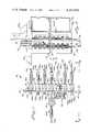
- FIG. 1is a fragmentary side elevational view of an electrical system including a plurality of fixed connectors holding circuit cards in congested relation on one side of a master interconnect board and illustrating an adapter according to the present invention for transferring the electrical connections of a circuit card of the system from a fixed connector in the congested area on one side of the master board to a convenient access area on the opposite side of the board;
- FIG. 2is a view taken about on lines 2--2 in FIG. 1 in the direction of the arrows;
- FIG. 3is a sectional view taken about on lines 3--3 in FIG. 2;
- FIG. 4is a fragmentary elevational view taken about on line 4--4 in FIG. 3.
- an adaptertransfers the electrical connections of a circuit card of an electrical system from a chassis connector or fixed connector in a congested chassis area on one side of the master interconnect board to a convenient access area on the opposite side of the board.
- the adaptercomprises first means for making electrical connection to the system at a location on the opposite side of the master board in correspondence with the fixed connector, second means for making electrical connection to the circuit card, and means defining an electrical path between the first and second means, the path having a length no greater than about triple the length of the electrical path through the fixed connector between the master board and the circuit card connected to the chassis connector.
- the adapterpreferably comprises a first electrical connector element for making electrical connection to the system at a location on the opposite side of the master board in correspondence with the fixed connector, a second electrical connector element for making electrical connection to the circuit card, and means for joining the first and second electrical connector elements mechanically and electrically adjacent the opposite side of the master board.
- the joining meanscomprises a rigid element having mechanical connection to the two electrical connector elements and having electrically conductive paths thereon for conveying signals between the two electrical connectors in a predetermined manner.
- an electrical assemblygenerally designated 10 includes a plurality of circuit boards or cards 12, in the present example seven circuit cards 12a-12g, arranged in a closely-stacked arrangement.
- the circuit cards 12are shown fragmentarily, the cards being rectangular in shape and of various sizes with a somewhat standardized thickness in the range of from about 0.054 inch to about 0.070 inch.
- the cards 12are disposed in substantially parallel, closely-spaced planes.
- Each of the cards or boards 12contains electrical components and conductors etched or printed thereon in a selected circuit configuration and in a known manner.
- the circuit cards 12are mechanically carried by a chassis including a reference board designated 14, also known as a master interconnector board, which serves as a frame.
- the reference board 14which is generally rectangular in shape, includes oppositely directed planar surfaces 16 and 18.
- One side of the reference board, in the assembly shown the side adjacent the surface 16,includes the plurality of circuit cards 12 and corresponding electrical connectors in closely-spaced relation thereby providing a rather congested area.
- the circuit cards 12 when connected electrically through connectors to the reference board 14comprise an operative part of the electrical system.
- the region adjacent the opposite surface 18 of reference board 14is relatively uncongested and provides an area of convenient access.
- the reference board 14is disposed generally vertically, the circuit boards 12 are disposed generally horizontally and extend outwardly from surface 16 of reference board 14 in a manner facing toward the front portion of the chassis.
- the surface 18 of board 14typically is in the rear region of the chassis.
- the circuit cards 12are connected to the reference board 14 by a corresponding plurality of chassis or fixed connectors 20.
- chassis or fixed connectors 20In the assembly shown there are seven connectors 20a-20g, one connector being provided for each of the circuit boards 12a-12g, respectively.
- Each electrical connector element 20is stationary during operation of the apparatus and serves to hold the corresponding circuit card thereby providing mechanical support for the same and simultaneously providing electrical connections between the card and other connectors or system connection points whereby each of the circuit cards 12 is electrically connected to the remainder of the system.
- each electrical connector element 20has an elongated body of rectangular shape which receives an edge of the corresponding circuit card 12 in a clamping-like or gripping manner. Electrical contacts in the connector body engage corresponding electrical contact portions or regions provided at spaced locations along the edge of the circuit card.
- the electrical contacts of the chassis or fixed connectorinclude portions which fit into the reference board 14, and in the arrangement shown those connector portions extend through the reference board to the other side in the form of wrap post elements designated 22 and 24 in FIG. 1, in particular 22a-22g and 24a-24g corresponding to each of the chassis connectors 20a-20g.
- the posts or pins of one connectorare connected electrically to the pins of another connector or to an appropriate system location. Alternatively, electrical connections could be made through board 14.
- the electrical connectors 20can be those commercially available from AMP incorporated known as zero insertion force printed circuit connectors and shown in AMP data sheet number 76-376 dated October 1976.
- the body of each connectoris of synthetic plastic material, for example glass-filled nylon, and the electrical contact elements within the connector body can be of copper.
- Each connector 20includes a lever or handle 30 which is pivotally connected to the housing 20 and mechanically connected to camming elements (not shown) within body 20 so that during movement between two positions the lever 30 moves components of the body between a position releasing the circuit card element and a position clamping or firmly gripping the element. As shown in FIG.
- lever 30gis set in a position causing connector body 20g to clamp or hold the circuit card 12g, and is movable to the position shown in broken lines wherein it allows the circuit board 12g to be removed from the body 20g.
- levers 30a-30gare associated with connectors 20a-20g respectively.
- each connector bodysuch as that of connector 20e includes a pair of opposed sidewall portions generally designated 34e-36e.
- the sidewall portions 34e, 36eare moved toward and away from each other in response to movement of lever or handle 30e between the two positions shown in FIG. 2.
- the connector 20eincludes a pair of electrical contact strip elements 38e,40e of copper or similar electrical conducting material which can be gold-plated at appropriate contact areas or portions thereon.
- the contact strip elements 38e,40einclude sections at one end defining the wrap posts 22e,24e shown in FIG. 1.
- the contact strips 38e and 40einclude intermediate portions 42e and 44e shown in FIG.
- the portions 42e and 44eare offset from the adjacent body portions of the strips 38e and 40e as shown in FIG. 3 in a manner facilitating a firm but releaseable contact between the inner surfaces of the apertures and the strip sections 42e,44e and adjacent strip body portions.
- the electrical contact strip elements 38e and 40eare formed to include intermediate leg or foot portions 50e and 52e respectively extending outwardly so as to engage or contact the inner wall surface of the corresponding side portion 34e and 36e, respectively.
- the foot portions 50e,52eserve to support and position the contact strip elements 38e,40e.
- the opposite ends of the strip elementsare formed to include contact portions 54e,56e adjacent the open end of the connector body 20e for making electrical contact with the circuit card 12e. In particular, when the circuit card 12e is inserted into the open end of the connector body, the contact portions 54e and 56e engage or contact electrically conductive regions 58e and 60e on opposite surfaces of the circuit card 12.
- the resiliency or spring of the contact strip elements 38e and 40e, the urging force of the foot members 50e and 52e and the force provided by the side wall portions 34e,36e being urged together by the lever and cam actionall provide an effective electrical contact between the portions 54 and 56 and the regions 58 and 60, respectively.
- the foregoingalso provides sufficient mechanical gripping force to hold the circuit card 12e in place.
- the lever 30eincludes a groove or recess along the one surface to receive the edge of the circuit card as shown in FIG. 2 thereby also supporting the card.
- both the received edge of the circuit card 12e and the connector body 20eare of considerable length in a direction perpendicular to the plane of the paper as viewed in FIG. 3.
- the circuit card 12eincludes a plurality of discrete contact regions 58e and 60e at spaced locations along the edge thereof.
- the connector body 20eis provided with a corresponding plurality of contact strip elements 38e and 40e at spaced locations along the length thereof.
- the large number of discrete contact regions 58e and 60e along the edge thereofmate with a corresponding plurality of electrical contact strip elements 38e and 40e.
- each circuit card 12a-12g and corresponding connector elements 20a-20git being understood that a plurality of circuit cards and chassis connector elements typically are connected to one side of the reference board 14 thereby providing a stacked arrangement of circuit cards and connectors in a relatively congested, closely-spaced arrangement.
- circuit cards and connectorsare positioned closely adjacent to enable a large number thereof to be included in a given chassis area which makes difficult and in most instances impossible any access to a particular circuit card and components thereon while the card is connected in the stacked assembly. This is especially so due to the fact that the circuit cards usually are of considerable length in a direction perpendicular to the plane of the reference board 14.
- an adapterfor transferring the electrical connections of a circuit card of an electrical system from a chassis or stationary connector in a congested chassis area or region on one side of the reference board to a convenient access area on the opposite side of the reference board.
- the adaptercomprises a first electrical connector element generally designated 66 for making electrical connection to the system at a location on the opposite side of the reference board 14 in correspondence with a particular chassis connector 20.
- the adapterfurther comprises a second electrical connector element generally designated 70 for making electrical connection to the circuit card 12, and means in the form of a circuit board element 72 for joining the first and second electrical connector elements mechanically and electrically adjacent the opposite side 18 of the reference board 14.
- a selected circuit card element 12can be disconnected from the corresponding chassis connector 20 and moved to the uncongested area or region adjacent the opposite side of the reference board 14 and connected to the second electrical connector element 70 of the adapter to facilitate working on the circuit card in a manner which does not increase significantly the electrical path length from the reference board 14 to the circuit card 12.
- Electrical connector 66includes an elongated rectangular shaped body having one side portion adapted to receive the wrap post elements 22,24 extending through the reference board 14 from the corresponding chassis connector 20.
- connector 66receives the wrap post elements 22e,24e extending through reference board 14 from chassis connector 20e.
- the connector element 66includes a handle or lever 74 as shown in FIG. 2 which cooperates with camming elements in the connector body whereby components thereof are moved between two positions to release and hold the wrap post elements.
- the body of connector 66 as shown in FIG. 3includes a pair of sidewall portions 78,80 and the connector also includes an intermediate wall portion 81 disposed between side wall portions 78,80 thereby defining two spaced regions there between.
- the sidewall portions 78,80are moved toward and away from the intermediate wall 81 in response to the movement of handle 74 in a manner similar to chassis connector 20.
- the connector 66further includes a pair of electrical contact strip elements 82 and 84 of suitable electrical conducting materials such as copper and gold-plated at appropriate locations similar to strips 38,40 of the chassis connector 20.
- the contact strip elements 82,84are located in the regions or chambers defined between the intermediate wall 81 and the corresponding side wall portion 78 and 80.
- the contact strip elements 82 and 84include sections 86 and 88, respectively, located in the region near the end of the body of connector 66 which receives the wrap post elements.
- the contact surface portions 86 and 88are adapted to engage or contact corresponding wrap post 22 and 24, respectively, which extend into the connector body into the regions between side walls 78,80 and intermediate wall 81.
- the contact strip elements 82 and 84are provided with leg or foot-like portions 90 and 92, respectively adjacent the opposite side of the connector body which engage inner surfaces of the corresponding side wall portions 78 and 80 for maintaining position of the contact strip elements.
- the contact strip elements 82 and 84extend outwardly from the body of connector 66 and are formed to include contact portions 94 and 96 adapted to fit in and make electrical contact with the inner surfaces of apertures provided with layers or coatings of electrically conductive material 98 and 100, respectively, such as metal.
- each contact strip element 82, 84 between the corresponding foot 90,92 and contact section 86,88is disposed angularly outwardly relative to intermediate wall 81 to enhance the gripping or contacting spring force between sections 86,88 and the corresponding wrap post elements.
- Such forceis provided by the resiliency or spring of the contact strip elements 82,84, the urging force of the foot members 90,92 and the force provided by the side wall portions 78,80 being urged together by the lever and cam action.
- Electrical connector 70is substantially similar to one of the chassis connectors 20 and includes a lever 104 shown in FIG. 1 which is pivotally connected to the connector housing and mechanically connected to camming elements (not shown) within the connector housing so that during movement between two positions the lever 104 moves components of the connector housing or body between a position clamping or firmly gripping a circuit card and a position releasing the card.
- lever 104is shown in a position causing the body of connector 70 to clamp or hold the circuit card 12e which has been removed from the opposite side of reference board 14. As shown in more detail in FIG.
- the body of connector 70includes a pair of opposed sidewall portions 108,110 moveable toward and away from each other in response to operation of lever 104 in a manner similar to that of chassis connector 20.
- a pair of contact strip elements 112 and 114are included in connector 70 similar to contact strip elements 38 and 40, respectively of the chassis connectors.
- the contact strip elements 112 and 114have end contact portions 116 and 118, respectively, feet or leg portions 120 and 122, respectively, and offset contact portions 124 and 126 respectively.
- the contact portions 124 and 126are received in apertures in circuit board 72 provided with coatings or regions 128 and 130 of electrical conducting material such as metal.
- the portions 124 and 126are offset from adjacent body portions of the strips 112 and 114, respectively, as shown in FIG.
- the contact strip elements 124 and 126terminate in end portions 132 and 134, respectively, which extend beyond board 72.
- the metal-plated conductive apertures 98 and 130 of the circuit board 72are connected electrically by a band or strip 138 of electrically conducting material, such as metal deposited or plated on the surface of board 72.
- Board 72includes a series of related apertures 98,130 arranged in a direction perpendicular to the plane of the paper as viewed in FIG. 3. This is shown in further detail in FIG. 4 which illustrates three sets of apertures 98,130, 98',130' and 98",130" and connecting paths 138,138', 138".
- a typical adapterwould include a large number of such sets.
- the metal plated conductive apertures 100 and 128are connected electrically by bands or strips 140 of electrically conducting material such as metal applied to the surface of board 72, in the device shown on the opposite surface of board 72. Alternatively, these strips could be on the same surface of board 72. As shown in FIG. 4 the sets of apertures 100,128 100',128' and 100",128" are connected electrically by paths 140,140' and 140", and a typical adapter would include a large number of such sets. In the foregoing arrangement, circuit board 72 would be of insulative material.
- circuit card 72has a minimum width of about 1.1 inch, the distance between the centers of plated apertures 100 and 128 measured perpendicular to the longitudinal axis of card 72 is about 0.6 inch, the distance between the center of apertures 98,100 is about 0.1 inch and the same distance exists between apertures 128, 130.
- the circuit card adapter of the present inventionoperates in the following manner when it is desired to perform work on one of the circuit cards in the closely-stacked arrangement,for example making tests on or repairs to circuit components or portions of an individual card.
- the circuit card of interestis selected, and the location on the opposite side of the chassis or reference board 14 in correspondence with this particular circuit card and its chassis connector is identified.
- the circuit card adaptercomprising connectors 66 and 70 joined by element 72 is connected to chassis board 14 at a location on the opposite side 18 thereof in correspondence with the chassis connector 20e.
- lever 30e of chassis connector 20eis manipulated to release circuit card 12e which is removed form the congested area of the closely stacked circuit cards 12s-12g on the outside of the reference board 14 and then transferred to the uncongested, open area adjacent the opposite side 18 of board 14.
- Lever 104is manipulated to move the side walls of connector 70 to an open position, and the edge of circuit card 12e bearing the contact portions is inserted into the open side of connector 70.
- circuit card 12e when received in connector 70is displaced 180° about an axis perpendicular to the plane of card 12e relative to the original sense or orientation when received in connector 20.
- Lever 104then is manipulated to a position wherein the side walls of connector 70 close on the edge of card 12e so that connector 70 makes electrical connection to the contact portions on the edge of the circuit card, as well as making mechanical connection to the card along the edge thereof.
- the contact portions 86 and 88 of the contact strip elements 82 and 84, respectively, of connector 66make electrical connection to the wrap post elements or terminals 22 and 24, respectively, which are connected electrically to post elements of other connectors or to appropriate system locations as previously described.
- the contact portions 116 and 118 of contact strip elements 112 and 114, respectively, of connector 70make electrical connection to the circuit card, in partiuclar to the conductive sections 60 and 58 along the edge thereof.
- An electrical pathis defined between contact portion 86 of connector 66 and contact portion 118 of connector 70 as follows: from contact portion 86 through contact strip element 82, through conductive plated aperture 98 on board 72, through conductive path 138, through conductive plated aperture 130, through contact strip element 114 of connector 70 to contact portion 118.
- An electrical pathis defined between contact portion 88 of connector 66 and contact portion 116 of connector 70 as follows: from contact portion 88 through contact strip element 84, through conductive path 140, through conductive plated aperture lining 128, through contact strip element 112 of connector 70 to contact portion 116.
- Each of the foregoing sets of pathsis provided by the connectors 66 and 70 and circuit card 72 of the adapter for each of the large number of positions described above corresponding to the sets of wrap post elements, for example in a typical range of 15-75 positions.
- each of the two electrical paths described above, the two paths defining one set,has substantially the same length.
- the length of each pathis significantly less than the distance measured along the circuit card 12 in an outward direction from the plane of reference board 14 as viewed in FIGS. 1 or 3 when the circuit card 12 is connected to its chassis connector 20.
- the length of the electrical signal path between circuit card 12 and reference board 14 through the adapter of the present inventionis considerably less than the electrical signal path through extender cards heretofore available.
- the length of the electrical signal path through the adapter of the present inventionincludes the width of connector element 66, the width of connector element 70 and the distance along the paths 130, 140 on board 72.
- the width of connector 70 and of connector 66is measured parallel to the plane of the paper as viewed in FIG. 3. In the apparatus shown, this electrical path length is substantially no greater than about three times the length of the electrical path through the corresponding chassis connector 20 between reference board 14 and the circuit card 12 when it is connected to the chassis connector.
- circuit card 12eWith the circuit card 12e mechanically held by the adapter adjacent side 18 of reference board 14 and extending outwardly from the plane of reference board 14,18 and with circuit card 12e electrically connected to the wrap posts of its connector 20 by the adapter, the electrical connections of circuit card 12e of the electrical system have been transferred by the adapter from the chassis connector 20 in a congested area on side 16 of reference board 14 to a convenient access area on the opposite side 18 of the reference board.
- the circuit 12behaves or functions electrically in the system in the same manner as it did when connected to its chassis connector. As shown in FIG.
- the card test adapterwhich includes the two connectors 66 and 70 joined mechanically and electrically by circuit board 72 is simple in construction, effective in operation and convenient to use. The nature of the connectors provides easy connection and disconnection of the circuit card and also the card test adapter as well.
- lever 104When the operations such as testing and repair have been completed on circuit card 12e, lever 104 is moved to a position releasing the circuit card from connector 70 whereupon the card is returned and reconnected to its chassis connector 20e.
- the adaptercan be removed from reference board 14 for re-connection to another location on side 18 of the board in correspondence with the chassis connector of another circuit card on which it is desired to perform trouble shooting or other work in the uncongested area adjacent side 18 of the reference board.
Landscapes
- Coupling Device And Connection With Printed Circuit (AREA)
Abstract
Description
Claims (21)
Priority Applications (1)
| Application Number | Priority Date | Filing Date | Title |
|---|---|---|---|
| US05/953,645US4232924A (en) | 1978-10-23 | 1978-10-23 | Circuit card adapter |
Applications Claiming Priority (1)
| Application Number | Priority Date | Filing Date | Title |
|---|---|---|---|
| US05/953,645US4232924A (en) | 1978-10-23 | 1978-10-23 | Circuit card adapter |
Publications (1)
| Publication Number | Publication Date |
|---|---|
| US4232924Atrue US4232924A (en) | 1980-11-11 |
Family
ID=25494313
Family Applications (1)
| Application Number | Title | Priority Date | Filing Date |
|---|---|---|---|
| US05/953,645Expired - LifetimeUS4232924A (en) | 1978-10-23 | 1978-10-23 | Circuit card adapter |
Country Status (1)
| Country | Link |
|---|---|
| US (1) | US4232924A (en) |
Cited By (50)
| Publication number | Priority date | Publication date | Assignee | Title |
|---|---|---|---|---|
| WO1982001621A1 (en)* | 1980-10-24 | 1982-05-13 | Computer Corp Nanodata | Circuit card adapter |
| US4352533A (en)* | 1978-10-31 | 1982-10-05 | Fujitsu Limited | Connector device for printed boards |
| US4692120A (en)* | 1986-10-01 | 1987-09-08 | Feinstein David Y | Electronic card for sharing the same edgeboard connector with another electronic edgeboard |
| US4907977A (en)* | 1988-10-14 | 1990-03-13 | Ncr Corporation | Computer backpanel inversion coupler |
| US5006080A (en)* | 1989-06-21 | 1991-04-09 | Hosiden Electronics Co., Ltd. | Electrical connector |
| US5059130A (en)* | 1988-06-23 | 1991-10-22 | Ltv Aerospace And Defense Company | Minimal space printed cicuit board and electrical connector system |
| WO1993015534A1 (en)* | 1992-01-22 | 1993-08-05 | Connector Systems Technology N.V. | A system and connectors for the electrical interconnection of component boards |
| US5335146A (en)* | 1992-01-29 | 1994-08-02 | International Business Machines Corporation | High density packaging for device requiring large numbers of unique signals utilizing orthogonal plugging and zero insertion force connetors |
| US5488541A (en)* | 1994-05-31 | 1996-01-30 | Northern Telecom Limited | VME bus compatible backplane and shelf arrangement |
| EP0685907A3 (en)* | 1994-05-30 | 1997-01-29 | Whitaker Corp | Contact and connector. |
| US5800186A (en)* | 1997-03-13 | 1998-09-01 | Framatome Connectors Usa, Inc. | Printed circuit board assembly |
| US6129575A (en)* | 1998-12-21 | 2000-10-10 | Lucent Technologies Inc. | Testing system for a connector with a self-sealing connector housing |
| US6129577A (en)* | 1998-12-21 | 2000-10-10 | Lucent Technologies Inc. | Connector testing system having connector latching |
| US6280236B1 (en) | 1998-12-21 | 2001-08-28 | Avaya Technology Corp. | Testing system with bridge clip, and connector having a positive stop |
| US6302725B1 (en) | 1998-12-21 | 2001-10-16 | Avaya Technology Corporation | Self-latching terminal strip |
| US6340306B1 (en) | 1998-12-21 | 2002-01-22 | Avaya Technology Corp. | Bridge clip for a connector |
| US6373259B1 (en) | 1999-03-09 | 2002-04-16 | Avaya Technology Corp. | Connector testing system having a test prong including a projection |
| US20030007339A1 (en)* | 2001-07-05 | 2003-01-09 | Harris Mark Roy | Stacked backplane assembly |
| US20040010638A1 (en)* | 1994-03-11 | 2004-01-15 | Silicon Bandwidth, Inc. | Modular architecture for high bandwidth computers |
| US20050186810A1 (en)* | 2003-06-27 | 2005-08-25 | Emc Corporation | Invertible, pluggable module for variable I/O densities |
| WO2006110526A3 (en)* | 2005-04-07 | 2007-09-20 | Fci Americas Technology Inc | Orthogonal backplane connector |
| US20070287336A1 (en)* | 2006-06-09 | 2007-12-13 | Buck Jonathan E | Electrical connectors with alignment guides |
| US20080207011A1 (en)* | 2005-01-11 | 2008-08-28 | Fci | Board-To-Board Connector |
| US7497736B2 (en) | 2006-12-19 | 2009-03-03 | Fci Americas Technology, Inc. | Shieldless, high-speed, low-cross-talk electrical connector |
| US7497735B2 (en) | 2004-09-29 | 2009-03-03 | Fci Americas Technology, Inc. | High speed connectors that minimize signal skew and crosstalk |
| US7500871B2 (en) | 2006-08-21 | 2009-03-10 | Fci Americas Technology, Inc. | Electrical connector system with jogged contact tails |
| US20090067146A1 (en)* | 2007-09-06 | 2009-03-12 | International Business Machines Corporation | Electronic Board Arrangement and Electronic Interconnect Board of an Electronic Board Arrangement |
| US20090130912A1 (en)* | 2007-11-15 | 2009-05-21 | Fci Americas Technology, Inc. | Electrical connector mating guide |
| US20100055988A1 (en)* | 2007-08-30 | 2010-03-04 | Shuey Joseph B | Mezzanine-type electrical connectors |
| US20100075516A1 (en)* | 2008-09-25 | 2010-03-25 | Horchler David C | Hermaphroditic Electrical Connector |
| US20100167569A1 (en)* | 2008-12-31 | 2010-07-01 | Stoner Stuart C | Gender-Neutral Electrical Connector |
| US7967647B2 (en)* | 2007-02-28 | 2011-06-28 | Fci Americas Technology Llc | Orthogonal header |
| US8137119B2 (en) | 2007-07-13 | 2012-03-20 | Fci Americas Technology Llc | Electrical connector system having a continuous ground at the mating interface thereof |
| US8267721B2 (en) | 2009-10-28 | 2012-09-18 | Fci Americas Technology Llc | Electrical connector having ground plates and ground coupling bar |
| US8540525B2 (en) | 2008-12-12 | 2013-09-24 | Molex Incorporated | Resonance modifying connector |
| US8545240B2 (en) | 2008-11-14 | 2013-10-01 | Molex Incorporated | Connector with terminals forming differential pairs |
| US8616919B2 (en) | 2009-11-13 | 2013-12-31 | Fci Americas Technology Llc | Attachment system for electrical connector |
| US8764464B2 (en) | 2008-02-29 | 2014-07-01 | Fci Americas Technology Llc | Cross talk reduction for high speed electrical connectors |
| USD718253S1 (en) | 2012-04-13 | 2014-11-25 | Fci Americas Technology Llc | Electrical cable connector |
| US8905651B2 (en) | 2012-01-31 | 2014-12-09 | Fci | Dismountable optical coupling device |
| USD720698S1 (en) | 2013-03-15 | 2015-01-06 | Fci Americas Technology Llc | Electrical cable connector |
| US8944831B2 (en) | 2012-04-13 | 2015-02-03 | Fci Americas Technology Llc | Electrical connector having ribbed ground plate with engagement members |
| USD727268S1 (en) | 2012-04-13 | 2015-04-21 | Fci Americas Technology Llc | Vertical electrical connector |
| USD727852S1 (en) | 2012-04-13 | 2015-04-28 | Fci Americas Technology Llc | Ground shield for a right angle electrical connector |
| US9048583B2 (en) | 2009-03-19 | 2015-06-02 | Fci Americas Technology Llc | Electrical connector having ribbed ground plate |
| USD733662S1 (en) | 2013-01-25 | 2015-07-07 | Fci Americas Technology Llc | Connector housing for electrical connector |
| USD746236S1 (en) | 2012-07-11 | 2015-12-29 | Fci Americas Technology Llc | Electrical connector housing |
| US9257778B2 (en) | 2012-04-13 | 2016-02-09 | Fci Americas Technology | High speed electrical connector |
| US9277649B2 (en) | 2009-02-26 | 2016-03-01 | Fci Americas Technology Llc | Cross talk reduction for high-speed electrical connectors |
| US9543703B2 (en) | 2012-07-11 | 2017-01-10 | Fci Americas Technology Llc | Electrical connector with reduced stack height |
Citations (4)
| Publication number | Priority date | Publication date | Assignee | Title |
|---|---|---|---|---|
| US3663925A (en)* | 1970-05-20 | 1972-05-16 | Us Navy | Electrical connector |
| GB1313641A (en)* | 1971-09-28 | 1973-04-18 | Ncr Co | Electrical connector for printed circuit cards |
| US3930707A (en)* | 1974-06-10 | 1976-01-06 | A P Products Incorporated | Interface connector |
| US4080028A (en)* | 1976-12-09 | 1978-03-21 | Powell Electrical Manufacturing Company | Printed circuit board connector adapter |
- 1978
- 1978-10-23USUS05/953,645patent/US4232924A/ennot_activeExpired - Lifetime
Patent Citations (4)
| Publication number | Priority date | Publication date | Assignee | Title |
|---|---|---|---|---|
| US3663925A (en)* | 1970-05-20 | 1972-05-16 | Us Navy | Electrical connector |
| GB1313641A (en)* | 1971-09-28 | 1973-04-18 | Ncr Co | Electrical connector for printed circuit cards |
| US3930707A (en)* | 1974-06-10 | 1976-01-06 | A P Products Incorporated | Interface connector |
| US4080028A (en)* | 1976-12-09 | 1978-03-21 | Powell Electrical Manufacturing Company | Printed circuit board connector adapter |
Cited By (86)
| Publication number | Priority date | Publication date | Assignee | Title |
|---|---|---|---|---|
| US4352533A (en)* | 1978-10-31 | 1982-10-05 | Fujitsu Limited | Connector device for printed boards |
| WO1982001621A1 (en)* | 1980-10-24 | 1982-05-13 | Computer Corp Nanodata | Circuit card adapter |
| US4692120A (en)* | 1986-10-01 | 1987-09-08 | Feinstein David Y | Electronic card for sharing the same edgeboard connector with another electronic edgeboard |
| US5059130A (en)* | 1988-06-23 | 1991-10-22 | Ltv Aerospace And Defense Company | Minimal space printed cicuit board and electrical connector system |
| US4907977A (en)* | 1988-10-14 | 1990-03-13 | Ncr Corporation | Computer backpanel inversion coupler |
| US5006080A (en)* | 1989-06-21 | 1991-04-09 | Hosiden Electronics Co., Ltd. | Electrical connector |
| US5707242A (en)* | 1992-01-22 | 1998-01-13 | Mitra; Niranjan Kumar | System and connectors for the electrical interconnection of component boards |
| WO1993015534A1 (en)* | 1992-01-22 | 1993-08-05 | Connector Systems Technology N.V. | A system and connectors for the electrical interconnection of component boards |
| US5335146A (en)* | 1992-01-29 | 1994-08-02 | International Business Machines Corporation | High density packaging for device requiring large numbers of unique signals utilizing orthogonal plugging and zero insertion force connetors |
| US7803020B2 (en) | 1994-03-11 | 2010-09-28 | Crane Jr Stanford W | Backplane system having high-density electrical connectors |
| US20080005442A1 (en)* | 1994-03-11 | 2008-01-03 | The Panda Project | Backplane system having high-density electrical connectors |
| US7103753B2 (en) | 1994-03-11 | 2006-09-05 | Silicon Bandwith Inc. | Backplane system having high-density electrical connectors |
| US20100323536A1 (en)* | 1994-03-11 | 2010-12-23 | Wolpass Capital Inv., L.L.C. | Backplane system having high-density electrical connectors |
| US20040010638A1 (en)* | 1994-03-11 | 2004-01-15 | Silicon Bandwidth, Inc. | Modular architecture for high bandwidth computers |
| EP0685907A3 (en)* | 1994-05-30 | 1997-01-29 | Whitaker Corp | Contact and connector. |
| US5488541A (en)* | 1994-05-31 | 1996-01-30 | Northern Telecom Limited | VME bus compatible backplane and shelf arrangement |
| US5800186A (en)* | 1997-03-13 | 1998-09-01 | Framatome Connectors Usa, Inc. | Printed circuit board assembly |
| US6340306B1 (en) | 1998-12-21 | 2002-01-22 | Avaya Technology Corp. | Bridge clip for a connector |
| US6302725B1 (en) | 1998-12-21 | 2001-10-16 | Avaya Technology Corporation | Self-latching terminal strip |
| US6280236B1 (en) | 1998-12-21 | 2001-08-28 | Avaya Technology Corp. | Testing system with bridge clip, and connector having a positive stop |
| US6129577A (en)* | 1998-12-21 | 2000-10-10 | Lucent Technologies Inc. | Connector testing system having connector latching |
| US6129575A (en)* | 1998-12-21 | 2000-10-10 | Lucent Technologies Inc. | Testing system for a connector with a self-sealing connector housing |
| US6373259B1 (en) | 1999-03-09 | 2002-04-16 | Avaya Technology Corp. | Connector testing system having a test prong including a projection |
| US6757177B2 (en)* | 2001-07-05 | 2004-06-29 | Tropic Networks Inc. | Stacked backplane assembly |
| US20030007339A1 (en)* | 2001-07-05 | 2003-01-09 | Harris Mark Roy | Stacked backplane assembly |
| US20050186810A1 (en)* | 2003-06-27 | 2005-08-25 | Emc Corporation | Invertible, pluggable module for variable I/O densities |
| US7290330B2 (en)* | 2003-06-27 | 2007-11-06 | Emc Corporation | Coupling invertible and pluggable module to a circuit board |
| US7497735B2 (en) | 2004-09-29 | 2009-03-03 | Fci Americas Technology, Inc. | High speed connectors that minimize signal skew and crosstalk |
| US20080207011A1 (en)* | 2005-01-11 | 2008-08-28 | Fci | Board-To-Board Connector |
| US7905729B2 (en)* | 2005-01-11 | 2011-03-15 | Fci | Board-to-board connector |
| WO2006110526A3 (en)* | 2005-04-07 | 2007-09-20 | Fci Americas Technology Inc | Orthogonal backplane connector |
| US20070287336A1 (en)* | 2006-06-09 | 2007-12-13 | Buck Jonathan E | Electrical connectors with alignment guides |
| US7553182B2 (en)* | 2006-06-09 | 2009-06-30 | Fci Americas Technology, Inc. | Electrical connectors with alignment guides |
| US7500871B2 (en) | 2006-08-21 | 2009-03-10 | Fci Americas Technology, Inc. | Electrical connector system with jogged contact tails |
| US7837505B2 (en) | 2006-08-21 | 2010-11-23 | Fci Americas Technology Llc | Electrical connector system with jogged contact tails |
| US7497736B2 (en) | 2006-12-19 | 2009-03-03 | Fci Americas Technology, Inc. | Shieldless, high-speed, low-cross-talk electrical connector |
| US8096832B2 (en) | 2006-12-19 | 2012-01-17 | Fci Americas Technology Llc | Shieldless, high-speed, low-cross-talk electrical connector |
| US7762843B2 (en) | 2006-12-19 | 2010-07-27 | Fci Americas Technology, Inc. | Shieldless, high-speed, low-cross-talk electrical connector |
| US8382521B2 (en) | 2006-12-19 | 2013-02-26 | Fci Americas Technology Llc | Shieldless, high-speed, low-cross-talk electrical connector |
| US8678860B2 (en) | 2006-12-19 | 2014-03-25 | Fci Americas Technology Llc | Shieldless, high-speed, low-cross-talk electrical connector |
| US7967647B2 (en)* | 2007-02-28 | 2011-06-28 | Fci Americas Technology Llc | Orthogonal header |
| US8057267B2 (en) | 2007-02-28 | 2011-11-15 | Fci Americas Technology Llc | Orthogonal header |
| US8137119B2 (en) | 2007-07-13 | 2012-03-20 | Fci Americas Technology Llc | Electrical connector system having a continuous ground at the mating interface thereof |
| US20100055988A1 (en)* | 2007-08-30 | 2010-03-04 | Shuey Joseph B | Mezzanine-type electrical connectors |
| US8147268B2 (en) | 2007-08-30 | 2012-04-03 | Fci Americas Technology Llc | Mezzanine-type electrical connectors |
| US20090067146A1 (en)* | 2007-09-06 | 2009-03-12 | International Business Machines Corporation | Electronic Board Arrangement and Electronic Interconnect Board of an Electronic Board Arrangement |
| US8358511B2 (en)* | 2007-09-06 | 2013-01-22 | International Business Machines Corporation | Electronic board arrangement and electronic interconnect board of an electronic board arrangement |
| US8147254B2 (en) | 2007-11-15 | 2012-04-03 | Fci Americas Technology Llc | Electrical connector mating guide |
| US20090130912A1 (en)* | 2007-11-15 | 2009-05-21 | Fci Americas Technology, Inc. | Electrical connector mating guide |
| US8764464B2 (en) | 2008-02-29 | 2014-07-01 | Fci Americas Technology Llc | Cross talk reduction for high speed electrical connectors |
| US20100075516A1 (en)* | 2008-09-25 | 2010-03-25 | Horchler David C | Hermaphroditic Electrical Connector |
| US8277241B2 (en) | 2008-09-25 | 2012-10-02 | Fci Americas Technology Llc | Hermaphroditic electrical connector |
| US8545240B2 (en) | 2008-11-14 | 2013-10-01 | Molex Incorporated | Connector with terminals forming differential pairs |
| US8992237B2 (en) | 2008-12-12 | 2015-03-31 | Molex Incorporated | Resonance modifying connector |
| US8651881B2 (en) | 2008-12-12 | 2014-02-18 | Molex Incorporated | Resonance modifying connector |
| US8540525B2 (en) | 2008-12-12 | 2013-09-24 | Molex Incorporated | Resonance modifying connector |
| US7976326B2 (en) | 2008-12-31 | 2011-07-12 | Fci Americas Technology Llc | Gender-neutral electrical connector |
| US20100167569A1 (en)* | 2008-12-31 | 2010-07-01 | Stoner Stuart C | Gender-Neutral Electrical Connector |
| US9277649B2 (en) | 2009-02-26 | 2016-03-01 | Fci Americas Technology Llc | Cross talk reduction for high-speed electrical connectors |
| US9048583B2 (en) | 2009-03-19 | 2015-06-02 | Fci Americas Technology Llc | Electrical connector having ribbed ground plate |
| US10720721B2 (en) | 2009-03-19 | 2020-07-21 | Fci Usa Llc | Electrical connector having ribbed ground plate |
| US10096921B2 (en) | 2009-03-19 | 2018-10-09 | Fci Usa Llc | Electrical connector having ribbed ground plate |
| US9461410B2 (en) | 2009-03-19 | 2016-10-04 | Fci Americas Technology Llc | Electrical connector having ribbed ground plate |
| US8267721B2 (en) | 2009-10-28 | 2012-09-18 | Fci Americas Technology Llc | Electrical connector having ground plates and ground coupling bar |
| US8616919B2 (en) | 2009-11-13 | 2013-12-31 | Fci Americas Technology Llc | Attachment system for electrical connector |
| US8905651B2 (en) | 2012-01-31 | 2014-12-09 | Fci | Dismountable optical coupling device |
| USD748063S1 (en) | 2012-04-13 | 2016-01-26 | Fci Americas Technology Llc | Electrical ground shield |
| US8944831B2 (en) | 2012-04-13 | 2015-02-03 | Fci Americas Technology Llc | Electrical connector having ribbed ground plate with engagement members |
| USD718253S1 (en) | 2012-04-13 | 2014-11-25 | Fci Americas Technology Llc | Electrical cable connector |
| USD816044S1 (en) | 2012-04-13 | 2018-04-24 | Fci Americas Technology Llc | Electrical cable connector |
| USD727852S1 (en) | 2012-04-13 | 2015-04-28 | Fci Americas Technology Llc | Ground shield for a right angle electrical connector |
| US9257778B2 (en) | 2012-04-13 | 2016-02-09 | Fci Americas Technology | High speed electrical connector |
| USD750030S1 (en) | 2012-04-13 | 2016-02-23 | Fci Americas Technology Llc | Electrical cable connector |
| USD750025S1 (en) | 2012-04-13 | 2016-02-23 | Fci Americas Technology Llc | Vertical electrical connector |
| USD727268S1 (en) | 2012-04-13 | 2015-04-21 | Fci Americas Technology Llc | Vertical electrical connector |
| US9831605B2 (en) | 2012-04-13 | 2017-11-28 | Fci Americas Technology Llc | High speed electrical connector |
| USD790471S1 (en) | 2012-04-13 | 2017-06-27 | Fci Americas Technology Llc | Vertical electrical connector |
| USD751507S1 (en) | 2012-07-11 | 2016-03-15 | Fci Americas Technology Llc | Electrical connector |
| US9543703B2 (en) | 2012-07-11 | 2017-01-10 | Fci Americas Technology Llc | Electrical connector with reduced stack height |
| US9871323B2 (en) | 2012-07-11 | 2018-01-16 | Fci Americas Technology Llc | Electrical connector with reduced stack height |
| USD746236S1 (en) | 2012-07-11 | 2015-12-29 | Fci Americas Technology Llc | Electrical connector housing |
| USD772168S1 (en) | 2013-01-25 | 2016-11-22 | Fci Americas Technology Llc | Connector housing for electrical connector |
| USD766832S1 (en) | 2013-01-25 | 2016-09-20 | Fci Americas Technology Llc | Electrical connector |
| USD733662S1 (en) | 2013-01-25 | 2015-07-07 | Fci Americas Technology Llc | Connector housing for electrical connector |
| USD745852S1 (en) | 2013-01-25 | 2015-12-22 | Fci Americas Technology Llc | Electrical connector |
| USD720698S1 (en) | 2013-03-15 | 2015-01-06 | Fci Americas Technology Llc | Electrical cable connector |
Similar Documents
| Publication | Publication Date | Title |
|---|---|---|
| US4232924A (en) | Circuit card adapter | |
| US6471541B2 (en) | Electrical connector for flat cables | |
| US4072387A (en) | Multiple conductor connector unit and cable assembly | |
| US4587596A (en) | High density mother/daughter circuit board connector | |
| US4017770A (en) | Connecting device for telecommunication circuits | |
| US4090667A (en) | Universally programmable shorting plug for an integrated circuit socket | |
| US3715706A (en) | Right angle electrical connector | |
| US6261132B1 (en) | Header connector for future bus | |
| EP0269248B1 (en) | Connector for flat flexible circuit members | |
| US6206713B1 (en) | PCB zero-insertion-force connector | |
| US4877409A (en) | Hinged electrical connector | |
| US4327955A (en) | Reduced insertion force connector | |
| US4270826A (en) | Zero insertion force connector | |
| US6386905B1 (en) | Flat cable connector | |
| US3930706A (en) | Circuit panel connector | |
| GB1184755A (en) | Improvements in or relating to Connector Assemblies for Printed Circuits | |
| JPH0719633B2 (en) | Electrical connector device | |
| CA1093174A (en) | Feed-through terminal block | |
| JPS5925343B2 (en) | Device for connecting electrical conductors in the form of conductors or wires to contact mechanisms | |
| US4512621A (en) | Flat cable pitch transition connector | |
| US3701078A (en) | Bussing connector | |
| WO1982001621A1 (en) | Circuit card adapter | |
| US6244878B1 (en) | Input/output connector with a connector body and terminals for a mobile electric device | |
| US4594490A (en) | Terminal pin shorting switch apparatus | |
| JP2537892Y2 (en) | IC test equipment |
Legal Events
| Date | Code | Title | Description |
|---|---|---|---|
| AS | Assignment | Owner name:CHEMICAL BANK 11 WEST 51ST., STREET, NY, NY 10019 Free format text:SECURITY INTEREST;ASSIGNOR:NANODATA COMPUTER CORPORATION A DE CORP;REEL/FRAME:004388/0238 Effective date:19850228 | |
| AS | Assignment | Owner name:CHEMICAL BANK, 11 WEST 51ST STREET, NEW YORK, NY 1 Free format text:SECURITY INTEREST;ASSIGNOR:NANODATA COMPUTER CORPORATION;REEL/FRAME:004417/0890 Effective date:19850228 Owner name:CHEMICAL BANK,NEW YORK Free format text:SECURITY INTEREST;ASSIGNOR:NANODATA COMPUTER CORPORATION;REEL/FRAME:004417/0890 Effective date:19850228 | |
| AS | Assignment | Owner name:INTELLITEK COMPUTER CORPORATION, NEBRASKA Free format text:CHANGE OF NAME;ASSIGNOR:FDR MERGER CORP.;REEL/FRAME:007205/0238 Effective date:19881128 Owner name:INTELLITEK COMPUTER CORPORATION, NEBRASKA Free format text:CHANGE OF NAME;ASSIGNOR:NANODATA COMPUTER CORPORATION;REEL/FRAME:007188/0977 Effective date:19850603 Owner name:INTELLITEK COMPUTER CORPORATION, NEBRASKA Free format text:CHANGE OF NAME;ASSIGNOR:FDR MERGER CORP.;REEL/FRAME:007205/0245 Effective date:19881128 | |
| AS | Assignment | Owner name:CABLE SERVICES GROUP, INC. A CORPORATION OF DEL Free format text:ASSIGNMENT OF ASSIGNORS INTEREST;ASSIGNOR:INTELLITEK COMPUTER CORPORATION;REEL/FRAME:007203/0550 Effective date:19941121 | |
| AS | Assignment | Owner name:BANQUE PARIBAS, CALIFORNIA Free format text:SECURITY INTEREST;ASSIGNOR:CABLE SERVICES GROUP, INC.;REEL/FRAME:007235/0359 Effective date:19941130 | |
| AS | Assignment | Owner name:INTELLITEK COMPUTER CORPORATION, NEBRASKA Free format text:RELEASE BY SECURED PARTY;ASSIGNOR:CHEMICAL BANK;REEL/FRAME:007235/0091 Effective date:19881228 Owner name:NANODATA COMPUTER CORPORATION, NEW YORK Free format text:RELEASE BY SECURED PARTY;ASSIGNOR:CHEMICAL BANK;REEL/FRAME:007235/0086 Effective date:19881228 |